

Page 1
High-performance Clock Generator Series
Compact 1ch Clock Generators
for Digital Cameras
BU3071HFV,BU3072HFV,BU3073HFV,BU3076HFV,BU7322HFV,BU7325HFV
●Description
These Clock Generators incorporates compact package compared to oscillators, which provides the generation of
high-frequency CCD, USB, VIDEO clocks necessary for digital still cameras and digital video cameras.
●Features
1) SEL pin allowing for the selection of frequencies
2) Selection of OE pin enabling Power-down function
3) Crystal-oscillator-level clock precision with high C/N characteristics and low jitter
4) Micro miniature HVSOF6 Package incorporated
5) Single power supply of 3.3 V
●Applications
Digital Still Camera, Digital Video Camera, and others
●Lineup
Parameter BU3071HFV BU3072HFV BU3073HFV BU3076HFV BU7322HFV BU7325HFV
Supply voltage 3.0 V ~ 3.6V 3.0 V ~ 3.6V 3.0 V ~ 3.6V 2.85 V ~ 3.6V 2.85 V ~ 3.6V 2.85 V ~ 3.6V
Operating temperature range -5℃ ~ 70℃ -5℃ ~ 70℃ -5℃ ~ 70℃ -5℃ ~ 75℃ -5℃ ~ 75℃ -30℃ ~ 85℃
Reference input clock 28.6363MHz 48.0000MHz 48.0000MHz 27.0000MHz 27.0000MHz 27.0000MHz
Output clock
Power-down function Provided Provided Provided Provided Provided Provided
Operating current (Typ.) 10mA 11mA 11mA 12mA 10mA 12mA
Package HVSOF6 HVSOF6 HVSOF6 HVSOF6 HVSOF6 HVSOF6
●Absolute Maximum Ratings(Ta=25℃)
Parameter Symbol Ratings Unit
Supply voltage VDD -0.3 ~ 4.0 V
Input voltage VIN -0.3 ~ VDD+0.3 V
Storage temperature range Tstg -30 ~ 125 ℃
Power dissipation Pd 410 mW
*1 Operating is not guaranteed.
*2 In the case of exceeding Ta = 25℃, 4.1mW should be reduced per 1℃.
*3 The radiation-resistance design is not carried out.
*4 Power dissipation is measured when the IC is mounted to the printed circuit board.
●Recommended Operating Range
Parameter Symbol Limits Unit
Supply voltage VDD 3.0 ~ 3.6 V
Input H voltage VINH 0.8VDD ~ VDD V
Input L voltage VINL 0.0 ~ 0.2VDD V
Operating temperature Topr -5 ~ 70 ℃
Output load CL 15(MAX) pF
54.0000MHz 27.0000MHz 24.3750MHz 54.0000MHz 49.5000MHz 48.0000MHz
- 36.0000MHz 24.5454MHz 67.5000MHz 36.0000MHz 78.0000MHz
No.09005EAT01
www.rohm.com
© 2009 ROHM Co., Ltd. All rights reserved.
1/21
2009.04 - Rev.A
Page 2

BU3071HFV,BU3072HFV,BU3073HFV,BU3076HFV,BU7322HFV,BU7325HFV
Technical Note
●Electrical Characteristics
BU3071HFV(Ta=25℃, VDD=3.3V,Crystal frequency=28.6363MHz, unless otherwise specified.)
Parameter Symbol
Min. Typ. Max.
Limits
Unit Conditions
Output H voltage VOH 2.8 - - V IOH=-4.0mA
Output L voltage VOL - - 0.5 V IOL=4.0mA
Consumption current 1 IDD1 - 10 15 mA OE=H, at no load
Consumption current 2 IDD2 - 1 1.3 mA OE=L
Output frequency - 54.0000 - MHz IN*264/35/4
The following parameters represent design guaranteed performance.
Duty Duty 45 50 55 % Measured at a voltage of 1/2 of VDD
Period-Jitter 1σ PJsSD - 50 - psec ※1
Period-Jitter MIN-MAX PJsABS - 300 - psec ※2
Period of transition time required for the
Rise time tr - 2.5 - nsec
output to reach 80% from 20% of VDD.
Provided with 15pF output load.
Period of transition time required for the
Fall time tf - 2.5 - nsec
output to reach 20% from 80% of VDD.
Provided with 15pF output load.
Output Lock time tLOCK - - 1 msec ※3
Note) The output frequency is determined by the arithmetic (frequency division) expression of a frequency input to IN.
If the input frequency is set to 28.6363MHz, the output frequency will be as listed above.
BU3072HFV(Ta=25℃, VDD=3.3V, Crystal frequency=48.0000MHz, unless otherwise specified.)
Parameter Symbol
Min. Typ. Max.
Limits
Unit Conditions
Output H voltage VOH 2.8 - - V IOH=-4.0mA
Output L voltage VOL - - 0.5 V IOL=4.0mA
Consumption current 1 IDD1 - 11 16 mA PD=H, at no load
Consumption current 2 IDD2 - - 5 µA PD=L
Output frequency
CLK_27 - 27.0000 - MHz SEL=L, IN*18/8/4
CLK_36 - 36.0000 - MHz SEL=H, IN*24/8/4
The following parameters represent design guaranteed performance.
Duty Duty 45 50 55 % Measured at a voltage of 1/2 of VDD
Period-Jitter 1σ PJsSD - 35 - psec ※1
Long-Term-Jitter
MIN-MAX
LTJsABS - 0.9 1.5 nsec
MIN-MAX of long-term jitter
(100 µsec from trigger)
Period of transition time required for the
Rise time tr - 2.5 - nsec
output to reach 80% from 20% of VDD.
Provided with 15pF output load.
Period of transition time required for the
Fall time tf - 2.5 - nsec
output to reach 20% from 80% of VDD.
Provided with 15pF output load.
Output Lock time tLOCK - - 1 msec ※3
Note) The output frequency is determined by the arithmetic (frequency division) expression of a frequency input to IN.
If the input frequency is set to 48.0000MHz, the output frequency will be as listed above.
www.rohm.com
© 2009 ROHM Co., Ltd. All rights reserved.
2/21
2009.04 - Rev.A
Page 3
BU3071HFV,BU3072HFV,BU3073HFV,BU3076HFV,BU7322HFV,BU7325HFV
Technical Note
BU3073HFV(Ta=25℃, VDD=3.3V, Crystal frequency=48.0000MHz, unless otherwise specified.)
Parameter Symbol
Min. Typ. Max.
Limits
Unit Conditions
Output H voltage VOH 2.8 - - V IOH=-4.0mA
Output L voltage VOL - - 0.5 V IOL=4.0mA
Consumption current 1 IDD1 - 11 16 mA PD=H, at no load
Consumption current 2 IDD2 - - 5 mA PD=L
Output frequency
CLK_375 - 24.3750 - MHz SEL=L, IN*65/16/8
CLK_545 - 24.5454 - MHz SEL=H, IN*45/11/8
The following parameters represent design guaranteed performance.
Duty Duty 45 50 55 % Measured at a voltage of 1/2 of VDD
Period-Jitter 1σ PJsSD - 45 - psec ※1
Long-Term-Jitter
MIN-MAX
LTJsABS - 0.9 1.5 nsec
MIN-MAX of long-term jitter
(100 µsec from trigger)
Period of transition time required for the
Rise time tr - 2.5 - nsec
output to reach 80% from 20% of VDD.
Provided with 15pF output load.
Period of transition time required for the
Fall time tf - 2.5 - nsec
output to reach 20% from 80% of VDD.
Provided with 15pF output load.
Output Lock time tLOCK - - 1 msec ※3
Note) The output frequency is determined by the arithmetic (frequency division) expression of a frequency input to IN.
If the input frequency is set to 48.0000MHz, the output frequency will be as listed above.
BU3076HFV(Ta=25℃, VDD=3.3V, Crystal frequency=27.0000MHz, unless otherwise specified.)
Parameter Symbol
Min. Typ. Max.
Limits
Unit Conditions
Output H voltage VOH 2.8 - - V IOH=-4.0mA
Output L voltage VOL - - 0.5 V IOL=4.0mA
Pull-down resistance Rpd 25 50 100 KΩ Pull-down resistance on input pin
Consumption current 1 IDD1 - 10 15 mA 54MHz output, at no load
Consumption current 2 IDD2 - 12 18 mA 67.5MHz output, at no load
Standby current IDDst - - 1 µA OE=L
Output frequency
CLK_54 - 54.0000 - MHz SEL=L, IN*48/6/4
CLK_67.5 - 67.5000 - MHz SEL=H, IN*60/6/4
The following parameters represent design guaranteed performance.
Duty Duty 45 50 55 % Measured at a voltage of 1/2 of VDD
Period-Jitter 1σ PJsSD - 50 - psec ※1
Period-Jitter MIN-MAX PJsABS - 300 - psec ※2
Period of transition time required for the
Rise time tr - 1.5 - nsec
output to reach 80% from 20% of VDD.
Provided with 15pF output load.
Period of transition time required for the
Fall time tf - 1.5 - nsec
output to reach 20% from 80% of VDD.
Provided with 15pF output load.
Output Lock time tLOCK - - 200 µsec ※3
Note) The output frequency is determined by the arithmetic (frequency division) expression of a frequency input to IN.
If the input frequency is set to 27.0000MHz, the output frequency will be as listed above.
www.rohm.com
© 2009 ROHM Co., Ltd. All rights reserved.
3/21
2009.04 - Rev.A
Page 4

BU3071HFV,BU3072HFV,BU3073HFV,BU3076HFV,BU7322HFV,BU7325HFV
Technical Note
BU7322HFV(Ta=25℃, VDD=3.3V, Crystal frequency=27.0000MHz, unless otherwise specified.)
Parameter Symbol
Min. Typ. Max.
Limits
Unit Conditions
Output H voltage VOH 2.8 - - V IOH=-4.0mA
Output L voltage VOL - - 0.5 V IOL=4.0mA
Pull-down resistance Rpd 25 50 100 kΩ Pull-down resistance on input pin
Consumption current 1 IDD - 10 13.5 mA 49.5MHz output, at no load
Consumption current 2 IDD2 - 9.5 13.0 mA 36.0MHz output, at no load
Standby current IDDst - - 1 µA OE=L
Output frequency
CLK_49.5 - 49.5000 - MHz SEL=L, IN*66/6/6
CLK_36 - 36.0000 - MHz SEL=H, IN*64/6/8
The following parameters represent design guaranteed performance.
Duty Duty 45 50 55 % Measured at a voltage of 1/2 of VDD
Period-Jitter 1σ PJsSD - 50 - psec ※1
Period-Jitter MIN-MAX PJsABS - 300 - psec ※2
Period of transition time required for the
Rise time tr - 2.5 - nsec
output to reach 80% from 20% of VDD.
Provided with 15pF output load.
Period of transition time required for the
Fall time tf - 2.5 - nsec
output to reach 20% from 80% of VDD.
Provided with 15pF output load.
Output Lock time tLOCK - - 200 µsec ※3
Note) The output frequency is determined by the arithmetic (frequency division) expression of a frequency input to IN.
If the input frequency is set to 27.0000MHz, the output frequency will be as listed above.
BU7325HFV(Ta=25℃, VDD=3.3V, Crystal frequency=27.0000MHz, unless otherwise specified.)
Parameter Symbol
Min. Typ. Max.
Limits
Unit Conditions
Output H voltage VOH 2.8 - - V IOH=-4.0mA
Output L voltage VOL - - 0.5 V IOL=4.0mA
Pull-down resistance Rpd 25 50 100 kΩ Pull-down resistance on input pin
Consumption current 1 IDD1 - 11 15 mA OE=H, SEL=L, at no load
Consumption current 2 IDD2 - 12 16.5 mA OE=H, SEL=H, at no load
Standby current IDDst - - 1 µA OE=L
Output frequency
CLK_48 - 48.0000 - MHz SEL=L, IN*96/9/6
CLK_78 - 78.0000 - MHz SEL=H, IN*104/9/4
The following parameters represent design guaranteed performance.
Duty Duty 45 50 55 % Measured at a voltage of 1/2 of VDD
Period-Jitter 1σ PJsSD - 50 - psec ※1
Period-Jitter MIN-MAX PJsABS - 300 - psec ※2
Period of transition time required for the
Rise time tr - 1.5 - nsec
output to reach 80% from 20% of VDD.
Provided with 15pF output load.
Period of transition time required for the
Fall time tf - 1.5 - nsec
output to reach 20% from 80% of VDD.
Provided with 15pF output load.
Output Lock time tLOCK - - 200 µsec ※3
Note) The output frequency is determined by the arithmetic (frequency division) expression of a frequency input to IN.
If the input frequency is set to 27.0000MHz, the output frequency will be as listed above.
Common to BU3071HFV, BU3072HFV, BU3073HFV, BU3076HFV, BU7322HFV, BU7325HFV
※1 Period-Jitter 1σ
This parameter represents standard deviation (=1σ) on cycle distribution data at the time when the output clock cycles are sampled 1000 times
consecutively with the TDS7104 Digital Phosphor Oscilloscope of Tektronix Japan, Ltd.
※2 Period-Jitter MIN-MAX
This parameter represents a maximum distribution width on cycle distribution data at the time when the output clock cycles are sampled 1000 times
consecutively with the TDS7104 Digital Phosphor Oscilloscope of Tektronix Japan, Ltd.
※3 Output Lock Time
This parameter represents elapsed time after power supply turns ON to reach a voltage of 3.0 V, after the system is switched from Power-Down state to
normal operation state, or after the output frequency is switched, until it is stabilized at a specified frequency, respectively.
www.rohm.com
© 2009 ROHM Co., Ltd. All rights reserved.
4/21
2009.04 - Rev.A
Page 5

BU3071HFV,BU3072HFV,BU3073HFV,BU3076HFV,BU7322HFV,BU7325HFV
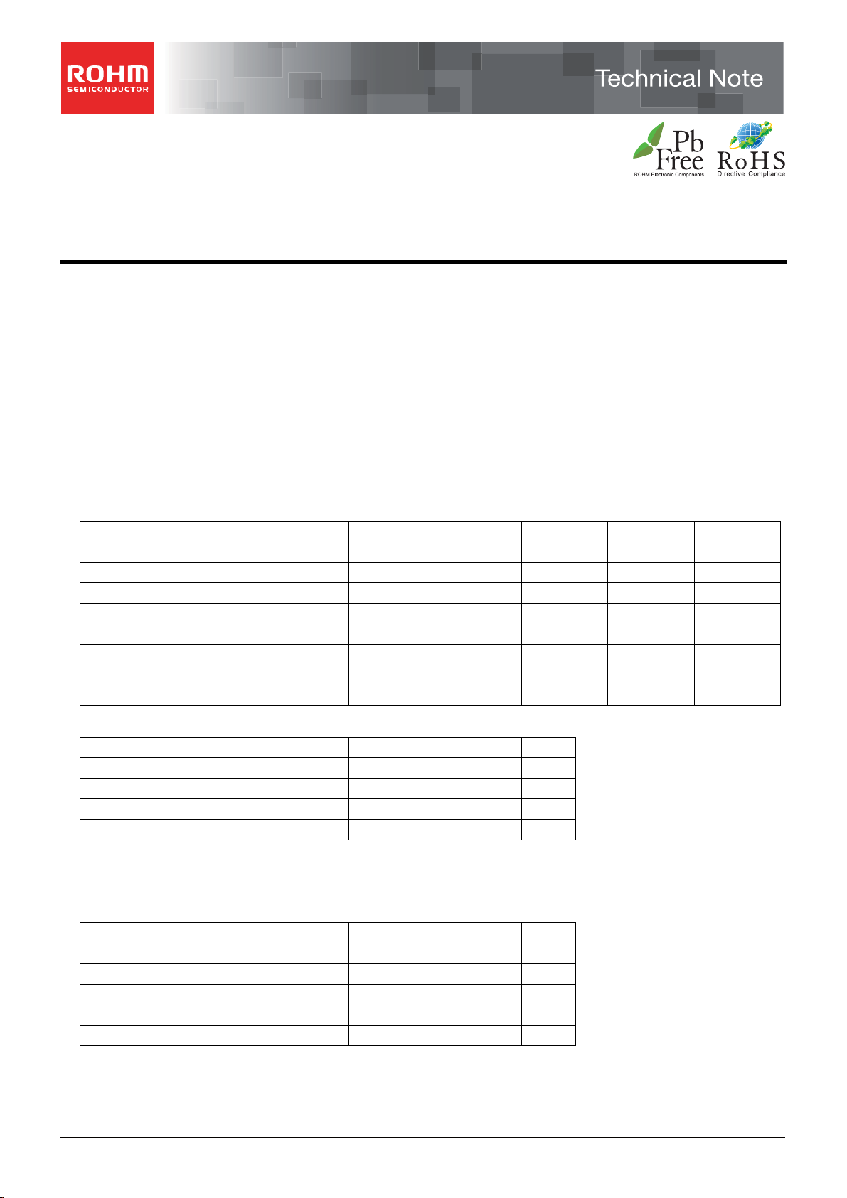
●Reference data (BU3071HFV basic data)
RBW:1kHz
VBW:100Hz
Technical Note
1V/div
5nsec/div
Fig.1 54MHz output waveform
(VDD=3.3V,CL=15pF,Ta=25℃)
●Reference data (BU3072HFV basic data)
1V/div
10nsec/div
Fig.4 27MHz output waveform
(VDD=3.3V,CL=15pF,Ta=25℃)
1V/div
500psec/div
Fig.2 54MHz Period-Jitter
(VDD=3.3V,CL=15pF,Ta=25℃)
1V/div
500psec/div
Fig.5 27MHz Period-Jitter
(VDD=3.3V,CL=15pF,Ta=25℃)
10dB/div
10kHz/div
Fig.3 54MHz spectrum
(VDD=3.3V,CL=15pF,Ta=25℃)
RBW:1kHz
VBW:100Hz
10dB/div
10kHz/div
Fig.6 27MHz spectrum
(VDD=3.3V,CL=15pF,Ta=25℃)
RBW:1kHz
VBW:100Hz
1V/div
5nsec/div
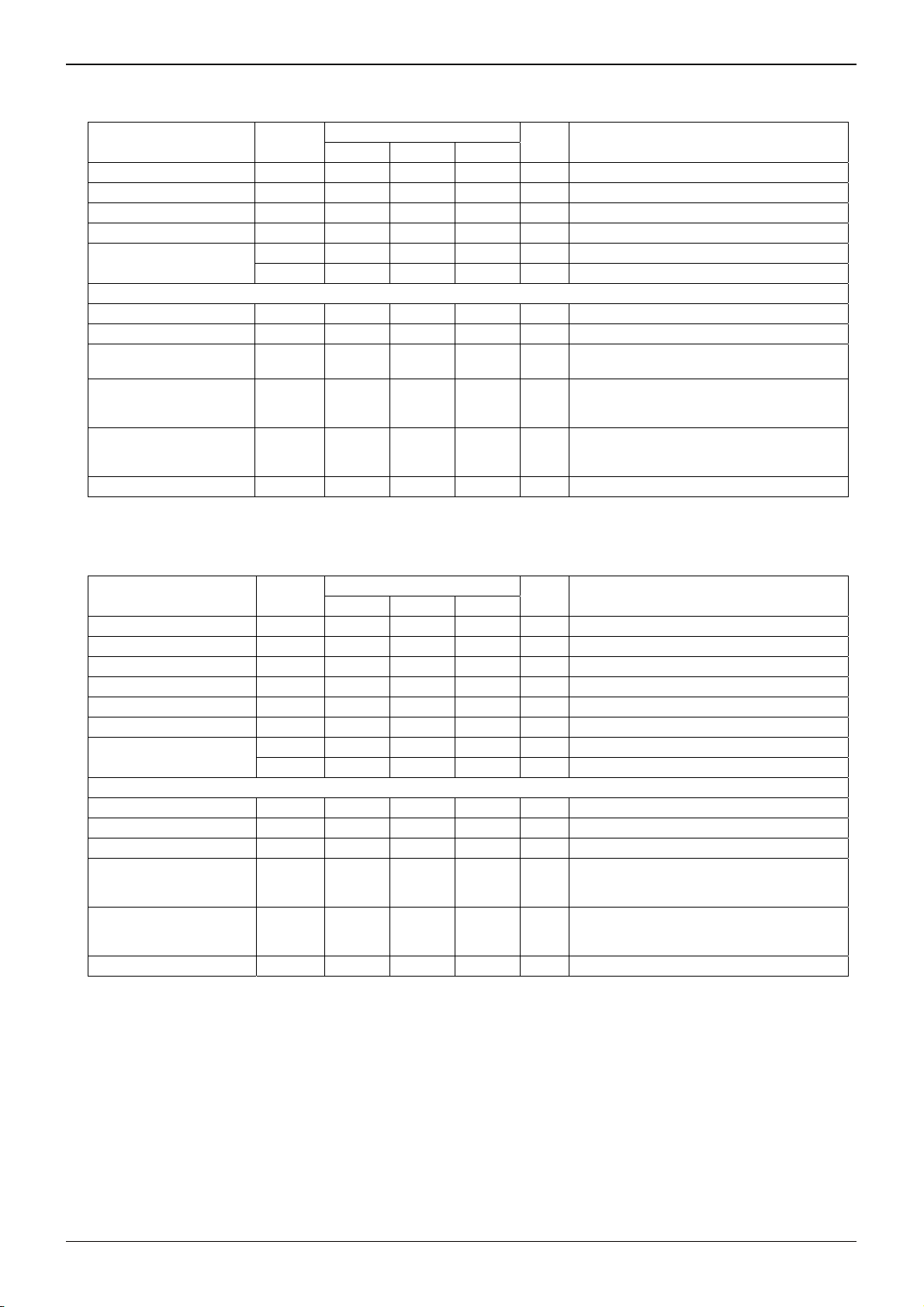
Fig.7 36MHz output waveform
(VDD=3.3V,CL=15pF,Ta=25℃)
1V/div
500psec/div
Fig.8 36MHz Period-Jitter
(VDD=3.3V,CL=15pF,Ta=25℃)
10dB/div
10kHz/div
Fig.9 36MHz spectrum
(VDD=3.3V,CL=15pF,Ta=25℃)
www.rohm.com
© 2009 ROHM Co., Ltd. All rights reserved.
5/21
2009.04 - Rev.A
Page 6
BU3071HFV,BU3072HFV,BU3073HFV,BU3076HFV,BU7322HFV,BU7325HFV
●Reference data (BU3073HFV basic data)
RBW:1kHz
VBW:100Hz
Technical Note
1V/div
10nsec/div
Fig.10 24.375MHz output waveform
(VDD=3.3V,CL=15pF,Ta=25℃)
1V/div
10nsec/div
Fig.13 24.5454MHz output waveform
(VDD=3.3V,CL=15pF,Ta=25℃)
●Reference data (BU3076HFV basic data)
1V/div
500psec/div
Fig.11 24.375MHz Period-Jitter
(VDD=3.3V,CL=15pF,Ta=25℃)
1V/div
500psec/div
Fig.14 24.5454MHz Period-Jitter
(VDD=3.3V,CL=15pF,Ta=25℃)
10dB/div
10kHz/div
Fig.12 24.375MHz spectrum
(VDD=3.3V,CL=15pF,Ta=25℃)
RBW:1kHz
VBW:100Hz
10dB/div
10kHz/div
Fig.15 24.5454MHz spectrum
(VDD=3.3V,CL=15pF,Ta=25℃
RBW:1kHz
VBW:100Hz
1V/div
5nsec/div
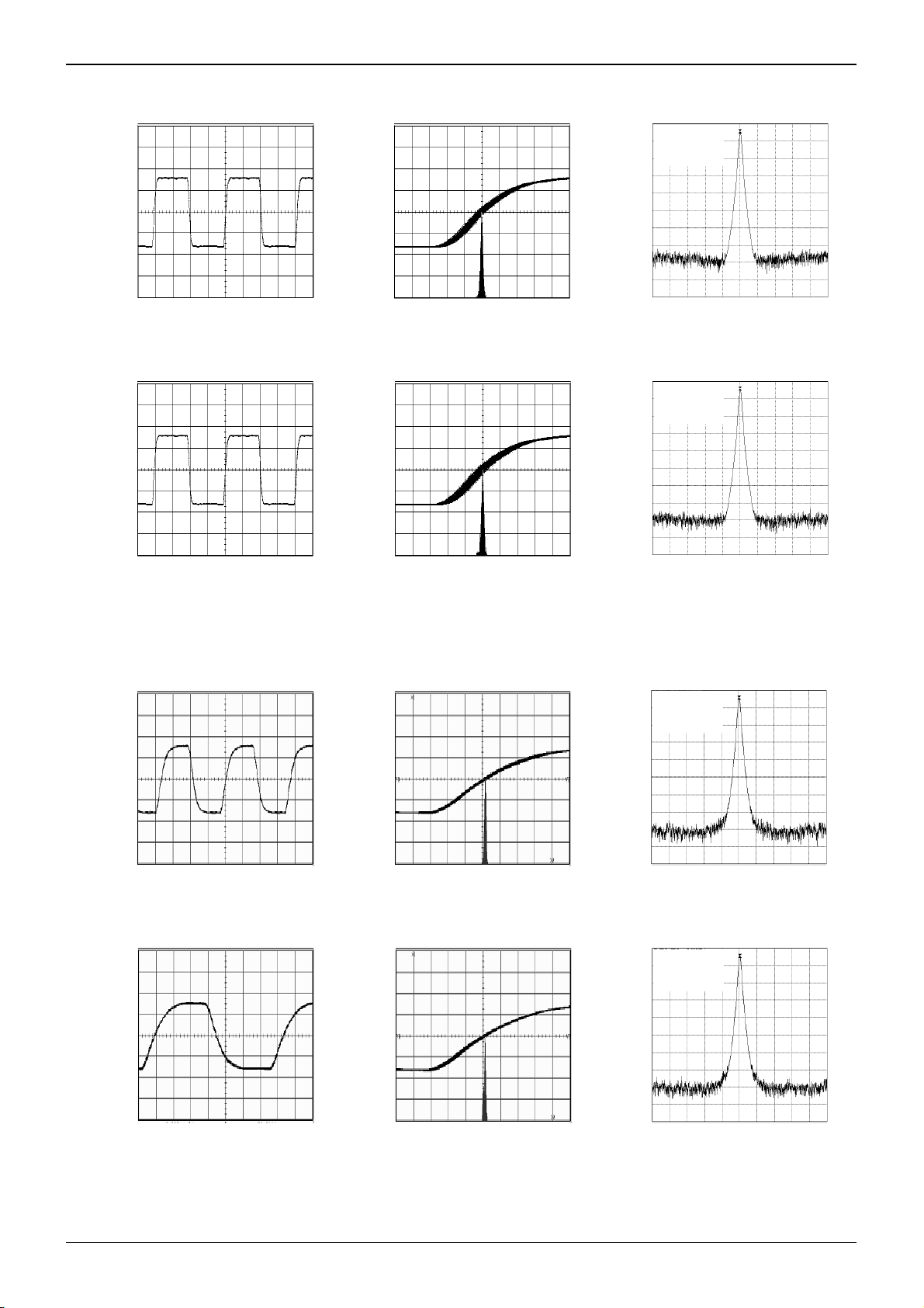
Fig.16 54MHz output waveform
(VDD=3.3V,CL=15pF,Ta=25℃)
1V/div
500psec/div
Fig.17 54MHz Period-Jitter
(VDD=3.3V,CL=15pF,Ta=25℃)
10dB/div
10kHz/div
Fig.18 54MHz spectrum
(VDD=3.3V,CL=15pF,Ta=25℃)
RBW:1kHz
VBW:100Hz
10dB/div
10kHz/div
Fig.21 67.5MHz spectrum
(VDD=3.3V,CL=15pF,Ta=25℃)
1V/div
2nsec/div
Fig.19 67.5MHz output waveform
(VDD=3.3V,CL=15pF,Ta=25℃)
1V/div
500psec/div
Fig.20 67.5MHz Period-Jitter
(VDD=3.3V,CL=15pF,Ta=25℃)
www.rohm.com
© 2009 ROHM Co., Ltd. All rights reserved.
6/21
2009.04 - Rev.A
Page 7
BU3071HFV,BU3072HFV,BU3073HFV,BU3076HFV,BU7322HFV,BU7325HFV
●Reference data (BU7322HFV basic data)
RBW:1kHz
VBW:100Hz
Technical Note
1V/div
5nsec/div
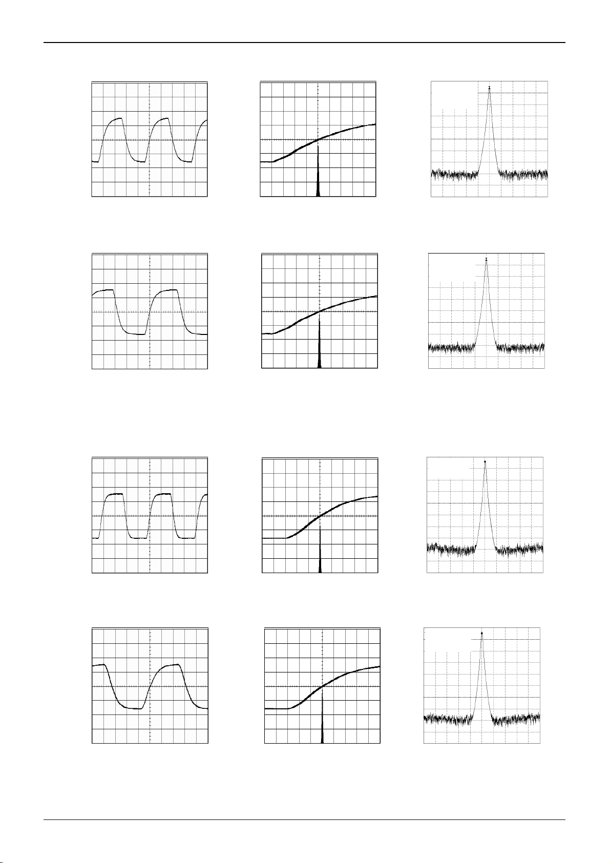
Fig.22 49.5MHz output waveform
(VDD=3.3V,CL=15pF,Ta=25℃)
1V/div
10nsec/div
Fig.25 36MHz output waveform
(VDD=3.3V,CL=15pF,Ta=25℃)
●Reference data (BU7325HFV basic data)
1V/div
500psec/div
Fig.23 49.5MHz Period-Jitter
(VDD=3.3V,CL=15pF,Ta=25℃)
1V/div
500psec/div
Fig.26 36MHz Period-Jitter
(VDD=3.3V,CL=15pF,Ta=25℃)
10dB/div
10kHz/div
Fig.24 49.5MHz spectrum
(VDD=3.3V,CL=15pF,Ta=25℃)
RBW:1kHz
VBW:100Hz
10dB/div
10kHz/div
Fig.27 36MHz spectrum
(VDD=3.3V,CL=15pF,Ta=25℃)
RBW:1kHz
VBW:100Hz
1V/div
5nsec/div
1V/div
500psec/div
10dB/div
10kHz/div
Fig.28 48MHz output waveform
(VDD=3.3V,CL=15pF,Ta=25℃)
Fig.29 48MHz Period-Jitter
(VDD=3.3V,CL=15pF,Ta=25℃)
Fig.30 48MHz spectrum
(VDD=3.3V,CL=15pF,Ta=25℃
RBW:1kHz
VBW:100Hz
1V/div
10nsec/div
1V/div
500psec/div
10dB/div
10kHz/div
Fig.31 78MHz output waveform
(VDD=3.3V,CL=15pF,Ta=25℃
Fig.32 78MHz Period-Jitter
(VDD=3.3V,CL=15pF,Ta=25℃)
Fig.33 78MHz spectrum
(VDD=3.3V,CL=15pF,Ta=25℃)
www.rohm.com
© 2009 ROHM Co., Ltd. All rights reserved.
7/21
2009.04 - Rev.A
Page 8

BU3071HFV,BU3072HFV,BU3073HFV,BU3076HFV,BU7322HFV,BU7325HFV
Technical Note
●Reference data (BU3071HFV Temperature and Supply voltage variations data)
55
54
53
52
51
50
49
48
Duty:Duty[%]
47
46
45
VDD=3.7V
VDD=2.9V
-25 0 25 50 75 100
temperature:T[℃]
VDD=3.3V
Fig.34 54MHz
Duty temperature characteristics
100
5
4
3
2
VDD=3.3V
Fall time:tf [nsec]
VDD=2.9V
1
0
-25 0 25 50 75 100
temperature:T [℃]
VDD=3.7V
Fig.35 54MHz
Rise-time temperature characteristics
600
5
4
3
2
VDD=2.9V
VDD=3.3V
Rise time:tr [nsec]
1
0
-25 0 25 50 75 100
temperature:T [℃]
VDD=3.7V
Fig.36 54MHz
Fall-time temperature characteristics
80
500
400
60
40
20
Period-Jitter 1σ:JsSD [psec]
VDD=3.7V
0
-25 0 25 50 75 100
VDD=3.3V
VDD=2.9V
temperature:T [℃]
Fig.37 54MHz Period-Jitter 1σ
temperature characteristics
300
200
100
Period-Jitter MIN-MAX:JsABS [psec]
VDD=2.9V
0
-25 0 25 50 75 100
temperature:T [℃]
Fig.38 54MHz Jitter-Min Max
temperature characteristics
=
VDD=3.3V
www.rohm.com
© 2009 ROHM Co., Ltd. All rights reserved.
8/21
2009.04 - Rev.A
Page 9

BU3071HFV,BU3072HFV,BU3073HFV,BU3076HFV,BU7322HFV,BU7325HFV
●Reference data (BU3072HFV Temperature and Supply voltage variations data)
55
54
53
52
51
50
49
Duty:Dyty [%]
48
47
46
45
-25 0 25 50 75 100
VDD=2.9V
temperature:T [℃]
VDD=3.7V
VDD=3.3V
Fig.39 27MHz Duty
temperature characteristics
5
4
3
2
Rise time:tr [nsec]
1
0
-25 0 25 50 75 100
VDD=2.9V
VDD=3.7V
temperature:T [℃]
VDD=3.3V
Fig.40 27MHz Rise-time
temperature characteristics
5
4
3
2
Fall time:tf [nsec]
1
0
-25 0 25 50 75 100
Fig.41 27MHz Fall-time
temperature characteristics
100
90
80
70
60
50
40
30
20
10
Period-Jitter 1σ:JsSD [psec]
55
54
53
52
51
50
49
48
Duty:Duty [%]
47
46
45
100
90
80
70
60
50
40
30
20
10
Period-Jitter 1σ:JsSD [psec]
VDD=3.7V
VDD=2.9V
0
-25 0 25 50 75 100
temperature:T [℃]
VDD=3.3V
Fig.42 27MHz Period-Jitter 1σ
temperature characteristics
VDD=3.7V
VDD=2.9V
VDD=3.3V
-25 0 25 50 75 100
temperature:T [℃]
Fig.44 36MHz Duty
temperature characteristic
VDD=2.9V
VDD=3.3V
VDD=3.7V
0
-25 0 25 50 75 100
temperature:T [℃]
Fig.47 36MHz Period-Jitter 1σ
temperature characteristic s
600
500
400
300
200
100
0
Period-Jitter MIN-MAX:JsABS [psec]
-25 0 25 50 75 100
VDD=2.9V
temperature:T [℃]
Fig.43 27MHz Jitter-MinMax
temperature characteristics
5
4
3
2
Rise time:tr [nsec]
1
0
-25 0 25 50 75 100
VDD=2.9V
VDD=3.7V
temperature:T [℃]
Fig.45 36MHz Rise-time
temperature characteristics
600
500
400
300
200
100
0
Period-Jitter MIN-MAX:JsABS [psec]
-25 0 25 50 75 100
VDD=2.9V
VDD=3.7V
temperature:T [℃]
Fig.48 36MHz Jitter-Min Max
temperature characteristics
VDD=3.7V
VDD=3.3V
VDD=3.3V
VDD=3.3V
5
4
3
2
Fall time:tf [nsec]
1
0
-25 0 25 50 75 100
Fig.46 36MHz Fall-time
temperature characteristics
Technical Note
VDD=2.9V
VDD=3.7V
temperature:T [℃]
VDD=2.9V
temperature:T [℃]
VDD=3.3V
VDD=3.7V
VDD=3.3V
www.rohm.com
© 2009 ROHM Co., Ltd. All rights reserved.
9/21
2009.04 - Rev.A
Page 10

BU3071HFV,BU3072HFV,BU3073HFV,BU3076HFV,BU7322HFV,BU7325HFV
Technical Note
●Reference data (BU3073HFV Temperature and Supply voltage variations data)
55
54
53
52
51
50
49
48
Duty:Duty [%]
47
46
45
-25 0 25 50 75 100
temperature:T [℃]
VDD=3.7V
VDD=3.3V
VDD=2.9V
Fig.49 24.375MHz Duty
temperature characteristics
100
90
80
Period-Jitter 1σ:JsSD [psec]
70
60
50
40
30
20
10
0
-25 0 25 50 75 100
temperature:T [℃]
VDD=3.7V
VDD=3.3V
VDD=2.9V
Fig.52 24.375MHz Period-Jitter 1σ
temperature characteristics
55
54
53
52
51
50
49
48
Duty:Duty [%]
47
46
45
VDD=2.9V VDD=3.3V
-25 0 25 50 75 100
temperature:T [℃]
VDD=3.7V
Fig.54 24.5454MHz Duty
temperature characteristics
100
90
80
70
60
50
40
30
20
10
Period-Jitter 1σ:JsSD [psec]
0
-25 0 25 50 75 100
temperature:T [℃]
VDD=2.9V
VDD=3.7V
VDD=3.3V
5
4
3
VDD=2.9V
2
Rise time:tr [nsec]
1
VDD=3.7V
0
-25 0 25 50 75 100
temperature:T [℃]
VDD=3.3V
Fig.50 24.375MHz Rise-time
temperature characteristics
600
500
400
300
[psec]
200
100
Period-Jitter MIN-MAX:JsABS
0
-25 0 25 50 75 100
VDD=3.7V
VDD=2.9V
temperature:T [℃]
VDD=3.3V
Fig.53 24.375MHz Jitter-Min Max
temperature characteristics
5
4
3
2
Rise time:tr [nsec]
1
0
VDD=3.7V
-25 0 25 50 75 100
temperature:T [℃]
VDD=2.9V
VDD=3.3V
Fig.55 24.5454MHz Rise-time
temperature characteristics
600
500
400
300
200
100
0
Period-Jitter MIN-MAX:JsABS [psec]
-25 0 25 50 75 100
VDD=3.7V
VDD=2.9V
temperature:T [℃]
VDD=3.3V
Fig.57 24.5454MHz Period-Jitter 1σ
temperature characteristics
Fig.58 24.5454MHz Jitter-MinMax
temperature characteristics
5
4
3
2
Fall time:tf [nsec)]
1
0
-25 0 25 50 75 100
VDD=2.9V
VDD=3.7V
temperature:T [℃]
VDD=3.3V
Fig.51 24.375MHz Fall-time
temperature characteristics
5
4
3
2
Fall time:tf [nsec]
1
0
VDD=3.7V
-25 0 25 50 75 100
temperature:T [℃]
VDD=2.9V
VDD=3.3V
Fig.56 24.5454MHz Fall-time
temperature characteristics
www.rohm.com
© 2009 ROHM Co., Ltd. All rights reserved.
10/21
2009.04 - Rev.A
Page 11

BU3071HFV,BU3072HFV,BU3073HFV,BU3076HFV,BU7322HFV,BU7325HFV
●Reference data (BU3076HFV Temperature and Supply voltage variations data)
Period-Jitter 1σ:JsSD [psec]
55
54
53
52
51
50
49
48
Duty:Duty [%]
47
46
45
-25 0 25 50 75 100
VDD=3.7V
VDD=2.9V
temperature:T [℃]
Fig.59 54MHz Duty
temperature characteristics
100
90
80
70
60
50
40
30
20
10
0
-25 0 25 50 75 100
VDD=2.9V
VDD=3.7V
temperature:T [℃]
VDD=3.3V
VDD=3.3V
5
4
3
2
Rise time:tr [nsec]
1
0
-25 0 25 50 75 100
VDD=2.9V
VDD=3.7V
temperature:T [℃]
Fig.60 54MHz Rise-time
temperature characteristics
600
500
400
300
200
100
0
Period-Jitter MIN-MAX:JsABS [psec]
-25 0 25 50 75 100
VDD=2.9V
VDD=3.7V
temperature:T [℃]
VDD=3.3V
VDD=3.3V
5
4
3
2
Fall time:tf [nsec]
1
0
VDD=3.7V
-25 0 25 50 75 100
Fig.61 54MHz Fall-time
temperature characteristics
Duty:Duty [%]
Period-Jitter 1σ:JsSD [psec]
Fig.62 54MHz Period-Jitter 1σ
temperature characteristics
55
54
53
52
51
50
49
48
47
46
45
-25 0 25 50 75 100
VDD=3.3V
temperature:T [℃]
VDD=3.7V
VDD=2.9V
Fig.64 67.5MHz
Duty temperature characteristics
70
60
50
40
30
20
10
0
-25 0 25 50 75 100
VDD=2.9V
VDD=3.7V
temperature:T [℃]
VDD=3.3V
Fig.67 67.5MHz Period-Jitter 1σ
temperature characteristics
Fig.63 54MHz Jitter-Min Max
temperature characteristics
5
4
3
2
Rise time:tr [nsec]
1
0
-25 0 25 50 75 100
VDD=2.9V
temperature:T [℃]
VDD=3.3V
VDD=3.7V
Fig.65 67.5MHz
Rise-time temperature characteristics
600
500
400
300
200
100
0
Period-Jitter MIN-MAX:JsABS [psec]
VDD=2.9V
-25 0 25 50 75 100
temperature:T [℃]
VDD=3.7V
VDD=3.3V
Fig.68 67.5MHz Jitter-MinMax
temperature characteristics
5
4
3
2
Fall time:tf [nsec]
1
0
-25 0 25 50 75 100
Fig.66 67.5MHz
Fall-time temperature characteristics
Technical Note
VDD=2.9V
VDD=3.3V
tem perature:T [℃]
VDD=2.9V
VDD=3.7V
temperature:T [℃]
VDD=3.3V
www.rohm.com
© 2009 ROHM Co., Ltd. All rights reserved.
11/21
2009.04 - Rev.A
Page 12

BU3071HFV,BU3072HFV,BU3073HFV,BU3076HFV,BU7322HFV,BU7325HFV
Technical Note
●Reference data (BU7322HFV Temperature and Supply voltage variations data)
55
54
53
52
51
50
49
48
Duty:Duty [%]
47
46
45
-25 0 25 50 75 100
VDD=3.7V
VDD=2.75V
temperature: T [℃]
Fig.69 49.5MHz Duty
temperature characteristics
100
90
80
70
60
50
40
30
20
10
Period-Jitter 1σ:JsSD [psec]
0
-25 0 25 50 75 100
VDD=3.7V
temperature:T [℃]
Fig.72 49.5MHz Period-Jitter 1σ
temperature characteristics
55
54
53
Duty:Duty [%]
52
51
50
49
48
47
46
45
VDD=3.7V
VDD=2.75V
-25 0 25 50 75 100
temperature:T [℃]
Fig.74 36MHz Duty
temperature characteristics
70
60
50
40
30
20
Period-Jitter 1σ:JsSD [psec]
10
0
VDD=3.3V
-25 0 25 50 75 100
temperature:T [℃]
Fig.77 36MHz Period-Jitter 1σ
temperature characteristics
VDD=3.3V
VDD=2.75V
VDD=3.3V
VDD=3.3V
VDD=2.75V
VDD=3.7V
5
4
3
2
Rise time:tr [nsec]
1
0
-25 0 25 50 75 100
VDD=2.75V
VDD=3.7V
temperature:T [℃]
Fig.70 49.5MHz Rise-time
temperature characteristics
600
500
400
300
200
100
0
Period-Jitter MIN-MAX:JsABS [psec]
VDD=3.7V
VDD=3.3V
-25 0 25 50 75 100
temperature:T [℃]
Fig.73 49.5MHz Jitter-Min Max
temperature characteristics
5
4
3
2
Rise time:tr [nsec]
1
0
-25 0 25 50 75 100
VDD=2.75V
VDD=3.7V
temperature:T [℃]
Fig.75 36MHz Rise-time
temperature characteristics
600
500
400
300
[psec]
200
100
Period-Jitter MIN-MAX:JsABS
0
-25 0 25 50 75 100
VDD=3.3V
temperature:T [℃]
Fig.78 36MHz Jitter-MinMax
temperature characteristics
VDD=3.3V
VDD=2.75V
VDD=3.3V
VDD=2.75V
VDD=3.7V
5
4
3
2
Fall time:tf [nsec]
1
0
-25 0 25 50 75 100
VDD=2.75V
VDD=3.7V
tem perature:T [℃]
VDD=3.3V
Fig.71 49.5MHz Fall-time
temperature characteristics
5
4
3
2
Fall time:tf [nsec]
1
0
-25 0 25 50 75 100
VDD=2.75V
VDD=3.7V
temperature:T [℃]
VDD=3.3V
Fig.76 36MHz Fall-time
temperature characteristics
www.rohm.com
© 2009 ROHM Co., Ltd. All rights reserved.
12/21
2009.04 - Rev.A
Page 13

BU3071HFV,BU3072HFV,BU3073HFV,BU3076HFV,BU7322HFV,BU7325HFV
Technical Note
●Reference data (BU7325HFV Temperature and Supply voltage variations data)
55
54
53
52
51
50
49
48
Duty:Duty [%]
47
46
45
100
90
80
70
60
50
40
30
20
10
Period-Jitter 1σ:JsSD [psec]
0
-25 0 25 50 75 100
55
54
53
52
51
50
49
48
Duty:Duty [%]
47
46
45
70
60
50
40
30
20
10
Period-Jitter 1σ:JsSD [psec]
0
VDD=3.7V
VDD=3.3V
-25 0 25 50 75 100
temperature:T [℃]
VDD=2.75V
Fig.79 48MHz
Duty temperature characteristics
VDD=2.75V
VDD=3.3V
temperature:T [℃]
VDD=3.7V
Fig.82 48MHz Period-Jitter 1σ
temperature characteristics
VDD=3.7V
VDD=3.3V
-25 0 25 50 75 100
temperature:T [℃]
VDD=2.75V
Fig.84 78MHz Duty
temperature characteristics
VDD=2.75V
VDD=3.3V
-25 0 25 50 75 100
temperature:T [℃]
VDD=3.7V
Fig.87 78MHz Period-Jitter 1σ
temperature characteristics
5
4
3
2
Rise time:tr [nsec]
1
0
-25 0 25 50 75 100
VDD=3.7V
VDD=3.3V
VDD=2.75V
temperature:T [℃]
Fig.80 48MHz
Rise-time temperature characteristics
600
500
400
VDD=3.3V
VDD=3.7V
-25 0 25 50 75 100
Period-Jitter MIN-MAX:JsABS [psec]
300
200
100
0
VDD=2.75V
temperature:T [℃]
Fig.83 48MHz Jitter-Min Max
temperature characteristics
5
4
3
2
Rise time:tr [nsec]
1
0
-25 0 25 50 75 100
VDD=2.75V
VDD=3.3V
temperature:T [℃]
VDD=3.7V
Fig.85 78MHz Rise-time
temperature characteristics
600
500
400
300
200
100
0
Period-Jitter MIN-MAX:JsABS [psec]
VDD=2.75V
-25 0 25 50 75 100
temperature:T [℃]
VDD=3.3V
VDD=3.7V
Fig.88 78MHz Jitter-MinMax
temperature characteristic
5
4
3
2
Fall time:tf [nsec]
1
0
-25 0 25 50 75 100
temperature:T [℃]
VDD=2.75V
VDD=3.7V
VDD=3.3V
Fig.81 48MHz
Fall-time temperature characteristics
5
4
3
VDD=2.75V
2
Fall time:tf [nsec]
1
0
VDD=3.3V
-25 0 25 50 75 100
temperature:T [℃]
VDD=3.7V
Fig.86 78MHz Fall-time
temperature characteristics
www.rohm.com
© 2009 ROHM Co., Ltd. All rights reserved.
13/21
2009.04 - Rev.A
Page 14

BU3071HFV,BU3072HFV,BU3073HFV,BU3076HFV,BU7322HFV,BU7325HFV
●Block diagram, pin assignment/functions
(BU3071HFV)
1:VDD
2:VSS
6:
5:
IN
TEST
6pin:IN
PLL
1/4
3:OUT
4:
OE
4pin:OE
Fig.89 Fig.90
PIN
NO.
PIN
name
Function
1 VDD Power supply
2 VSS GND
3 OUT Clock output terminal
4 OE Output enable (L: disable, H: enable), equipped with Pull-down function, output fixed to L at disable
5 TEST TEST pin, equipped with Pull-down function
6 IN Clock input pin (28.6363 MHz input)
(BU3072HFV)
1:VDD
2:VSS
3:OUT
IN
6:
SEL
5:
4:PD
6pin:IN
5pin:SEL
PLL
DATA1
DATA2
1/4
4pin:P D
PIN
NO.
1 VDD
2 VSS
3 OUT
4 PD
5 SEL
6 IN
Fig.91
PIN
name
Fig.92
Function
Power supply
GND
Clock output terminal (L:27.0000MHz, H:36.0000MHz)
Power-down (L: Hi-Z, H: enable), equipped with Pull-down function, output set to Hi-Z at disable
Output selection (L: 27.0000 MHz, H: 36.0000 MHz)
Clock input pin (48.0000 MHz input)
(BU3073HFV)
1:VDD
2:VSS
3:OUT
Fig.93
IN
6:
SEL
5:
4:PD
6pin:IN
5pin:SEL
4pin:PD
PLL
DATA1
DATA2
1/8
Fig.94
PIN
NO.
1 VDD
2 VSS
3 OUT
4 PD
5 SEL
6 IN
PIN
name
Function
Power supply
GND
Clock output terminal (L:24.3750MHz, H:24.5454MHz)
Power-down (L: disable, H: enable), equipped with Pull-down function, output set to L at disable
Output selection (L:24.3750MHz, H:24.5454MHz)
Clock input pin (48.0000MHz input)
Technical Note
3pin:OUT
3pin: OUT
3pin:OUT
www.rohm.com
© 2009 ROHM Co., Ltd. All rights reserved.
14/21
2009.04 - Rev.A
Page 15

BU3071HFV,BU3072HFV,BU3073HFV,BU3076HFV,BU7322HFV,BU7325HFV
(BU3076HFV)
1:VD D
2:VSS
3:OU T
6:IN
5:SEL
4:OE
PIN
NO.
1 VDD
2 VSS
3 OUT
4 OE
5 SEL
6 IN
Fig.95 Fig.96
PIN
name
Power supply
GND
Clock output terminal (L:54.0000MHz, H:67.5000MHz)
Power-down (L: disable, H: enable), equipped with Pull-down function, output set to L at disable
Output selection (L:54.0000MHz, H:67.5000MHz)
Clock input pin (27.0000MHz input)
6pin:IN
5pin:SEL
4pin:OE
Function
PLL
DATA1
DATA2
1/4
(BU7322HFV)
1:VD D
2:VSS
3:OU T
6:IN
5:SEL
4:OE
6pin:IN
5pin:SEL
PLL
DATA1
DATA2
1/6
1/8
4pin:OE
PIN
NO.
1
2
3
4
5
6
Fig.97
PIN
name
VDD
VSS
OUT
OE
SEL
IN
Fig.98
Function
Power supply
GND
Clock output terminal (L:49.5000MHz, H:36.0000MHz)
Power-down (L:disable ,H:enable) equipped with Pull-down function, disable output set to L at disable
Output selection (L:49.5000MHz, H:36.0000MHz) equipped with Pull-down function
Clock input pin (27.0000MHz input)
(BU7325HFV)
1:VD D
2:VSS
3:OU T
6:IN
5:SEL
4:OE
6pin:IN
5pin:SEL
PLL
DATA1
DATA2
1/6
1/4
PIN
NO.
1
2
3
4
5
6
Fig.99
PIN
name
VDD Power supply
VSS GND
OUT Clock output terminal (L:48.0000MHz, H:78.0000MHz)
OE Power-down (L:disable ,H:enable) equipped with Pull-down function, disable output set to L at disable
SEL Output selection (L:48.0000MHz, H:78.0000MHz)
IN Clock input pin (27.0000MHz input)
4pin:OE
Fig.100
Function
Technical Note
3pin:OUT
3pin:OUT
3pin:OUT
www.rohm.com
© 2009 ROHM Co., Ltd. All rights reserved.
15/21
2009.04 - Rev.A
Page 16

BU3071HFV,BU3072HFV,BU3073HFV,BU3076HFV,BU7322HFV,BU7325HFV
Technical Note
●Application circuit example
(BU3071HFV) (BU3072HFV)
54.0000MHz
1:VDD
2:VSS
3:OUT
Fig.101
6:
5:
4:
IN
TEST
OE
28.6363MHz
H:enable
L:disable
H:36.0000MHz
L:27.0000MHz
1:VDD
2:VSS
3:OUT
6:
5:
4:
Fig.102
IN
SEL
PD
48MHz
H:36.0000MHz
L:27.0000MHz
H:enable
L:Hi-Z
(BU3073HFV) (BU3076HFV)
H:24.5454MHz
L:24.3750MHz
1:VDD
2:VSS
3:OUT
6:
5:
4:
SEL
PD
H:24.5454MHz
L:24.3750MHz
48MHz
IN
Fig.103 Fig.104
H:enable
L:disable
H:67.5000MHz
L:54.00000MHz
27MHz
1:VDD
2: VSS
3: OUT
6: IN
5: SEL
4: OE
H:67.5000MHz
L:54.0000MHz
H:enable
L:disable
(BU7322HFV) (BU7325HFV)
H:36.0000MHz
L:49.5000MHz
27MHz
1:VDD
2: VSS
3: OUT
6: IN
5: SEL
4: OE
Fig.105 Fig.106
H:36.0000MHz
L:49.5000MHz
H:enable
L:disable
H:78.0000MHz
L:48.0000MHz
1:VDD
2: VSS
3: OUT
6: IN
5: SEL
4: OE
27MHz
H:78.0000MHz
L:48.0000MHz
H:enable
L:disable
For VDD and VSS, insert a bypass capacitor of approx. 0.1 µF as close as possible to the pin.
Bypass capacitors with good high-frequency characteristics are recommended.
Even though we believe that the typical application circuit is worth of a recommendation, please be sure to thoroughly recheck the characteristics before use.
www.rohm.com
© 2009 ROHM Co., Ltd. All rights reserved.
16/21
2009.04 - Rev.A
Page 17

BU3071HFV,BU3072HFV,BU3073HFV,BU3076HFV,BU7322HFV,BU7325HFV
●Equivalent circuit
3-pin (Output pin)
4-pin (Input pin)
Fig.107
BU3071HFV, BU3073HFV, BU3076HFV
BU7322HFV, BU7325HFV
Fig.109
From the inside of IC
Fig.108
BU3072HFV
To the inside of IC
Technical Note
From the inside of IC
PD=L ; Hi-Z
; enable
www.rohm.com
© 2009 ROHM Co., Ltd. All rights reserved.
17/21
2009.04 - Rev.A
Page 18

BU3071HFV,BU3072HFV,BU3073HFV,BU3076HFV,BU7322HFV,BU7325HFV
5-pin (Input pin)
BU3072HFV, BU3073HFV, BU3076HFV
6-pin (Input pin)
Fig.110
BU7322HFV, BU7325HFV
To the inside
of IC
To the inside
of IC
Fig.112
BU3072HFV, BU3073HFV, BU3076HF
BU7322HFV, BU7325HFV
To the inside of IC
To the inside of IC
Fig .111
BU3071HFV
From the inside of IC
To the inside of IC
To the inside of IC
Fig.113
BU3071HFV
Technical Note
www.rohm.com
© 2009 ROHM Co., Ltd. All rights reserved.
18/21
2009.04 - Rev.A
Page 19

BU3071HFV,BU3072HFV,BU3073HFV,BU3076HFV,BU7322HFV,BU7325HFV
●Appearance of Marker
3.0±0.1
0.75MAX
・List of markers
2.6±0.1
Model name Marker
BU3071HFV AB
BU3072HFV AC
BU3073HFV AD
BU3076HFV AA
BU7322HFV AE
BU7325HFV AH
(Dimension including burr: Max. 1.8)
1.6±0.1
○ ○
(Dimension including burr: Max. 2.8)
0.5
0.22±0.05
Marker
LOT No.
Fig.114
(1.2)
(1.4)
(0.45)
(1.5)
(0.15)
(UNIT:mm)
Technical Note
0.145±0.05
www.rohm.com
© 2009 ROHM Co., Ltd. All rights reserved.
19/21
2009.04 - Rev.A
Page 20

BU3071HFV,BU3072HFV,BU3073HFV,BU3076HFV,BU7322HFV,BU7325HFV
●Notes for use
1) Absolute Maximum Ratings
An excess in the absolute maximum ratings, such as applied voltage (VDD or VIN), operating temperature range (Topr),
etc., can break down devices, thus making impossible to identify breaking mode such as a short circuit or an open circuit.
If any special mode exceeding the absolute maximum ratings is assumed, consideration should be given to take physical
safety measures including the use of fuses, etc.
2) Recommended operating conditions
These conditions represent a range within which characteristics can be provided approximately as expected. The
electrical characteristics are guaranteed under the conditions of each parameter.
3) Reverse connection of power supply connector
The reverse connection of power supply connector can break down ICs. Take protective measures against the breakdown
due to the reverse connection, such as mounting an external diode between the power supply and the IC’s power supply
terminal.
4) Power supply line
Design PCB pattern to provide low impedance for the wiring between the power supply and the GND lines.
In this regard, for the digital block power supply and the analog block power supply, even though these power supplies has
the same level of potential, separate the power supply pattern for the digital block from that for the analog block, thus
suppressing the diffraction of digital noises to the analog block power supply resulting from impedance common to the
wiring patterns. For the GND line, give consideration to design the patterns in a similar manner.
Furthermore, for all power supply terminals to ICs, mount a capacitor between the power supply and the GND terminal. At
the same time, in order to use an electrolytic capacitor, thoroughly check to be sure the characteristics of the capacitor to
be used present no problem including the occurrence of capacity dropout at a low temperature, thus determining the
constant.
5) GND voltage
Make setting of the potential of the GND terminal so that it will be maintained at the minimum in any operating state.
Furthermore, check to be sure no terminals are at a potential lower than the GND voltage including an actual electric transient.
6) Short circuit between terminals and erroneous mounting
In order to mount ICs on a set PCB, pay thorough attention to the direction and offset of the ICs. Erroneous mounting can
break down the ICs. Furthermore, if a short circuit occurs due to foreign matters entering between terminals or between
the terminal and the power supply or the GND terminal, the ICs can break down.
7) Operation in strong electromagnetic field
Be noted that using ICs in the strong electromagnetic field can malfunction them.
8) Inspection with set PCB
On the inspection with the set PCB, if a capacitor is connected to a low-impedance IC terminal, the IC can suffer stress.
Therefore, be sure to discharge from the set PCB by each process. Furthermore, in order to mount or dismount the set
PCB to/from the jig for the inspection process, be sure to turn OFF the power supply and then mount the set PCB to the jig.
After the completion of the inspection, be sure to turn OFF the power supply and then dismount it from the jig. In addition,
for protection against static electricity, establish a ground for the assembly process and pay thorough attention to the
transportation and the storage of the set PCB.
9) Input terminals
In terms of the construction of IC, parasitic elements are inevitably formed in relation to potential. The operation of the
parasitic element can cause interference with circuit operation, thus resulting in a malfunction and then breakdown of the
input terminal. Therefore, pay thorough attention not to handle the input terminals, such as to apply to the input terminals a
voltage lower than the GND respectively, so that any parasitic element will operate. Furthermore, do not apply a voltage to
the input terminals when no power supply voltage is applied to the IC. In addition, even if the power supply voltage is
applied, apply to the input terminals a voltage lower than the power supply voltage or within the guaranteed value of
electrical characteristics.
10) Ground wiring pattern
If small-signal GND and large-current GND are provided, It will be recommended to separate the large-current GND
pattern from the small-signal GND pattern and establish a single ground at the reference point of the set PCB so that
resistance to the wiring pattern and voltage fluctuations due to a large current
small-signal GND. Pay attention not to cause fluctuations in the GND wiring pattern of external parts as well.
11) External capacitor
In order to use a ceramic capacitor as the external capacitor, determine the constant with consideration given to a
degradation in the nominal capacitance due to DC bias and changes in the capacitance due to temperature, etc.
will cause no fluctuations in voltages of the
Technical Note
www.rohm.com
© 2009 ROHM Co., Ltd. All rights reserved.
20/21
2009.04 - Rev.A
Page 21

BU3071HFV,BU3072HFV,BU3073HFV,BU3076HFV,BU7322HFV,BU7325HFV
●Ordering part number
B U 3 0 7 1 H F V - T R
Technical Note
Part No. Part No.
HVSOF6
1.6±0.1
(MAX 1.8 include BURR)
456
0.1
3.0±0.1
2.6±
(MAX 2.8 include BURR)
0.75Max.
(1.2)
(1.4)
321
S
0.1 S
0.22±0.05
0.5
3071,3072,3073
3076,7322,7325
(1.5)
(0.45)
(0.15)
0.145±0.05
(Unit : mm)
Package
HFV : HVSOF6
<Tape and Reel information>
Embossed carrier tapeTape
Quantity
Direction
of feed
3000pcs
TR
The direction is the 1pin of product is at the upper right when you hold
()
reel on the left hand and you pull out the tape on the right hand
Reel
Packaging and forming specification
TR: Embossed tape and reel
1pin
Direction of feed
Order quantity needs to be multiple of the minimum quantity.
∗
www.rohm.com
© 2009 ROHM Co., Ltd. All rights reserved.
21/21
2009.04 - Rev.A
Page 22

Notes
No copying or reproduction of this document, in part or in whole, is permitted without the
consent of ROHM Co.,Ltd.
The content specied herein is subject to change for improvement without notice.
The content specied herein is for the purpose of introducing ROHM's products (hereinafter
"Products"). If you wish to use any such Product, please be sure to refer to the specications,
which can be obtained from ROHM upon request.
Examples of application circuits, circuit constants and any other information contained herein
illustrate the standard usage and operations of the Products. The peripheral conditions must
be taken into account when designing circuits for mass production.
Great care was taken in ensuring the accuracy of the information specied in this document.
However, should you incur any damage arising from any inaccuracy or misprint of such
information, ROHM shall bear no responsibility for such damage.
The technical information specied herein is intended only to show the typical functions of and
examples of application circuits for the Products. ROHM does not grant you, explicitly or
implicitly, any license to use or exercise intellectual property or other rights held by ROHM and
other par ties. ROHM shall bear no responsibility whatsoever for any dispute arising from the
use of such technical information.
Notice
The Products specied in this document are intended to be used with general-use electronic
equipment or devices (such as audio visual equipment, ofce-automation equipment, communication devices, electronic appliances and amusement devices).
The Products specied in this document are not designed to be radiation tolerant.
While ROHM always makes efforts to enhance the quality and reliability of its Products, a
Product may fail or malfunction for a variety of reasons.
Please be sure to implement in your equipment using the Products safety measures to guard
against the possibility of physical injury, re or any other damage caused in the event of the
failure of any Product, such as derating, redundancy, re control and fail-safe designs. ROHM
shall bear no responsibility whatsoever for your use of any Product outside of the prescribed
scope or not in accordance with the instruction manual.
The Products are not designed or manufactured to be used with any equipment, device or
system which requires an extremely high level of reliability the failure or malfunction of which
may result in a direct threat to human life or create a risk of human injury (such as a medical
instrument, transportation equipment, aerospace machiner y, nuclear-reactor controller,
fuel-controller or other safety device). ROHM shall bear no responsibility in any way for use of
any of the Products for the above special purposes. If a Product is intended to be used for any
such special purpose, please contact a ROHM sales representative before purchasing.
If you intend to export or ship overseas any Product or technology specied herein that may
be controlled under the Foreign Exchange and the Foreign Trade Law, you will be required to
obtain a license or permit under the Law.
www.rohm.com
© 2009 ROHM Co., Ltd. All rights reserved.
Thank you for your accessing to ROHM product informations.
More detail product informations and catalogs are available, please contact us.
ROHM Customer Support System
http://www.rohm.com/contact/
R0039
A
 Loading...