

Page 1
1
Video ICs
Digital servo controller for VCRs
BU2880 series
The BU2880 series are linear digital-servo controllers that allow construction of a VCR servo system using one IC.
The DRUM and CAPSTAN systems have digital filters, and the IC is compatible with VISS / VASS overwriting and
wide-aspect operation.
•
Applications
Video cassette recorders
•
Absolute maximum ratings (Ta = 25°C)
Parameter
Symbol Limits Unit
7.0 V
Pd mW
Topr °C
Tstg °C
V
DD
500
∗
– 15 ~ + 70
– 55 ~ + 125
Power supply voltage
Power dissipation
Operating temperature
Storage temperature
∗
Reduced by 5mW for each increase in Ta of 1°C over 25°C.
•
Features
1) All VCR servo functions on a single chip.
2) Digital filters in the DRUM and CAPSTAN speed and
phase systems.
3) Built-in CTL amplifier with serial gain setting.
4) VISS / VASS overwriting and INDEX detection func-
tions for wide-aspect operation.
5) DRUM f
H compensation calculation function from
speed detect function.
6) 6.5H discrimination.
7) Compatible with 19µm heads.
•
Recommended operating conditions (Ta = 25°C)
Parameter Symbol Min. Typ. Max. Unit
VV
DD
4.5 5.0 5.5Power supply voltage
查询BU2880 series供应商
Page 2
2
Video ICs BU2880 series
•
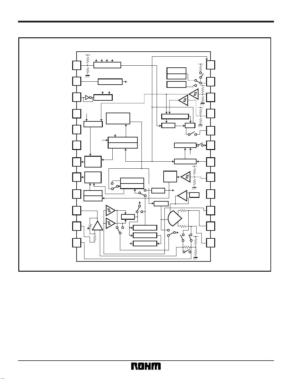
Block diagram
1
2
3
4
5
6
7
8
9
10
11
12
19
20
21
22
23
24
18
17
16
15
14
13
CTL COUNT
SEARCH DET
DRUM ROM CAL
CAP REF
CAP TRAPE
ROM
CAPFV
FF
DIGITAL
FILTER
DIGITAL
FILTER
+ MIX
+ MIX
RECCTL
1 / M
R2R
– +
F
F
ROMDATA
R
R
REC
REC
CTLOUT1
∗
1FWD
SAMPLE
SAMPLE
CTLOUT2
TRIG
HIGH
TRIG
CFGOUT
CFG
COUNT
VP DELAY
VP WIDTH
VFF
H
VPON
AHSWON
PGMM
FG COUNTER
(SERVOFF)
CK R
DPG
ROMDATA
ROMDATA
VD
P.SET
SAMPLE
SAMPLE
DRUMFV
TRA MM +
CTL DELAY
REF COUNTER
DRUM TRAPE
FSC
BIT PAT.
PWMGEN
VD
SYNC SEP
SIDATA DET
MODE
DFG
DUTY DET
VISS DET
6.5H DET
6.5H
SDATA
VSYNCIN
FSCIN
CFGOUT
CTLOUT1
CTLOUT2
DRUMPFV
CAPPFV
V
DD
CTLAMPOUT
CTLAMP
–
CTLAMP
+
VHSW
CTLDUTY
DFGIN
DPGIN
AHSW
VHPULSE
VPDLY
CFGIN
VSS
CTLCOMPIN
RECCTL
+
RECCTL
–
+
–
REC
Page 3
3
Video ICs BU2880 series
•
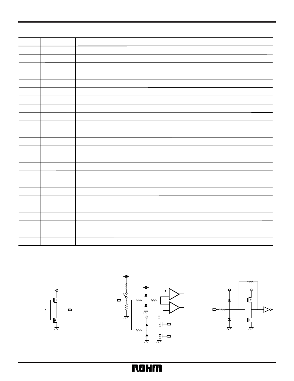
Pin descriptions
Pin No.
1 SDATA
2 VSYNCIN
3 FSCIN
4 CFGOUT
5 CTLOUT1
6 CTLOUT2
7 DRUMPFV
8 CAPPFV
9
10 CTLAMPOUT
11 CTLAMP
–
12 CTLAMP
+
13 RECCTL
–
14 RECCTL
+
15 CTLCOMPIN
16 VSS
17 CFGIN
18 VPDLY
19 VHPULSE
20 AHSW
21 DPGIN
22 DFGIN
23 CTLDUTY
24 VHSW
V
DD
Pin name Function
Serial data input (tri-state)
Composite sync input
System clock input
CFG divider output
CTL comparator output
CTL divider output
DRUM control output (digital filter output)
CAPSTAN control output (digital filter output)
Power supply
CTLAMP output
CTLAMP – input
CTLAMP + input
Recording CTL – output
Recording CTL + output
CTL comparator input
GND
CFG input
Quasi-VH pulse delay amount control input
Quasi-VH pulse output
Head switch audio output
DRUM PG input
DRUM FG input
Duty discrimination, VISS discrimination, 6.5H discrimination output / VASS duty control input
HEAD SW video output
•
Input / output circuits
OUT
4: CFGOUT
5: CTLOUT1
6: CTLOUT2
7: DRUMPFV
8: CAPPFV
20: AHSW
24: VHSW
Logic output
+
+
60k
60k
2k
500
1.5 / 5V
DD
1 / 5VDD
45
INIOP
INION
IN
23: CTLDUTY
Shared input / output terminal
DUTY I / O: OFF
6.5H discrimination: ON
–
–
420
FSCIN
52k
3: FSCIN
FSC input
Page 4

4
Video ICs BU2880 series
VPOUT
60k
60k
19: VHPULSE
Tri-state output
+
+
2k
3 / 5V
DD
2 / 5VDD
500
IN
2: VSYNCIN
18: VPDLY
–
–
Two-value input
+
+
+
+
2k
3 / 5V
DD
3.5 / 5VDD
1.5 / 5VDD
1 / 5VDD
500
IN
60k
60k
1: SDATA
–
–
–
–
Three-value input
2k
2.75 / 5V
DD
2.25 / 5VDD
2.5 / 5VDD
500
+
+
+
CFGIN
36k
36k
17: CFGIN
–
–
–
CFG input (zero cross comparator)
+
+
+
+
22.5
2.35 / 5V
DD
2.65 / 5VDD
2.75 / 5VDD
2.25 / 5VDD
CTLCOHPIN
15: CTLCOMP IN
–
–
–
–
CTL comparator input
23k
23k
+
CTLAMPOUT
42k
CTLAMP
+
CTLAMP
_
RECCTL
–
RECCTL
+
10: CTLAMPOUT
11: CTLAMP
–
12: CTLAMP
+
13: RECCTL
–
14: RECCTL
+
CTLAMP
–
2k
2.7 / 5V
DD
2.3 / 5VDD
500
+
+
DFGIN
21k
21k
22: DFGIN
–
–
DFG input
2k
2.2 / 5V
DD
2.5 / 5VDD
500
+
+
DPGIN
27k
18k
21: DPGIN
–
–
DPG input
Page 5

5
Video ICs BU2880 series
•
Electrical characteristics (unless otherwise noted, Ta = 25°C and VDD = 5V)
Parameter Symbol Min. Typ. Max. Unit
I
DD —2738mA
V
PON 1.0 1.5 2.0 V
V
H 4.0 4.5 — V
V
L — 0.4 1.0 V
V
TH 2.5 3.0 3.5 V
I
LIN —0 1µA
I
PU 59 83 116 µA
I
CFG 100 140 196 µA
V
H3 4.0 4.5 — V
V
L3 — 0.4 1.0 V
V
M3 2.0 2.5 3.0 V
V
TINH 3.10 3.50 4.00 V
V
TINL 1.00 1.50 1.90 V
I
TIN 59 83 116 µA
V
RCK 0.2 — 4.0
I
FSCIN 61 85 119 µA
V
RCTH 4.00 4.56 — V
V
RCTL — 0.16 0.60 V
V
OH 3.8 4.3 —
—
—
V
V
OL — 0.2 0.5
V
V
CTLI 200 250 300
mV
V
CO 75 100 125
mV
V
BI 2.4 2.5 2.6
V
V
P-P
Supply current
Power on reset threshold
Two-value output high level voltage
Two-value output low level voltage
Two-value input threshold
Two-value input current
Pullup input current
CFG input current
Three-value output high voltage
Three-value output low voltage
Three-value output mid voltage
Three-value input "H" threshold
Three-value input "L" threshold
Three-value input current (±)
FSC operating input level
FSC input current (±)
RECCTL output high level voltage
RECCTL output low level voltage
〈CTLAMP〉
Output high level voltage
Output low level voltage
CTLAMP comparator level
CTLAMP comparator width
CTLAMP bias level
䊊Not designed for radiation resistance.
Conditions
I
LOAD = 1.5mA
I
LOAD = 1.5mA
V
N = GND
I
LOAD = 1.5mA
I
LOAD = 1.5mA
V
IN
= VDD, GND
I
LOAD
= 2.0mA
I
LOAD
= 2.0mA
I
LOAD
= 1.0mA
I
LOAD
= 1.0mA
V
IN = VDD, GND
V
N = VDD, GND
V
IN
= VDD, GND
Schmitt level + 0V, – 1.0V
Schmitt level + 0V, – 0.5V
Schmitt level + 0V, – 0.5V
AC coupled, duty: 40 to 60%, C = 1000pF
With respect to bias
Page 6

6
Video ICs BU2880 series
•
Measurement circuit
24
23
22
21
20
19
18
17
16
15
14
13
1
2
3
4
5
6
7
8
9
10
12
A
+
+
+
+
A
+
+
A
+
A
+
A
+
A
A
+
VHSW
CTLDUTY
DFGIN
DPGIN
AHSW
VHPULSE
VPDLY
CFGIN
VSS
CTLCOMPIN
RECCTL
+
RECCTL
–
SDATA
VSYNCIN
FSCIN
CFGOUT
CTLOUT1
CTLOUT2
DRUMPFV
CAPPFV
V
DD
CTLAMPOUT
CTLAMP
–
CTLAMP
+
VDD
A
A
11
A
A
Fig.1
•
Electrical characteristic curves
0 0.2 0.4 0.6 0.8 1.0
1.0
2.0
3.0
4.0
V
DD – “H” VOLTAGE: VDD – VH (V)
DRIVE CURRENT: IH (mA)
Fig. 2 Two-value output high level voltage
vs. drive current characteristics
0 0.2 0.4 0.6 0.8 1.0
1.0
2.0
3.0
4.0
“L” VOLTAGE: V
L (V)
DRIVE CURRENT: IL (mA)
Fig. 3 Two-value output low level voltage
vs. drive current characteristics
0 0.2 0.4 0.6 0.8 1.0
1.0
2.0
3.0
4.0
V
DD – “H” VOLTAGE: VDD – VH3 (V)
DRIVE CURRENT: IH3 (mA)
Fig. 4 Three-value output high level voltage
vs. drive current characteristics
Page 7

7
Video ICs BU2880 series
0 0.2 0.4 0.6 0.8 1.0
1.0
2.0
3.0
4.0
“L” VOLTAGE: V
L3 (V)
DRIVE CURRENT: IL3 (mA)
Fig. 5 Three-value output low level voltage
vs. drive current characteristics
0 0.2 0.4 0.6 0.8 1.0
1
2
3
4
5
V
DD – “H” VOLTAGE: VDD – VRCTH (V)
DRIVE CURRENT: IRCTH (mA)
Fig. 6 RECCTL output high level voltage
vs. drive current characteristics
000.2 0.4 0.6 0.8 1.0
2
4
6
8
10
“L” VOLTAGE: V
RCTL (V)
DRIVE CURRENT: IRCTL (mA)
Fig. 7 RECCTL output low level voltage
vs. drive current characteristics
0 0.2 0.4 0.6 0.8 1.0
1.0
2.0
3.0
4.0
V
DD – “H” VOLTAGE: VDD – VOH (V)
DRIVE CURRENT: IOH (mA)
Fig. 8 CTLAMP output high level voltage
vs. drive characteristics
0 0.2 0.4 0.6 0.8 1.0
1.0
2.0
3.0
4.0
“L” VOLTAGE: V
OL (V)
DRIVE CURRENT: IOL (mA)
Fig. 9 CTLAMP output low level voltage
vs. drive current characteristics
•
External dimensions (Units: mm)
SDIP24
0.51Min.
6.5 ± 0.3
0.3 ± 0.1
7.62
3.4 ± 0.2
22.9 ± 0.3
0.5 ± 0.11.778
13
12
24
1
3.95 ± 0.3
0° ~ 15°
 Loading...