

Page 1
DACs for Electronic Adjustment
High-precision 10bit
4ch/6ch D/A Converters
BU2508FV, BU2507FV
●Description
BU2508FV and BU2507FV ICs are high performance 10bit R-2R-type DACs with 4ch and 6ch outputs, respectively.
Each channel incorporates a full swing output-type buffer amplifier with high speed output response characteristics, resulting
in a greatly shortened wait time. The ICs also utilize the TTL level input method.
●Features
1) High performance, multi-channels R-2R-type 10bit D/A converter built-in
(BU2508FV: 4 channels, BU2507FV: 6 channels)
2) Full swing output type buffer amplifier incorporated at each output channel
3) The RESET terminal can keep the voltage of all channels within the lower reference voltage range
4) Digital input compatible with TTL levels
5) 14bit 3-line serial data + RESET signal input (address 4bit + data 10bit)
6) Compact package: 14 pins, 0.65mm pitch (SSOP-B14)
●Applications
DVDs, CD-Rs, CD-RWs, digital cameras
●Lineup
Parameter BU2507FV BU2508FV
Power source voltage range
Number of channels
Differential non linearity error
Integral non linearity error
Data transfer frequency
Package
●Absolute Maximum Ratings (Ta=25℃)
Parameter Symbol Ratings Unit
Power source voltage VCC -0.3 to 6.0 V
D/A converter upper standard voltage VDD -0.3 to 6.0 V
Input voltage VIN -0.3 to 6.0 V
Output voltage VOUT -0.3 to 6.0 V
4.5 to 5.5V 4.5 to 5.5V
6ch 4ch
±1.0LSB ±1.0LSB
±3.5LSB ±3.5LSB
10MHz 10MHz
SSOP-B14 SSOP-B14
No.11052ECT02
Storage temperature range Tstg -55 to 125 ℃
Power dissipation Pd 350 * mW
* Derated at 3.5mW/℃ at Ta>25℃, mounted on a 70x70x1.6mm FR4 glass epoxy board (copper foil area less than 3%)
Note: These products are not robust against radiation
●Recommended Operating Conditions (Ta=25℃)
Parameter Symbol Limits Unit
Power supply voltage range VCC 4.5 to 5.5 V
Operating temperature range Topr -30 to 85 ℃
www.rohm.com
© 2011 ROHM Co., Ltd. All rights reserved.
1/8
2011.08 - Rev.C
Page 2
BU2508FV,BU2507FV
r
Technical Note
●Electrical Characteristics (Unless otherwise specified, VCC=5V, VrefH=5V, VrefL=0V, Ta=25℃)
Parameter Symbol
Limits
MIN. TYP. MAX.
Unit Conditions
<Digital unit>
Power source current ICC
- 0.85 2.8 mA At CLK = 10MHz, IAO = 0uA
Input leak current IILK -5 - 5 μA VIN=0 to VCC
Input voltage L VIL - - 0.8 V Input voltage H VIH 2.0 - - V Output voltage L VOL 0 - 0.4 V IOL=2.5mA
Output voltage H VOH 4.6 - 5 V IOH=-2.5mA
<Analog unit>
Consumption current IrefH
D/A converter upper standard voltage
setting range
D/A converter lower standard voltage
setting range
VrefH 3.0 - 5 V
VrefL 0 - 1.5 V
Buffer amplifier output voltage range VO
Buffer amplifier output drive range IO -2 - 2 mA
- 4.5 7.5 mA
- 2.0 3.4 mA
Data condition : at maximum current
(*1)
Outputs does not necessarily take a
value in standard voltage setting range.
Value that output may take is in the buffer
amplifier output voltage range (VO).
0.1 - 4.9
0.2 - 4.75 IO=±1.0mA
V
IO=±100μA
Upper side satu
(on full scale setting, current sourcing )
Lower side saturation voltage =0.23V
ation voltage =0.35V
(on zero scale setting, current sinking )
Precision
Differential non-linearity error DNL -1.0 - 1.0
Integral non-linearity error INL -3.5 - 3.5
Zero point error SZERO -25 - 25
Full scale error SFULL -25 - 25
LSB
mV
=4.796V
VrefH
VrefL=0.7V
VCC=5.5V (4mV/LSB)
No load (IO = +0mA)
Buffer amplifier output impedance RO - 5 15 Ω -
Input voltage 0V
Pull-up I/O internal resistance value Rup 12.5 25 37.5 kΩ
(Resistance value changes according
to voltage to be impressed.)
*1: Value in the case where CH1 ~ CH4 are set to maximum current (after reset)
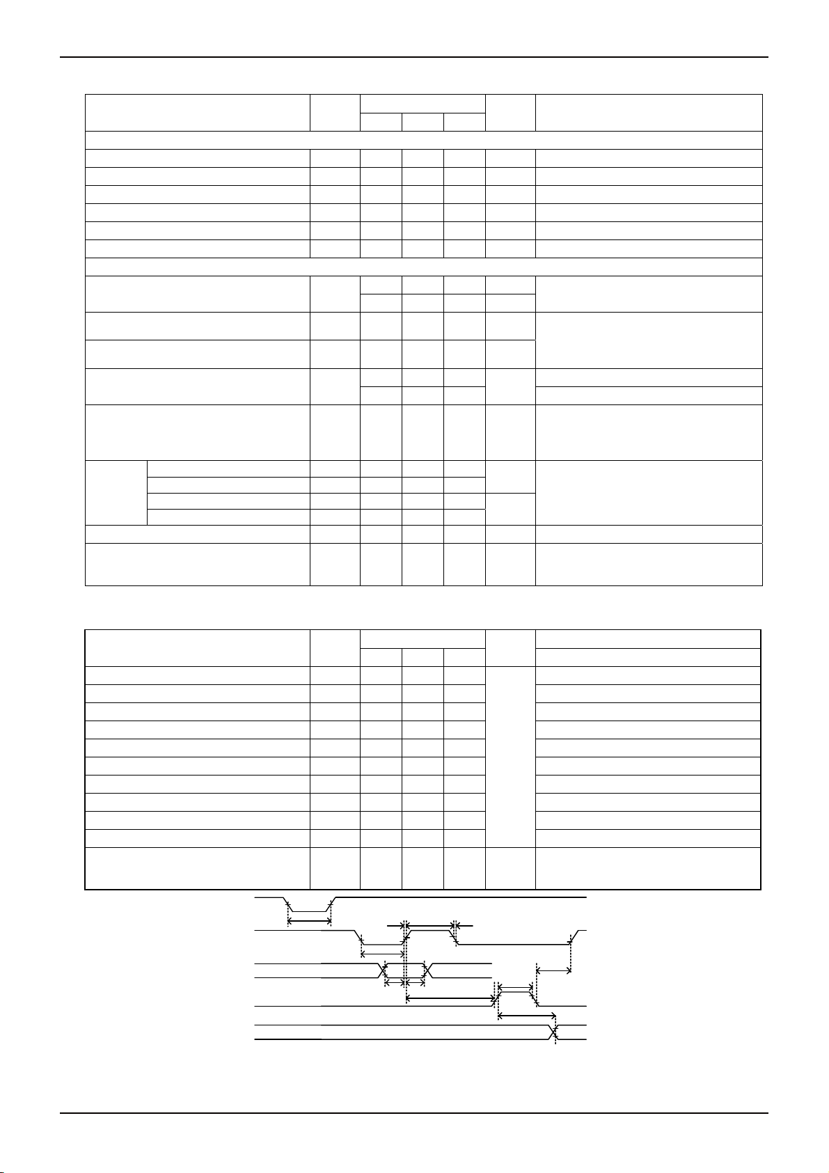
●Timing Characteristics (Unless otherwise specified, VCC=5V, VrefH=5V, VrefL=0V, Ta=25℃)
Parameter Symbol
Limits
MIN. TYP. MAX.
Reset L pulse width tRTL 50 - -
Unit
Judgment level is 80% / 20% of VCC.
Conditions
Clock L pulse width tCKL 50 - - Clock H pulse width tCKH 50 - - Clock rise time tcr - - 50 Clock fall time tcf - - 50 Data setup time tDCH 20 - - -
nS
Data hold time tCHD 40 - - Load setup time tCHL 50 - - Load hold time tLDC 50 - - Load H pulse width tLDH 50 - - -
CL≦100pF, VO:0.5V⇔4.5V .
DA output settling time tLDD - 7 20 μS
Until output value deference from final
value becomes 1/2LSB
RESET
CLK
DI
LD
Output
tRTL
tcr tCKH tcf
tCKL
tDCH tCHD
tCHL
tLDC
tLDH
tLDD
(note) LD signal is level triggered. When LD input is on H level, internal shift-register state is loaded to DAC control latch.
Clock transition during LD=H is inhibited.
www.rohm.com
© 2011 ROHM Co., Ltd. All rights reserved.
2/8
2011.08 - Rev.C
Page 3
BU2508FV,BU2507FV
r
r
r
r
r
Technical Note
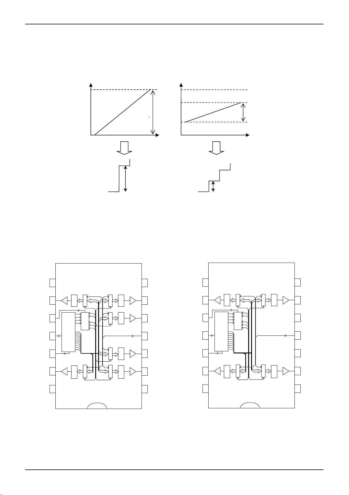
●DAC Variable Output Range Function
With the variable output range function, the upper / lower limits of the output voltage as well as the power supply voltage can be set.
The upper limit value setting terminal VrefH is used as the power supply terminal, while the lower limit value setting terminal
VrefL is used as the GND terminal (1LSB ≒ 5mV). In the example below, VrefH = 3.5V / VrefL = 1.5V. Further adjustments
can be made in order to achieve greater accuracy (1LSB ≒ 2mV).
VOUT
5V
1024
step
ステップ
VOUT
5V
3.5V
1.5V
1024
step
ステップ
VrefH
VrefL
0V
Input Code3FFh
0V
Input Code 3FFh
1LSB≒5.0mV 1LSB≒2.0mV
●Block Diagrams
BU2507FV BU2508FV
891011121314
VCC
L
AO6LDCLKDIAO1GND
D/A
6
D13
12
11
D10
D9
8
14bit
7
6
5
シフトレジスタ
4
Shift registe
3
2
1
D0
10bit R-2R
D/Aコンバータ
DA converte
・・・
アドレス
デコーダ
decoder
Address
10bit Latch
CH1
L
D/A
5
L
D/A
4
L
D/A
3
10bit R-2R
D/Aコンバータ
10bit Latch
DA converte
CH2
Buffer
7654321
VDD
(VrefH)
AO5AO4ResetAO3AO2VSS
バッファ
オペアンプ
amplifier
operation
(VrefL)
891011121314
VCC
L
AO4LDCLKDIAO1GND
D/A
4
D13
12
11
D10
D9
8
14bit
7
6
5
シフトレジスタ
4
Shift register
3
2
1
D0
10bit R-2R
D/Aコンバータ
DA converte
・・・
アドレス
デコーダ
decoder
Address
10bit Latch
CH1
L
D/A
3
10bit R-2R
D/Aコンバータ
10bit Latch
DA converte
CH2
7654321
バッファ
Buffer
オペアンプ
amplifier
operation
VDD
(VrefH)
AO3TEST2ResetTEST1AO2VSS
(VrefL)
www.rohm.com
© 2011 ROHM Co., Ltd. All rights reserved.
3/8
2011.08 - Rev.C
Page 4

BU2508FV,BU2507FV
●Terminal Description
No
Terminal
name
Analog /
Digital
I/O Description of terminal
1 VSS Analog - DA converter lower standard voltage (VrefL) input terminal 6
2 AO2 Analog O 10bit D/A output (CH2) 4
3 AO3(TEST1) Analog O 10bit D/A output (CH3) (BU2508FV : test terminal) 4
4 Reset Digital I All ch analog output L fixed 2
5 AO4(TEST2) Digital I 10bit D/A output (CH4) (BU2508FV : test terminal) 4
6 AO5 (AO3) Analog O 10bit D/A output (CH5) (BU2508FV : 10bit D/A output (CH3)) 4
7 VDD Analog - DA converter upper standard voltage (VrefH) input terminal 5
8 VCC - - Power source terminal -
Technical Note
Equivalent
circuit
9 AO6 (AO4) Analog O 10bit D/A output (CH6) (BU2508FV : 10bit D/A output (CH4)) 4
10 LD Digital I
11 CLK Digital I
12 DI Digital I
When High level is input to LD terminal, the value of 14bit shift
register is loaded to decoder and D/A output register.
Shift clock input terminal. At rise of shift clock, the signal from DI
terminal is input to 14bit shift register.
Serial data input terminal. Serial data whose data length is 14bit
(address 4bit + data 10bit) is input.
13 AO1 Analog O 10bit D/A output (CH1) 4
14 GND - - GND terminal -
*In the case of BU2508FV, be sure to open TEST1 and TEST2 terminals.
●Equivalent Circuits
*1
1
to
inside
2
to
inside
1
1
1
3
*1: 25kΩ at Vcc = 5.0V (changes according to voltage supplied)
www.rohm.com
© 2011 ROHM Co., Ltd. All rights reserved.
from
inside
4
5
・
5
4
・
6
6
4/8
2011.08 - Rev.C
Page 5

BU2508FV,BU2507FV
A
A
A
A
A
A
Technical Note
●Command Sending
1) In the case of BU2507FV
(1) Data format [data : LSB first]
D 13 D 12 D 11 D10 D9 D 8D7D 6 D 5 D 4D3D2D1D0
D/A converter output setting DAT
address select
(2) Data timing diagram
CLK
LD
DACOUT
DDRESS
LSB
D 0 D1 D 2 D 3 D13D 12D 11DI
DDRESS
MSB
DATA
LSB
D 4
DATA
MSB
D3 D2 D1 D0 Address selection
0 0 0 0 Inconsequential
0 0 0 1 Inconsequential
0 0 1 0 AO1 selection
0 0 1 1 AO2 selection
0 1 0 0 Inconsequential
0 1 0 1 AO3 selection
0 1 1 0 AO4 selection
0 1 1 1 Inconsequential
1 0 0 0 AO5 selection
1 0 0 1 AO6 selection
1 0 1 0 Inconsequential
1 0 1 1 Inconsequential
1 1 0 0 Inconsequential
1 1 0 1 Inconsequential
1 1 1 0 Inconsequential
1 1 1 1 Inconsequential
D13 D12 D11 D10 D9 D8 D7 D6 D5 D4 D/A output (VrefH=VDD, VrefL=VSS)
0 0 0 0 0 0 0 0 0 0 VrefL
0 0 0 0 0 0 0 0 0 1 (VrefH-VrefL)/1024×1+VrefL
0 0 0 0 0 0 0 0 1 0 (VrefH-VrefL)/1024×2+VrefL
0 0 0 0 0 0 0 0 1 1 (VrefH-VrefL)/1024×3+VrefL
: : : : : : : : : : :
1 1 1 1 1 1 1 1 1 0 (VrefH-VrefL)/1024×1022+VrefL
1 1 1 1 1 1 1 1 1 1 (VrefH-VrefL)/1024×1023+VrefL
2) In the case of BU2508FV
(1) Data format [Data: LSB first ]
D 13 D 12 D 11 D 10 D 9 D 8D7 D6 D 5 D 4D3 D2 D1 D0
D/A converter output setting DAT
address select
(2) Data timing diagram
DI
CLK
LD
DACOUT
DDRESS
LSB
D 0 D1 D 2 D 3 D 4
DDRESS
MSB
DATA
LSB
DATA
MSB
D13D 12D 11
D3 D2 D1 D0 Address selection
0 0 0 0 Don’t Care
0 0 0 1 Don’t Care
0 0 1 0 AO1 selection
0 0 1 1 AO2 selection
0 1 0 0 Don’t Care
0 1 0 1 Don’t Care
0 1 1 0 Don’t Care
0 1 1 1 Don’t Care
1 0 0 0 AO3 selection
1 0 0 1 AO4 selection
1 0 1 0 Don’t Care
1 0 1 1 Don’t Care
1 1 0 0 Don’t Care
1 1 0 1 Don’t Care
1 1 1 0 Don’t Care
1 1 1 1 Don’t Care
D13 D12 D11 D10 D9 D8 D7 D6 D5 D4 D/A output (VrefH=VDD, VrefL=VSS)
0 0 0 0 0 0 0 0 0 0 VrefL
0 0 0 0 0 0 0 0 0 1 (VrefH-VrefL)/1024×1+VrefL
0 0 0 0 0 0 0 0 1 0 (VrefH-VrefL)/1024×2+VrefL
0 0 0 0 0 0 0 0 1 1 (VrefH-VrefL)/1024×3+VrefL
: : : : : : : : : : :
1 1 1 1 1 1 1 1 1 0 (VrefH-VrefL)/1024×1022+VrefL
1 1 1 1 1 1 1 1 1 1 (VrefH-VrefL)/1024×1023+VrefL
www.rohm.com
© 2011 ROHM Co., Ltd. All rights reserved.
5/8
2011.08 - Rev.C
Page 6

BU2508FV,BU2507FV
●Electrical Characteristics Curves
6
5
4
3
VOUT [V]
2
1
0
0 200 400 600 800 1000 1200
Input Code [decimal]
Fig.1 Output voltage linearity
1.5
1
0.5
0
DNL [LSB]
-0.5
-1
-1.5
0 200 400 600 800 1000 1200
(-30℃)
Input Code [decimal]
6
5
4
3
VOUT [V]
2
1
0
0 200 400 600 800 1000 1200
Input Code [decimal]
Fig.2 Output voltage linearity
(25℃)
1.5
1
0.5
0
DNL [LSB]
-0.5
-1
-1.5
0 200 400 600 800 1000 1200
Input Code [decimal]
Technical Note
6
5
4
3
VOUT [V]
2
1
0
0 200 400 600 800 1000 1200
Input Code [decimal]
Fig.3 Output voltage linearity
(85℃)
1.5
1
0.5
0
DNL [LSB]
-0.5
-1
-1.5
0 200 400 600 800 1000 1200
Input Code [decimal]
Fig.4 Differential linearity error
(-30℃)
1.5
1
0.5
0
INL [LSB]
-0.5
-1
-1.5
0 200 400 600 800 1000 1200
Input Code [decimal]
Fig.7 Integral linearity error
(-30℃)
6
5
4
code=1FFh
3
ICC [mA]
2
1
0
-40 10 60
code=000h
code=3FFh
Temp. [℃]
Fig.5 Differential linearity error
(25℃)
1.5
1
0.5
0
INL [LSB]
-0.5
-1
-1.5
0 200 400 600 800 1000 1200
Input Code [decimal]
Fig.8 Integral linearity error
(25℃)
2.52
2.51
2.5
VOUT [V]
2.49
2.48
-2.5 -1.5 -0.5 0.5 1.5 2.5
Ta= -3 0℃
Ta= 25 ℃
Ta= 85 ℃
IOUT [mA]
Fig.6 Differential linearity error
(85℃)
1.5
1
0.5
0
INL [LSB]
-0.5
-1
-1.5
0 200 400 600 800 1000 1200
Input Code [decimal]
Fig.9 Integral linearity error
(85℃)
1.5
1
0.5
0
DN L [LSB]
-0.5
-1
-1.5
0 200 400 600 800 1000 1200
Input C ode [deci mal
Ta= 85 ℃
Ta= 25 ℃
Ta= -3 0℃
]
Fig.10 Circuit current temperature
characteristic
www.rohm.com
© 2011 ROHM Co., Ltd. All rights reserved.
Fig.11 Output load fluctuation characteristic
(input code : 1FFh)
6/8
Fig.12 Pull-up built in resistance
characteristic
2011.08 - Rev.C
Page 7

BU2508FV,BU2507FV
Technical Note
●Standard Example Application Circuit
V
refH
VCC
AO1
CH1
Vre fL
AO2
AO3
CH2
CH3
Reset
Controller
LD
CLK
DI
GND
AO6
CH6
●Notes for use
(1) The electrical characteristic and data on graphs for this datasheet, are typically evaluated value, and not guaranteed.
(2) We suppose that application circuits are recommendable, but please make sufficient check for characteristics with the
actual application. In case that value of external component for this IC is changed, please check characteristic, not only
static but also transient.
(3) About absolute maximum ratings
If operation condition is over the absolute maximum ratings, supply voltage or other operation range, IC will be broken.
Please don't apply any voltage or temperature over the absolute maximum ratings. If application have possibilities of
become over the absolute maximum ratings, please take safety measures by using fuse and so on. Not to over absolute
maximum ratings of IC.
(4) GND voltage
Please keep GND voltage lowest of any other terminal of this IC. Please confirm other terminal voltages is not lower
than GND.
(5) Thermal design
Please making a thermal design that allows for a sufficient margin in light of the power dissipation in actual operating
condition.
(6) About terminals short and wrong mounting
Please pay full attention to the IC direction and displacement when mounting IC on PCB. If you assemble them by
mistake and electrify it, IC might be destroyed. And it is happen to short among IC terminals or terminals and power
supply, by foreign substance.
(7) About operation in strong electromagnetic field
If you use it in strong electromagnetic field, please evaluate fully as there is a possibility of malfunction.
(8) Place a bypass capacitor as close as possible between each power supply terminal and ground in order to prevent
deterioration of the D/A conversion accuracy due to ripple and noise signals from power supply or GND.
(9) A capacitor should be inserted between the analog output and ground in order to eliminate noise.
A capacitance up to 100pF is recommended (including the capacitance of the wire).
www.rohm.com
© 2011 ROHM Co., Ltd. All rights reserved.
7/8
2011.08 - Rev.C
Page 8

BU2508FV,BU2507FV
●Ordering part number
B U 2 5 0 8 F V - E 2
Technical Note
Part No. Part No.
2507
2508
Package
FV: SSOP-B14
SSOP-B14
<Tape and Reel information>
Quantity
Direction
of feed
6.4 ± 0.3
1.15 ± 0.1
0.2
±
4.4
0.10
14
1
0.65
5.0 ± 0.2
8
0.3Min.
7
0.15 ± 0.1
0.1
0.22 ± 0.1
(Unit : mm)
Packaging and forming specification
E2: Embossed tape and reel
Embossed carrier tapeTape
2500pcs
E2
The direction is the 1pin of product is at the upper left when you hold
()
reel on the left hand and you pull out the tape on the right hand
Direction of feed
Reel
1pin
Order quantity needs to be multiple of the minimum quantity.
∗
www.rohm.com
© 2011 ROHM Co., Ltd. All rights reserved.
8/8
2011.08 - Rev.C
Page 9

Notes
No copying or reproduction of this document, in part or in whole, is permitted without the
consent of ROHM Co.,Ltd.
The content specied herein is subject to change for improvement without notice.
The content specied herein is for the purpose of introducing ROHM's products (hereinafter
"Products"). If you wish to use any such Product, please be sure to refer to the specications,
which can be obtained from ROHM upon request.
Examples of application circuits, circuit constants and any other information contained herein
illustrate the standard usage and operations of the Products. The peripheral conditions must
be taken into account when designing circuits for mass production.
Great care was taken in ensuring the accuracy of the information specied in this document.
However, should you incur any damage arising from any inaccuracy or misprint of such
information, ROHM shall bear no responsibility for such damage.
The technical information specied herein is intended only to show the typical functions of and
examples of application circuits for the Products. ROHM does not grant you, explicitly or
implicitly, any license to use or exercise intellectual property or other rights held by ROHM and
other parties. ROHM shall bear no responsibility whatsoever for any dispute arising from the
use of such technical information.
The Products specied in this document are intended to be used with general-use electronic
equipment or devices (such as audio visual equipment, ofce-automation equipment, communication devices, electronic appliances and amusement devices).
The Products specied in this document are not designed to be radiation tolerant.
While ROHM always makes efforts to enhance the quality and reliability of its Products, a
Product may fail or malfunction for a variety of reasons.
Please be sure to implement in your equipment using the Products safety measures to guard
against the possibility of physical injur y, re or any other damage caused in the event of the
failure of any Product, such as derating, redundancy, re control and fail-safe designs. ROHM
shall bear no responsibility whatsoever for your use of any Product outside of the prescribed
scope or not in accordance with the instruction manual.
The Products are not designed or manufactured to be used with any equipment, device or
system which requires an extremely high level of reliability the failure or malfunction of which
may result in a direct threat to human life or create a risk of human injury (such as a medical
instrument, transportation equipment, aerospace machinery, nuclear-reactor controller, fuelcontroller or other safety device). ROHM shall bear no responsibility in any way for use of any
of the Products for the above special purposes. If a Product is intended to be used for any
such special purpose, please contact a ROHM sales representative before purchasing.
If you intend to export or ship overseas any Product or technology specied herein that may
be controlled under the Foreign Exchange and the Foreign Trade Law, you will be required to
obtain a license or permit under the Law.
Notice
www.rohm.com
© 2011 ROHM Co., Ltd. All rights reserved.
Thank you for your accessing to ROHM product informations.
More detail product informations and catalogs are available, please contact us.
ROHM Customer Support System
http://www.rohm.com/contact/
R1120
A
 Loading...