


1
Standard ICs
8-bit shift register and latch driver
BU2114 / BU2114F
The BU2114 and BU2114F are CMOS ICs with low power consumption, and are equipped with an 8-bit shift register
latch. Data in the shift register can be latched asynchronously. The outputs (O1 to O8) are open drain outputs
(because there is no protection diode, a maximum voltage above V
DD, of up to 7V, can be applied), and one output
can drive 36 mA. A total output of up to 150 mA can be driven (when using static operation).
•
Applications
These are designed for a wide range of applications in microcomputer peripheral circuits, such as in industrial equipment, office telephones, audio visual equipment, and expansion input and output boards.
•
Features
1) The CMOS configuration enables low power con-
sumption.
2) Open drain output.
3) Latch to 8-bit shift register provided, enabling drive
of up to 150mA. (I
SINK = 36mA)
4) Cascade connections possible.
•
Absolute maximum ratings (unless otherwise noted, Ta = 25°C)
Parameter Symbol Limits Unit
Applied voltage
Input voltage
Operating temperature
Storage temperature
Input protection diode current
Power dissipation
V
DD – 0.3 ~ + 7.0 V
V
IN – 0.3 ~ VDD0.3 V
Topr – 25 ~ + 75 °C
Tstg – 55 ~ + 150 °C
ID ± 20 mA
BU2114
Pd
1100
∗1
mW
BU2114F 400
∗2
∗
1 Power dissipation is reduced by 8.8mW for each increase in Ta of 1°C over 25°C.
∗
2 Power dissipation is reduced by 3.2mW for each increase in Ta of 1°C over 25°C.
•
Recommended operating conditions (unless otherwise noted, Ta = 25°C)
䊊Not designed for radiation resistance.
Parameter Symbol Min. Typ. Max. Unit Conditions
Recommend voltage
Input voltage
Output voltage
V
DD 4.5 5.0 5.5 V
V
IN 0 — VDD V SIN, CK, LATCH, EN, RST
V
OUT 0 — VDD V SOUT
2
Standard ICs BU2114 / BU2114F
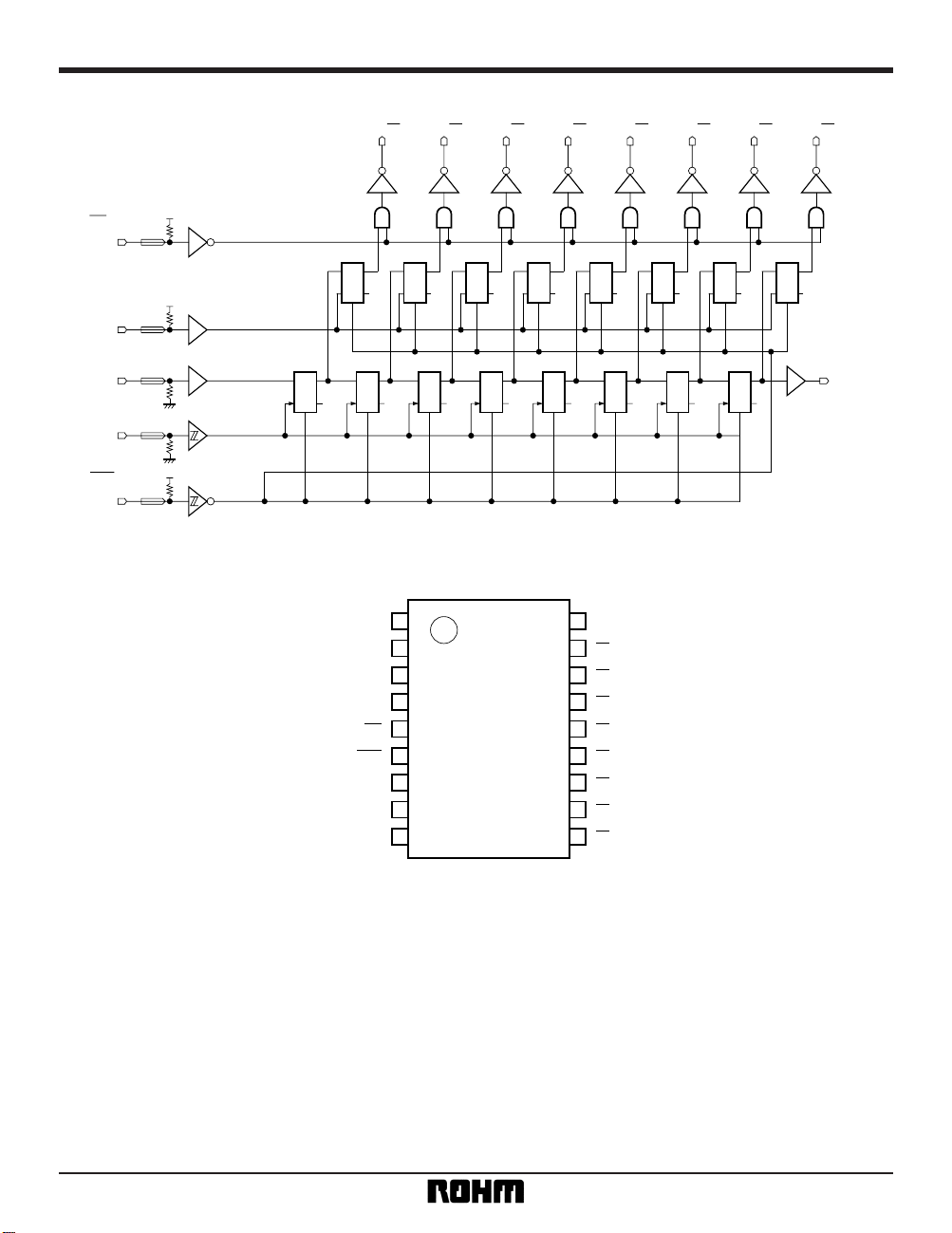
•
Logic circuit diagram
•
Pin assignments
SIN
CK
LATCH
SOUT
EN
RST
GND
GND
GND
01
02
03
04
05
06
07
08
VDD
Fig.1
EN
LATCH
SIN
CK
RST
SOUT
01 02 03 04 05 06 07 08
DQ
R
CQB
DQ
R
CQB
DQ
R
CQB
DQ
R
CQB
DQ
R
CQB
DQ
R
CQB
DQ
R
CQB
DQ
R
CQB
DQ
R
CQB
DQ
R
CQB
DQ
R
CQB
DQ
R
CQB
DQ
R
CQB
DQ
R
CQB
DQ
R
CQB
DQ
R
CQB

3
Standard ICs BU2114 / BU2114F
•
Pin descriptions
Symbol
1 SIN I Serial data input pin
2CK I Shift clock for shift register
3 LATCH I
shift register output changes.
4 SOUT O This is the output for the final-stage shift register.
5EN I
This is the Enable pin for O1 to O8. When this pin is
When the output is "H", however, output QN is "L",
6 RST I Resets the shift register and latch.
7GND —
8GND —
9GND —
10 O8 O Latch output for 8th stage of shift register
11 O7 O Latch output for 7th stage of shift register
12 O6 O Latch output for 6th stage of shift register
13 O5 O Latch output for 5th stage of shift register
14 O4 O Latch output for 4th stage of shift register
15 O3 O Latch output for 3rd stage of shift register
16 O2 O Latch output for 2nd stage of shift register
17 O1 O Latch output for 1st stage of shift register
18 V
DD
—
Setting this pin to "L" holds the latch output. While it is
"H", latch output changes simultaneously when the
"L", the latch output appears as is.
and when the latch output is "L", Qn becomes HighZ
+ VDD power supply
0V power supply
0V power supply
0V power supply
Note 1) O1 to O8 are open drain output, and when the shift register output is "H", the output level goes "L".
Pin No. I / O Function
 Loading...