

Capacitive Sensor Control IC Series
Capacitive Sensor Switch
Control IC
BU21051FS
●Description
BU21051FS are the capacitive sensor controller with 2ch respectively.
The IC has the port interface and easy to replace the point of switch to this controller.
●Features
1) Port output interface
2) Few software control
3) 2ch GPIO outputs
4) 5V power supply voltage available
5) Integrated 10bit AD converter, clock and reset
6) Package SSOP-A16
●Applications
It is possible to use it widely as a switch such as home electric appliance.
●Absolute Maximum Ratings (Ta=25℃)
PARAMETER SYMBOL
MIN MAX
AVD D -0.3 7. 0
Applied voltage
DVDD -0.3 7.0
RATING
UNIT
V
V
-0.3 AVDD + 0.3
Input voltage
Storage temperature
range T
Power dissipation Pd 500 mW
Ambient temperature reduces a permission loss by 5mW per case more than 25 degrees Celsius, 1 degree Celsius
AIN
V
-0.3 DVDD + 0.3
DIN
-55 125 ℃
stg
V
Jan. 2009

●Recommended Operating conditions
PARAMETER SYMBOL
RATING
UNIT
MIN TYP MAX
Applied voltage
AVDD 4.5 5.0 5.5 V
DVDD 4.5 5.0 5.5 V
Operating temperature
T
-40 25 85 ℃
range
opr
●Electrical characteristics(Especially, Topr=25℃ and AVDD=DVDD=0 as long as it doesn't specify it.)
RATING
PARAMETER SYMBOL
UNIT Condition
MIN TYP MAX
DC characteristics
Input“H”voltage V
Input“L”voltage V
Output“H”voltage VOL GND - DVDD x 0.2 V I
Output“L”voltage I
Input leakage current I
DVDD x 0.9 - DVDD + 0.2 V
IHIO
GND – 0.2 - DVDD x 0.1 V
ILIO
-1 - 1 μA
IZ
-1 - 1 μA
OZ
= -2[mA]. Overshoot is excluded.
OH
Output leakage current IST - - 2 μA Shutdown (SDN=“L”)
Standby current I
- 500 - uA
DD
●A/D Converter
RATING
PARAMETER SYMBOL
UNIT Condition
MIN TYP MAX
Resolution - 10 - bit
Analog Input voltage V
Change clock frequency f
Change time f
Zero scale voltage - - GND + 0.07 V
Full scale voltage AVDD - 0.07 - - V
Differential non line accurate DNL - - ±3 LSB
Integrate non line accurate INL - - ±3 LSB
●CR Oscillator characteristic
PARAMETER SYMBOL
Oscillation Frequency f
GND - AVDD V
AIN
0.2 - 1.0 MHz
adck
- 13 - μsec f
tim
adck
RATING
UNIT Condition
MIN TYP MAX
0.9 1.6 2.5 MHz
cr
= 1[MHz]
2/6
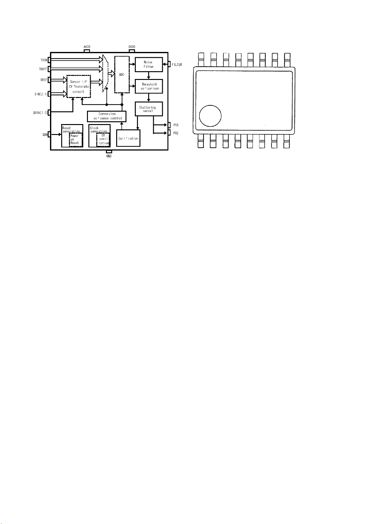
●Block Diagram, Pin configuration
AVDD
TST
THON
THOFF
GAIN[1]
GAIN[0]
FILTER
PO1
DVDD
GND
SREF
SIN1
SDN
PO2
N.C.
SIN2
●Sensor I/F CV Conversion Circuit:
This part selects target sensor and converts its capacitance to a voltage signal. Specifically, alleight
sensors are selected one-by-one and their capacity is compared to a common referencecapacity. Each
difference value is converted to a certain voltage signal.
●AD Conversion
The voltage signal derived from CV conversion is further converted to digital value by this block.
●Conversion Sequence Control
This block controls the process of CV conversion and generates timing of selecting target sensors.
●Noise Filter
The GND level difference between appliance and human body will cause noises to the CV conversion
●Compare threshold
CV converted to sensor data On / Off compared with a threshold, the switch converts the signal.
●Calibration
When the capacitance change do not exceed the threshold for a certain period, this blockstarts-up
calibration process.
●Reset Generation
This is internal reset circuit. Reset is initialized by external SDN signal.
●Clock Generation
Clock from internal RC oscillation circuit is used as system clock.
3/6
●Pin Description
Pin
No Name I/O Function Notes
Supply
referen
Reset level
ce
1 DVDD Power
2 GND Ground
3 SREF AIn
4 SIN1 AIn
Digital part Power supply
Ground
Standard capacitor input
Sensor input1
Digital part Power supply
-
-
-
-
AVD D
AVD D
“Hi-Z” ③
“Hi-Z” ③
5 N.C. - No connect - - - 6 SIN2 AIn
7 THON AIn
8 THOFF AIn
Sensor input 2
Sensor ON threshold
voltage input
Sensor OFF threshold
voltage input
-
- AVDD “Hi-Z” ③
- AVDD “Hi-Z” ③
AVDD “Hi-Z”
9 AVDD Power Analog part Power supply - -
10 TST In Test input Usually tide to “L” DVDD - ①
11 SDN In Shutdown input
“H” : state of operation
“L” : halt condition
DVDD ①
12 PO2 Out Switch output 2 Sensor pin2 On → “L”, Off → “Hi-Z” DVDD “Hi-Z” ②
13 PO1 Out Switch output 1 Sensor pin1 On → “L”, Off → “Hi-Z” DVDD “Hi-Z” ②
14 FILTER In Filter selection
15 GAIN[0] In
Gain level selection
16 GAIN[1] In DVDD ①
“H”: Filter effect: strong
“L”: Filter effect: Weak
GAIN[1:0] = 00 : Strong
GAIN[1:0] = 01 :
GAIN[1:0] = 10 :
GAIN[1:0] = 11 : Week
DVDD ①
DVDD ①
Gain
※*1 Initial State ① When internal organs power-on
reset is effective
② When SDN = “L”
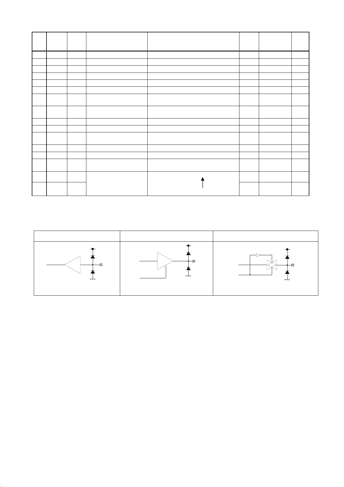
●I/O Circuit
①CMOS input ②CMOS 3state output
③CMOS 3state output with analog switch
I/O
1
※
Pad
③
CIN
PAD
【THON: Button OFF→ON threshold value judge】
【THOFF: Button ON→OFF threshold value judge】
Setting the threshold value of electrostatic Sensor Switches. By applying voltages can be set.
As an example, 1/2VDD applied to the entire range of the sensor output 1 / 2 to set the threshold value.
In fact, the voltage setting resistance to the partial pressure is recommended to us.
【GAIN Selection】
Sensor gain can be set in 4 stages
GAIN[1:0] = 00 (x92)
GAIN[1:0] = 01 (x69)
GAIN[1:0] = 10 (x46)
GAIN[1:0] = 11 (x1)
OEN
PADI
AIN
ASW
PAD
4/6

【Filter selection】
The noise filter effect can be selected If “Strong” is selected, noise will get down, but the reaction time will be longer.
Sensor value
Sensor ON threshold
FILTER=”L”:filter effect →weak
delay time →short
FILTER=”L”:filter effect →strong
delay time →long
Switch detect time
●Setting method
1)Please for the first time in a minimum gain.
2)THOFF = 0V, and, THON 1/2VDD voltage as a guideline for whether or not to switch ON, and gain selection to please the
rough.
Note: ON gain to a minimum, you gain more precision amended to increase the impact too, so please take note.
●Operation Mode
This IC has several modes, called detection mode, calibration mode, and shut-down mode. Each mode
is described as follow
【Detection Mode】
This is normal operation mode of this IC. In this mode, IC detects the sensor capacitance continually.
【Calibration Mode】
Under detection mode when no operation has been detected for sometime, Sensor offset
calibration will be done. And the interval between each calibration is fixed
Detection mode and Calibration mode are switched automatically.
【Shutdown Mode】
When SDN pin is set to “L”, IC will be shut-down and all internal circuits will stop working. IC will work
again when SDN pin is set to “H”.
●Power Supply ON Sequence
This IC has two power input pins AVDD and DVDD. Power ON sequence must be whether set DVDD first
or set the two at one time. Since internal reset circuit is monitoring AVDD, wrong power ON sequence
may cause initialization error.
5/6

●Ordering part number
123
123
123
123
B
U 1 2
5
1 S
F
E20
Part No.
Part No
SSOP-A16
〈Dimension〉
Package
FS :SSOP-A16
〈Tape and Reel information〉
Tape
Quantity
Direction
Embossed carrier tape
2500pcs
E2
(
The direction is the 1pin of product is at the upper left when you hold
reel on the left hand and you pull out the tape on the right hand)
Reel
※When you order , please order in times the amount of package quantity.
Packaging and forming specification
E2:Embossed tape and reel
1234
1Pin
1234
1234
Direction of feed
1234
(Unit:mm)
1st 2009, January
Catalog No.09048EAT05 '09.1 ROHM © Published by LSI Business Promotion Group
6/6

Appendix
No copying or reproduction of this document, in part or in whole, is permitted without the consent of ROHM
CO.,LTD.
The content specified herein is subject to change for improvement without notice.
The content specified herein is for the purpose of introducing ROHM's products (hereinafter "Products"). If you
wish to use any such Product, please be sure to refer to the specifications, which can be obtained from ROHM
upon request.
Examples of application circuits, circuit constants and any other information contained herein illustrate the
standard usage and operations of the Products. The peripheral conditions must be taken into account
when designing circuits for mass production.
Great care was taken in ensuring the accuracy of the information specified in this document. However, should
you incur any damage arising from any inaccuracy or misprint of such information, ROHM shall bear no re-
sponsibility for such damage.
The technical information specified herein is intended only to show the typical functions of and examples
of application circuits for the Products. ROHM does not grant you, explicitly or implicitly, any license to
use or exercise intellectual property or other rights held by ROHM and other parties. ROHM shall bear no re-
sponsibility whatsoever for any dispute arising from the use of such technical information.
The Products specified in this document are intended to be used with general-use electronic equipment
or devices (such as audio visual equipment, office-automation equipment, communication devices, elec-
tronic appliances and amusement devices).
The Products are not designed to be radiation tolerant.
While ROHM always makes efforts to enhance the quality and reliability of its Products, a Product may fail or
malfunction for a variety of reasons.
Please be sure to implement in your equipment using the Products safety measures to guard against the
possibility of physical injury, fire or any other damage caused in the event of the failure of any Product, such as
derating, redundancy, fire control and fail-safe designs. ROHM shall bear no responsibility whatsoever for your
use of any Product outside of the prescribed scope or not in accordance with the instruction manual.
The Products are not designed or manufactured to be used with any equipment, device or system
which requires an extremely high level of reliability the failure or malfunction of which may result in a direct
threat to human life or create a risk of human injury (such as a medical instrument, transportation equipment,
aerospace machinery, nuclear-reactor controller, fuel-controller or other safety device). ROHM shall bear
no responsibility in any way for use of any of the Products for the above special purposes. If a Product is intend-
ed to be used for any such special purpose, please contact a ROHM sales representative before purchasing.
If you intend to export or ship overseas any Product or technology specified herein that may be controlled under
the Foreign Exchange and the Foreign Trade Law, you will be required to obtain a license or permit under the Law.
Notes
Thank you for your accessing to ROHM product informations.
More detail product informations and catalogs are available, please contact your nearest sales office.
ROHM Customer Support System
www.rohm.com
Copyright © 2009 ROHM CO.,LTD.
21 Saiin Mizosaki-cho, Ukyo-ku, Kyoto 615-8585, Japan
THE AMERICAS / EUROPE / ASIA / JAPAN
Contact us : webmaster@ rohm.co. jp
TEL : +81-75-311-2121
FAX : +81-75-315-0172
Appendix-Rev4.0
 Loading...