

Page 1
A
Touch Screen Controller ICs
Resistive Type
Touch Screen Controller ICs
BU21023GUL, BU21023MUV, BU21024FV-M
●Description
Unlike most resistive touch screen controllers, the BU21023/ BU21024 4-wire resistive touch screen controllers enable
dual-touch detection and gesture recognition. These intelligent controllers expose a set of registers to a host processor and
are software configurable. The controllers can detect single point coordinates, dual coordinates, pinch, spread, rotate left
and rotate right gestures, enabling pan and zoom operations in applications that previously had to rely exclusively on
capacitive touch technology. Resistive touch does not require custom panel development which reduces development cost
and results in faster time to market across a family of products.
●Features
1) Enables single touch, dual touch & gesture recognition using standard 4-wire resistive touch panels
2) Adjustable touch detection threshold allows fine tuning of pressure sensitivity for an application
3) Enables measurement of single point touch pressure
4) SPI and I
5) Programmable interrupt polarity
6) 10-bit ADC provides sufficient resolution for finger or stylus inputs
7) Firmware for internal CPU may be downloaded from Host processor or from an EEPROM
8) Includes filtering options to eliminate false coordinates
9) Built in support for intelligent calibration
10) Easy to swap X & Y coordinates or adapt to different touch panel connections
11) Single 3V power supply
12) Available in a range of small package sizes and temperature ranges
13) Ideally suited for large volume automotive, consumer and industrial applications
●Application
・Products with a LCD that can benefit from pan and zoom operations.
・Smart phones, Digital Cameras, Video Cameras, GPS Receivers, Printers,
Copiers, automotive navigation panels, touch kiosks
・Tablet PCs , Notebook computers, LCD displays (with USB interface)
●Line up matrix
2
C like interface for interfacing to host processor
No.11105EAT01
Parameter BU21023GUL BU21023MUV BU21024FV-M
Screen
Maximum detection point
Integrated Filter process
Gesture Detection
Supplied Voltage Range(V)
Temperature Range(℃)
Host I/F
PKG
www.rohm.com
© 2011 ROHM Co., Ltd. All rights reserved.
4-wire resistive
touch screen
2 2 2
Yes Ye s Yes
Yes Ye s Yes
2.7 - 3.6 2.7 - 3.6 2.7 - 3.6
-20 - 85 -20 - 85 -40 - 85
4-wire SPI
2-wire serial
VCSP50L2 VQFN028V5050 SSOP-B28
1/17
4-wire resistive
touch screen
4-wire SPI
2-wire serial
4-wire resistive
touch screens
4-wire SPI
2-wire serial
2011.08 - Rev.
Page 2
A
BU21023GUL,BU21023MUV,BU21024FV-M
●Absolute Maximum Ratings
Parameter Symbol Ratings Unit Condition
Power supply voltage VDD -0.3 ~ 4.5 V
Input voltage VIN VSS-0.3 ~ VDD+0.3 V
*1
BU21023GUL
mW
830
Technical Note
Power dissipation
BU21023MUV 704
Pd
BU21024FV-M 850
*2
mW
*3
mW
Storage temperature range Tstg -50 ~ 125 ℃
*1 Derate by 7.04 mW /℃ centigrade when ambient temperature exceeds 25℃. Measured using Epoxy-Glass PCB measuring 50x58x1.75 mm
*2 Derate by 8.30mW /℃ centigrade when ambient temperature exceeds 25℃. Measured using Epoxy-Glass PCB measuring 50x58x1.75mm
*3 Derate by 8.50mW /℃ centigrade when ambient temperature exceeds 25℃. Measured using Epoxy-Glass PCB measuring 50x58x1.75mm
●Recommended Operating Conditions
Parameter Symbol
Min. Typ. Max.
Ratings
Unit Condition
Power supply voltage VDD 2.70 3.00 3.60 V
Digital core power supply DVDD 1.62 1.80 1.98 V DVDD_EXT=H
BU21023GUL
Operating
temperature range
Note: The BU21023/BU21024 controllers can be operated with a single 3V VDD supply.
It is also possible to supply 1.8V DVDD from an external source if the DVDD_EXT pin is connected to logic high.
BU21023MUV
Topr
BU21024FV-M -40 25 85 ℃
-20 25 85 ℃
●Electrical Characteristics (Ta=25℃, VDD=3.00V)
Parameter Symbol
Min. Typ. Max.
Limits
Unit Condition
Low-level input voltage
High-level input voltage
Low-level output voltage
High-level output voltage
Standby current
Sleep current1
Sleep current2
Operating current
Oscillation frequency
Resolution
Differential non-linearity error
Integral non-linearity error
VIL VSS-0.5 - 0.2×VDD V
VIH 0.8×VDD - VDD+0.5 V
VOL - - VSS+0.4 V
VOH VDD-0.4 - - V
Ist - - 1 µA
Icc1 - 60 100 µA
Icc2 - 10 20 µA
Idd - 4 6 mA
Freq 18 20 22 MHz
Ad 1024×1024 Bit
DNL -3.0 - +3.0 LSB
INL -3.0 - +3.0 LSB
RSTB=L
DVDD_EXT=L
DVDD_EXT=H
No load
www.rohm.com
© 2011 ROHM Co., Ltd. All rights reserved.
2/17
2011.08 - Rev.
Page 3
A
BU21023GUL,BU21023MUV,BU21024FV-M
●HOST-I/F mode (4-wire SPI)
(SCK=SCL_SCK, SI=SDA_SI, CSB=SEL_CSB, SO=SO)
Technical Note
Condition : VDD = 3.0V Ta=25
Parameter Symbol
CSB setup time t1 30 - - ns
SCK "H" level period t2 30 - - ns
SCK "L" level period t3 30 - - ns
SI setup time t4 20 - - ns
SI holding time t5 20 - - ns
CSB holding time t6 20 - - ns
CSB "H" level time t7 50 - - ns
Data output delay time t8 - - 15 ns
SCK frequency t9 - - 15 MHz
Note: SPI interface is selected by tying IFSEL pin to logic low. IFSEL= logic high selects the 2-wire interface
℃
Limits
Min. Typ. Max.
Unit Condition
www.rohm.com
© 2011 ROHM Co., Ltd. All rights reserved.
3/17
2011.08 - Rev.
Page 4
A
BU21023GUL,BU21023MUV,BU21024FV-M
Technical Note
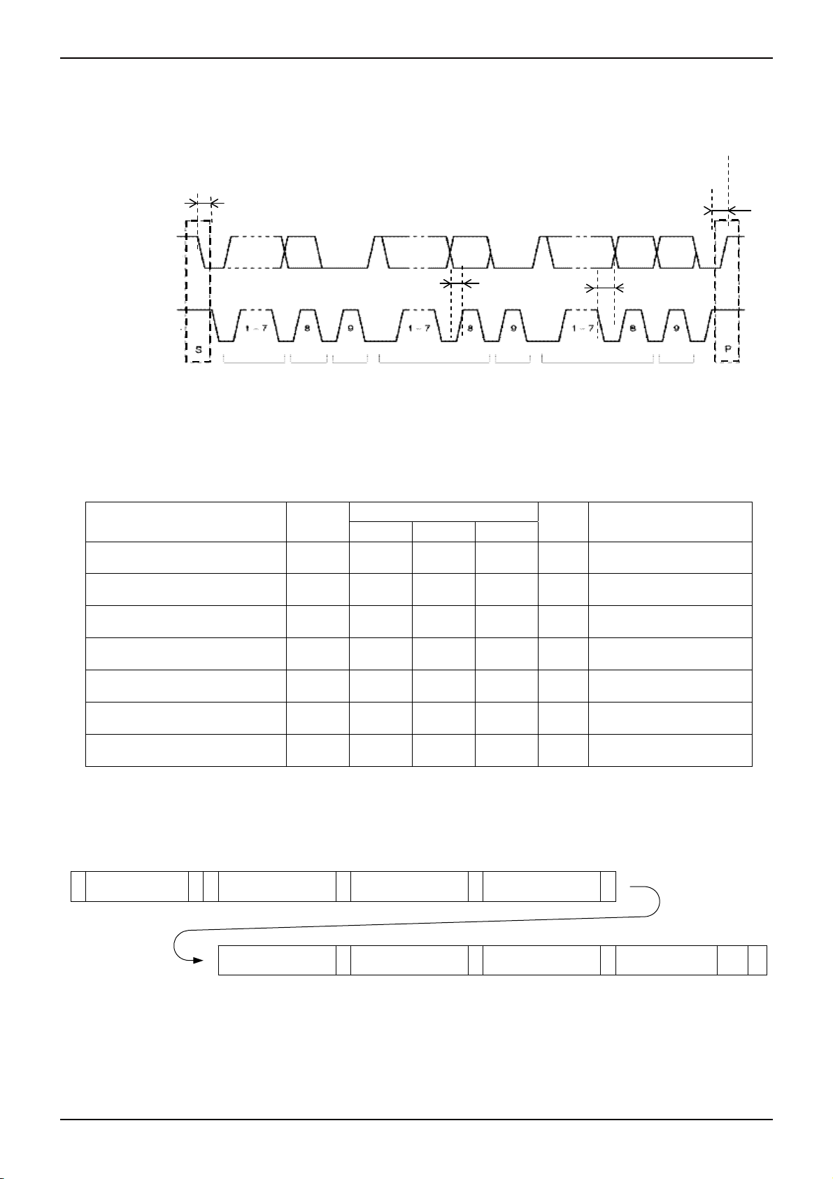
●HOST-I/F mode (2-wire serial)
(SCL=SCL_SCK, SDA=SDA_SI)
The 2-wire serial mode presents an I
conforming to the I
2
C specification. The BU21023MUV/ BU21023GUL / BU21024FV-M devices can co-exist with other I2C
2
C like interface for all practical purposes, but it is not a complete implementation
devices on the same bus. The slave address for 2-wire serial communication is 5Ch or 5Dh. This is determined by the
SEL_CSB pin.
SEL_CSB = “L” : Slave address = 5Ch
SEL_CSB = “H” : Slave address = 5Dh
t
SU;STO
SDA
SDA
SCL
SCL
t
HD;STA
t
SU;DAT
t
HD;DAT
Address ACK
Data Data
ACK
ACK
Parameter Symbol
SCL clock frequency
START condition hold time
SCL “L”
SCL “H”
Data hold time
Data setup time
STOP condition setup time
Min. Typ. Max.
f
0 - 400 kHz
SCL
t
0.6 - - µs
HD:STA
t
1.3 - - µs
LOW
t
0.6 - - µs
HIGH
t
0.1 - - µs
HD:DAT
t
0.1 - - µs
SU:DAT
t
0.6 - - µs
SU:STO
Limits
Unit Condition
・Write protocol
S SLAVE ADDRESS W
7bit = 5Ch or 5Dh 8bit 8bit
A
REGISTER
ADDRESS
A WRITE DATA AP
・Read protocol
S SLAVE ADDRESS W
7bit = 5Ch or 5Dh 8bit 7bit = 5Ch or 5Dh 8bit
from master to slave S = START condition
R = data direction READ (SDA HIGH)
W = data direction WRITE (SDA LOW)
A = acknowledge (SDA LOW)
N = not acknowledge (SDA HIGH)
from slave to master P = STOP condition
A
REGISTER
ADDRESS
A S SLAVE ADDRESS R A READ DATA N P
www.rohm.com
© 2011 ROHM Co., Ltd. All rights reserved.
4/17
2011.08 - Rev.
Page 5
A
BU21023GUL,BU21023MUV,BU21024FV-M
A
A
A
A AAA A
A
A
●EEPROM I/F
BU21023/BU21024 controllers include an EEPROM interface for firmware download.
Device address of EEPROM is set via register 0x51(EEPROM_ADDR).
Timing chart
t
HD;STA
SDA
t
SU;DAT
SCL
Technical Note
t
SU;STO
t
HD;DAT
SCL clock frequency
START hold time
SCL ”L” width
SCL ”H” width
Data hold time
Data setup time
STOP setup time
Protocol
*IC does not support the write command.
*IC supports the following read command.
Start
Address
Parameter Symbol
Read
/Write
ACK
Min. Typ. Max.
f
270 310 350 kHz
SCL
t
0.7 - 0.9 µs
HD:STA
t
1.4 - 1.8 µs
LOW
t
1.4 - 1.8 µs
HIGH
t
0.7 - 0.9 µs
HD:DAT
t
0.7 - 0.9 µs
SU:DAT
t
0.7 - 0.9 µs
SU:STO
Data Data
Limits
ACK
Unit Condition
ACK
S
SLAVE
DDRESS
W
1st WORD
DDRESS
DATA(n-3)
2nd WORD
DDRESS
DATA(n-2)
DATA(0)
DATA(n-1)
DATA(n) P
N
Stop
www.rohm.com
© 2011 ROHM Co., Ltd. All rights reserved.
5/17
2011.08 - Rev.
Page 6

A
BU21023GUL,BU21023MUV,BU21024FV-M
●Background Information
A resistive touch panel is made up of a multilayer sandwich of resistive films and protective coatings all sitting on top of an
LCD display. Resistive touch panels work by direct contact of a stylus or a finger flexing a pair of resistive films, hence any
blunt pointing instrument or a gloved finger may be used.
Touch panel resolution
The resolution of a touch panel is typically measured in dots per inch (dpi) and is a function of the physical size of the touch
panel and the ADC used in the conversion circuitry. For example, a 3”x5” panel used with the BU21023/BU21024 devices
can provide a theoretical resolution of 1024 /5 = 204 dpi. In the case of resistive touch panels, the direct contact nature of its
operation and finger thickness often impose an upper limit on the effective system resolution that may be achieved,
regardless of the resolution of the ADC itself.
●Functional Description
The BU21023/BU21024 devices connect to a standard 4-wire resistive touch screen on one side and to a host processor on
the other side. The BU21024 includes four additional sense terminals allowing it to be used with either 4-wire or 8-wire
resistive touch screens. The BU21023/BU21024 include the analog and digital circuitry to process and provide dual touch
coordinate data and pinch, spread, rotate-right and rotate-left gesture information to the host CPU.
The BU21023/BU21024 devices include an internal CPU and provide a high degree of programmability by exposing a set of
registers that can be accessed by a host CPU through SPI or I
SPI or I
via registers. When an interrupt occurs, for example, due to touch detection, the host processor is required to read an
interrupt status register to determine the cause of the interrupt and take appropriate action.
The program memory of the internal CPU may be initialized via the host interface or via an external EEPROM. This is
selected by a register setting.
The BU21023/BU21024 devices support two sensing modes; continuous and interval sensing modes, that are register
selectable. In the continuous sensing mode, the embedded CPU reads Z, X & Y coordinates continuously when a touch is
detected. The interval sensing mode allows a delay to be inserted between each cycle. The continuous sensing mode is
used more often though the interval sensing mode minimizes power consumption. The continuous sensing mode typically
completes a sampling cycle consisting of Z, X & Y measurements in approximately 2.3 mS.
The BU21023/BU21024 devices enable optimization of touch detection threshold for a given panel. They also include
several sophisticated calibration algorithms.
This document includes a description of the registers followed by flow charts that describe specific steps that a host
processor must follow. Often, a flow chart requires other flow charts to explain the steps in finer detail.
The document also includes information on touch screen parameters that one should to look for while selecting resistive
touch panels for multi-touch.
2
C like interface is selected, The BU21023/BU21024 devices include an INT pin whose polarity can be programmed
2
C like serial interfaces. The IFSEL pin determines whether
Technical Note
www.rohm.com
© 2011 ROHM Co., Ltd. All rights reserved.
6/17
2011.08 - Rev.
Page 7

A
BU21023GUL,BU21023MUV,BU21024FV-M
r
A
A
y
r
r
K
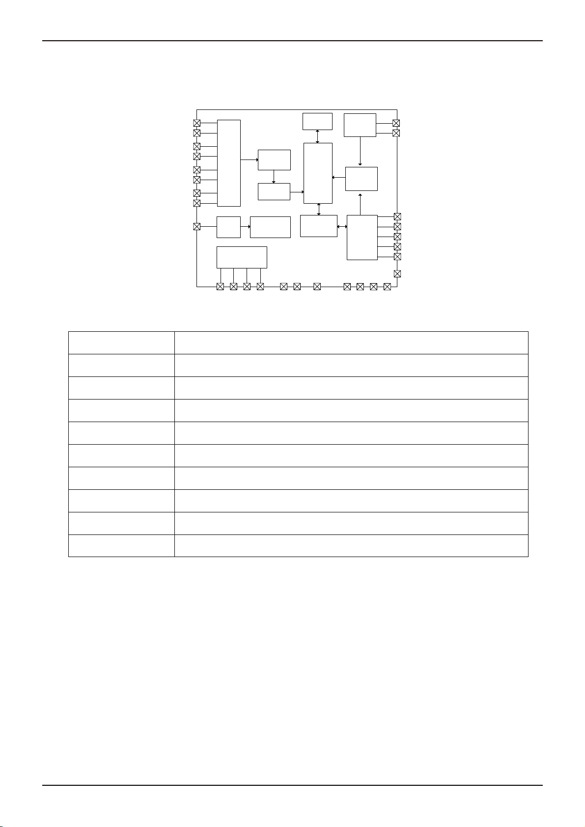
●Block Diagram / Description of each block
【BU21023GUL / BU21023MUV】
XP
Work
Memory
EEPROM
I/F
Technical Note
ECL
EDA
XN
YP
YN
CLK_EXT
Panel
I/F
OSC
PVDD
Regulato
VDD
Generato
DVDD
(10bit)
Filter
Clock
DVDD_EXT
DC
CPU
(8bit)
Registe
VSS
VDD
RSTB
Program
Memor
Host
I/F
T2
T1
SEL_CSB
SCL_SC
SDA_SI
SO
INT
IFSEL
T3
T4
Screen I/F 4-wire resistive touch screen interface
ADC 10bit A/D converter
OSC Internal 20MHz oscillator block with optional external clock input
Regulator
Internal regulator provides 1.8V DVDD supply. DVDD can also be supplied from an
external source if DVDD_EXT pin is tied high.
Clock Generator System clock and timing generation (10MHz CPU clock)
CPU Core For dual touch processing, programmability and host interface
Work memory Data memory for CPU
Program Memory
EEPROM I/F
Program memory for CPU. Code can be downloaded by host processor or from an
external EEPROM
To connect to external EEPROM if downloading program memory from EEPROM. Use
of external EEPROM is optional.
Host I/F 4-wire SPI or 2-wire I2C like interface provides access to registers
www.rohm.com
© 2011 ROHM Co., Ltd. All rights reserved.
7/17
2011.08 - Rev.
Page 8
A
BU21023GUL,BU21023MUV,BU21024FV-M
【BU21024FV-M】
XP
XN
YP
YN
XPM
XNM
YPM
YNM
Panel
I/F
(10bit)
CLK_EXT
Osc
Clock
generator
Regulator
PVDD
AVDD
DVDD
DVDD_EXT
Screen I/F 4-wire or 8-wire resistive touch screen interface
ADC
Filter
Technical Note
Work
memory
CPU
(8bit)
register
VSS
VDD
EEPROM
I/F
Program
memory
Host
I/F
T1
RSTB
T2
ECL
EDA
SEL_CSB
SCL_SCK
SDA_SI
SO
INT
IFSEL
T3
T4
ADC 10bit A/D converter
OSC Internal 20MHz oscillator block with optional external clock input
Regulator
Internal regulator provides 1.8V DVDD supply. DVDD can also be supplied from an
external source if DVDD_EXT pin is tied high.
Clock Generator System clock and timing generation (10MHz CPU clock)
CPU Core For dual touch processing, programmability and host interface
Work memory Data memory for CPU
Program Memory
EEPROM I/F
Program memory for CPU. Code can be downloaded by host processor or from an
external EEPROM
To connect to external EEPROM if downloading program memory from EEPROM. Use
of external EEPROM is optional.
Host I/F 4-wire SPI or 2-wire I2C like interface provides access to registers
www.rohm.com
© 2011 ROHM Co., Ltd. All rights reserved.
8/17
2011.08 - Rev.
Page 9

A
BU21023GUL,BU21023MUV,BU21024FV-M
Technical Note
●Pin Description
【BU21023GUL】
No. Pin name I/O Function Fig.
D1 YN I/O Panel interface E
C1 XN I/O Panel interface E
C2 YP I/O Panel interface E
B1 XP I/O Panel interface E
A1 T4 I/O Test pin E
A2 PVDD O Regulator output (for supply panel voltage) -
B3 AVDD O Regulator output (for supply analog block) -
A3 DVDD I/O
Regulator output (for supply digital block) or supply digital voltage
(DVDD_EXT="H")
B4 DVDD_EXT I Digital voltage enable (H=Hi-z , L=DVDD Enable) E
A4 VDD - Supply voltage -
A5 VSS - Ground -
C3 RSTB I H/W reset E
B5 CLK_EXT I Supply external clock for debug A
C4 T1 I Test pin A
C5 T2 I Test pin A
D4 T3 I Test pin A
D5 IFSEL I Intereface select pin (L=SPI, H=2wire serial) A
D3 SO O SPI Serila data output 2wire - F
E5 INT O Interrupt output C
D2 SEL_CSB I SPI Chip select 2wire Slave address select C
E4 SDA_SI I/O SPI Serial data input 2wire Serial data in-out C
E3 SCL_SCK I SPI Serial clock input 2wire Serial clock input C
E2 EDA I/O EEPROM SDA C
E1 ECL O EEPROM SCL C
1. Please use 1.0uF capacitors between AVDD and DVDD to GND, and leave PVDD terminal open.
2. If DVDD_EXT=”H “, the DVDD pin can be connected to an external 1.8V power source.
3. Please pull up the ECL, EDA, and INT pins using 10k ohm resistors as shown in the application diagram at the end of this document.
ECL and EDA pins may be directly connected to GND if an external EEPROM is not being used. Please connect a 0.1uF capacitor between T4 and GND.
T1, T2 & T3 pins should be connected to GND.
4. When using the 2 wire serial interface, please pull up the SCL_SCK, SDA_SI pins via 10k ohms and leave SO unconnected.
5. Please note that the values of resistors and capacitors mentioned here are only recommended values.
6. RSTB should be held low until supply voltage VDD has ramped up and has reached a stable level.
7. The polarity of INT pin is programmable via register 0x30
8. Connect CLK_EXT to GND for normal use
T4 PVDD DVDD VDD VSS
A
XP AVDD DVDD_EXT CLK_EXT
B
XN YP RSTB T1 T2
C
YN SEL_CSB SO T3 IFSEL
D
ECL EDA SCL_SCK SDA_SI INT
E
ECL EDA SCL_SCK SDA_SI IN T
E
YN SEL_CSB SO T3 IFSEL
D
XN YP RSTB T1 T2
C
XP AVDD DVDD_EXT CLK_EXT
B
T4 PVDD DVDD VDD VSS
A
-
12345
TOP VIEW (BALL SIDE DOWN)
www.rohm.com
© 2011 ROHM Co., Ltd. All rights reserved.
9/17
12345
BOTTOM VIEW (BALL SIDE UP)
2011.08 - Rev.
Page 10

A
BU21023GUL,BU21023MUV,BU21024FV-M
Technical Note
【BU21023MUV】
No. Pin name I/O Function fig
1 NC - - -
2 NC - - -
3 NC - - -
4 YN I/O Panel interface E
5 XN I/O Panel interface E
6 YP I/O Panel interface E
7 XP I/O Panel interface E
8 T4 I/O Test pin E
9 PVDD O Regulator output (for supply panel voltage) -
10 AVDD O Regulator output (for supply analog block) -
11 DVDD I/O
Regulator output (for supply digital block) or supply digital voltage
(DVDD_EXT="H")
12 DVDD_EXT I Digital voltage enable (H=Hi-Z , L=DVDD enable) E
13 VDD - Supply voltage -
14 VSS - Ground -
15 RSTB I H/W reset E
16 CLK_EXT I Supply external clock for debug A
17 T1 I Test pin A
18 T2 I Test pin A
19 T3 I Test pin A
20 IFSEL I Intereface select pin (L=SPI, H=2wire serial) A
21 SO O SPI Serila data output 2wire - F
22 INT O Interrupt output C
23 SEL_CSB I SPI Chip select 2wire Slave address select C
24 SDA_SI I/O SPI Serial data input 2wire Serial data in-out C
25 SCL_SCK I SPI Serial clock input 2wire Serial clock input C
26 EDA I/O EEPROM SDA C
27 ECL O EEPROM SCL C
28 NC - - -
1. Please use 1.0uF capacitors between AVDD and DVDD to GND, and leave PVDD terminal open.
2. If DVDD_EXT=”H “, the DVDD pin can be connected to an external 1.8V power source.
3. Please pull up the ECL, EDA, and INT pins using 10k ohm resistors as shown in the application diagram at the end of this document.
ECL and EDA pins may be directly connected to GND if an external EEPROM is not being used. Please connect a 0.1uF capacitor between
T4 and GND. T1, T2 & T3 pins should be connected to GND.
4. When using the 2 wire serial interface, please pull up the SCL_SCK, SDA_SI pins via 10k ohms and leave SO unconnected.
5. Please note that the values of resistors and capacitors mentioned here are only recommended values.
6. RSTB should be held low until supply voltage VDD has ramped up and has reached a stable level.
7. The polarity of INT pin is programmable via register 0x30
8. Connect CLK_EXT to GND for normal use
1
3
5T16
7
8
T4
9
PVDD
10
AVDD
11
DVDD
12
DVDD_EXT
13
VDD
14
VSS
SEL_CSB
SDA_SI
SCL_SCK
EDA
ECL
2
21 SO
20 I FSEL
19 T3
18 T2
17 T1
16 CLK_EXT
15 RSTB
22INT
23
24
25
26
27
NC
28
14 VSS
VDD
13
DVDD_EXT
12
DVDD
11
AVDD
10
PVDD
9
T4
8
ECL
EDA
SCL_SCK
SDA_SI
SEL_CSB
INT
28
NC
27
26
25
24
23
22
4
-
www.rohm.com
© 2011 ROHM Co., Ltd. All rights reserved.
1NC
2NC
3NC
4YN
5XN
TOP VIEW (LEAD SIDE DOWN)
7XP
6YP
10/17
21 NC
20 NC
19 NC
18 YN
17 XN
16 YP
T3
SO
BOTTOM VIEW (LEAD SIDE UP)
T2
IFSEL
CLK_EXT
15 XP
RSTB
2011.08 - Rev.
Page 11

A
BU21023GUL,BU21023MUV,BU21024FV-M
Technical Note
【BU21024FV-M】
No. Pin name I/O Function fig
1 EDA I/O EEPROM SDA C
2 ECL O EEPROM SCL C
3 YNM I/O Panel interface (Test input) E
4 XNM I/O Panel interface (Test input) E
5 YPM I/O Panel interface (Test input) E
6 XPM I/O Panel interface (Test input) E
7 YN I/O Panel interface E
8 XN I/O Panel interface E
9 YP I/O Panel interface E
10 XP I/O Panel interface E
11 T4 I/O Test pin E
12 PVDD O Regulator output (for supply panel voltage) -
13 AVDD O Regulator output (for supply analog block) -
14 DVDD I/O
Regulator output (for supply digital block) or supply digital voltage
(DVDD_EXT="H")
15 DVDD_EXT I Digital voltage enable (H=Hi-Z , L=DVDD enable) E
16 VDD - Supply voltage -
17 VSS - Ground -
18 RSTB I H/W reset E
19 CLK_EXT I Supply external clock for debug A
20 T1 I Test pin A
21 T2 I Test pin A
22 T3 I Test pin A
23 IFSEL I Intereface select pin (L=SPI, H=2wire serial) A
24 SO O SPI Serila data output 2wire - F
25 INT O Interrupt output C
26 SEL_CSB I SPI Chip select 2wire Slave address select C
27 SDA_SI I/O SPI Serial data input 2wire Serial data in-out C
28 SCL_SCK I SPI Serial clock input 2wire Serial clock input C
1. Please use 1.0uF capacitors between AVDD and DVDD to GND, and leave PVDD terminal open.
2. If DVDD_EXT=”H “, the DVDD pin can be connected to an external 1.8V power source.
3. Please pull up the ECL, EDA, and INT pins using 10k ohm resistors as shown in the application diagram at the end of this document.
ECL and EDA pins may be directly connected to GND if an external EEPROM is not being used. Please connect a 0.1uF capacitor between
T4 and GND. T1, T2 & T3 pins should be connected to GND.
4. When using the 2 wire serial interface, please pull up the SCL_SCK, SDA_SI pins via 10k ohms and leave SO unconnected.
5. Please note that the values of resistors and capacitors mentioned here are only recommended values.
6. RSTB should be held low until supply voltage VDD has ramped up and has reached a stable level.
7. The polarity of INT pin is programmable via register 0x30
8. Connect CLK_EXT to GND for normal use
9. Please leave the XPM, XNM, YPM, YNM terminals open if using a 4-wire touch screen. These pins should be connected to the reference leads of an
8-wire touch screen if one is being used.
SCL_ SCK
SEL_ CSB
SDA _SI
28
27
26
SO
IFSEL
INT
25
24
23
T3
T2
T1
22
21
20
RSTB
VSS
VDD
CLK_EXT
19
18
17
DVDD_EXTDVDD
16
15
-
www.rohm.com
© 2011 ROHM Co., Ltd. All rights reserved.
TOP VIEW
1
2
3
4
5
6
7
8
9
10
11
12
13
14
ECL
EDA
YNM
YPM
XNM
YN
XPM
YP
XN
T4
XP
PVDD
AVDD
TOP VIEW
11/17
2011.08 - Rev.
Page 12
A
BU21023GUL,BU21023MUV,BU21024FV-M
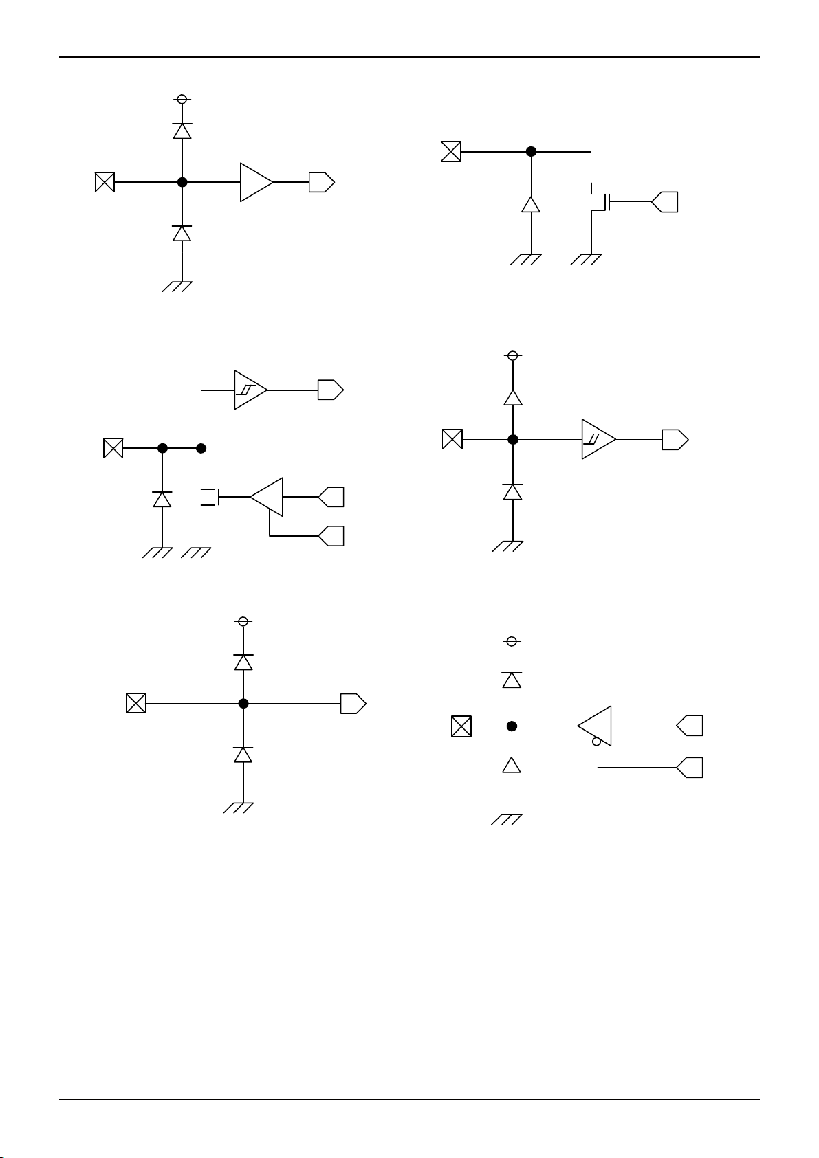
PAD
Technical Note
PAD
Fig. A
Fig. B
PAD
PAD
Fig. C
Fig. D
PAD
CIN
PAD
●Fig. BU21023GUL / BU21023MUV / BU21024FV-M I/O equivalent circuit
www.rohm.com
© 2011 ROHM Co., Ltd. All rights reserved.
Fig. E Fig. F
12/17
2011.08 - Rev.
Page 13
A
BU21023GUL,BU21023MUV,BU21024FV-M
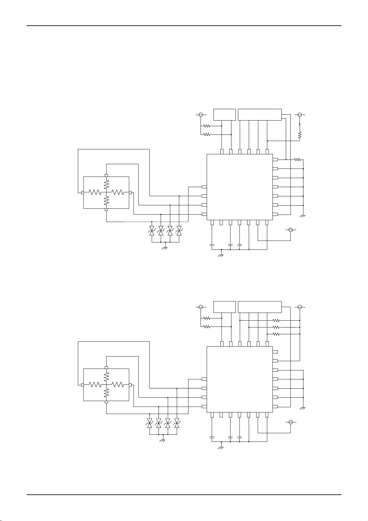
●Application Circuit
【BU21023GUL/BU21023MUV】
BU21023GUL/MUV support 2 host interfaces (4-wire SPI and 2-wire serial bus).
The figures below are shown application circuit when each interface is used.
(Although BU21023GUL is CSP package, it is shown in similar figure for comparing.)
*Please connect the terminal of ECL/EDA with VSS, when firmware is download form HOST.
*Please insert TVS diode each sensor line from the perspective that enhances resistance to ESD.
*In 4-wire SPI using case, pull up INT terminal to VDD or host IO voltage (max4.5V).
If no using, connect to GND.
VDD
EEPROM
10kohm
10kohm
EDA
ECL
panel
YN
XN
YP
XP
SCL_SCK
BU21023
SDA_SI
Host
SEL_CSB
Technical Note
VDD
10kohm
INT
(10kohm)
SO
IFSEL
T3
T2
T1
EXT_CLK
RSTB
TVS diode
T4
AVDD
PVDD
0.1uF 1.0uF 1.0uF
DVDD
Example 1 : BU21023GUL/MUV application circuit(4-wireSPI)
In 2-wire serial interface using case,
please pull up INT, SCL_SCK, SDA_SI terminal to VDD or host IO voltage(max4.5V).
VDD
EEPROM
10kohm
10kohm
EDA
ECL
panel
YN
XN
YP
XP
SCL_SCK
BU21023
VSS
VDD
DVDD_EXT
VDD
Host
10kohm
10kohm
10kohm
SDA_SI
SEL_CSB
INT
SO
IFSEL
T3
T2
T1
EXT_CLK
RSTB
VDD
www.rohm.com
© 2011 ROHM Co., Ltd. All rights reserved.
TVS diode
T4
AVDD
PVDD
0.1uF 1.0uF 1.0uF
DVDD
DVDD_EXT
VSS
VDD
Example 2 : BU21023GUL/MUV application circuit(2-wire Serial bus)
13/17
VDD
2011.08 - Rev.
Page 14

A
BU21023GUL,BU21023MUV,BU21024FV-M
【BU21024FV-M】
BU21024FV-M support 2 host interfaces (4-wire SPI and 2-wire serial bus).
The figures below are shown Application Circuit when each interface is used.
(Although BU21023GUL is CSP package, it is shown in similar figure for comparing.)
*Please connect the terminal of ECL/EDA with VSS, when Firmware is download form HOST.
*Please insert TVS diode each sensor line from the perspective that enhances resistance to ESD.
*In 4-wire SPI using case, pull up INT terminal to VDD or host IO voltage(max4.5V).
If no using, connect to GND.
VDD
VDD
Technical Note
VDD
panel
TVS diode
EEPROM
10kohm 10kohm
0.1uF
1.0uF
1.0uF
EDA
1
ECL
2
YNM
3
XNM
4
YPM
5
XPM
6
YN
7
8
9
10
11
12
13
14
BU21024FV-M
XN
YP
XP
T4
PVDD
AVDD
SCL_SCK
SEL_CSB
CLK_EX T
DVDD_EXTDVDD
SDA_SI
IFSEL
RSTB
VSS
VDD
28
27
26
25
INT
SO
24
23
T3
22
T2
21
T1
20
19
18
17
16
15
10kohm
Host
(10kohm)
VDD
Example 3 : BU21024FV-M Application Circuit(4-wireSPI)
VDD
VDD
VDD
10kohm 10kohm
panel
TVS diode
EEPROM
0.1uF
1.0uF
1.0uF
EDA
1
ECL
2
YNM
3
XNM
4
YPM
5
XPM
6
YN
7
8
9
10
11
12
13
14
BU21024FV-M
XN
YP
XP
T4
PVDD
AVDD
SCL_SCK
SEL_CSB
CLK_E XT
DVDD_EXTDVDD
Example 4 : BU21024FV-M Application Circuit(2-wire Serial bus)
SDA_SI
IFSEL
RSTB
VSS
VDD
10kohm
28
27
26
25
INT
SO
24
23
T3
22
T2
21
T1
20
19
18
17
VDD
16
15
Host
VDD
www.rohm.com
© 2011 ROHM Co., Ltd. All rights reserved.
14/17
2011.08 - Rev.
Page 15

A
BU21023GUL,BU21023MUV,BU21024FV-M
Technical Note
BU21024FV-M has the other pins for debug except for 4-wire resistive touch screen interface (XP, YP, XN, YN).
When debug, there are 4 monitor pins corresponding to four past terminals.
(In 4-wire, supply and detect voltage of screen on 4 pins. When debug, if this function is enable,
it is possible to supply voltage on past 4pins and detect voltage on 4 pins with **M separately. )
To remove the noise of Screen itself, the filter is composed of discrete circuit.
It is possible to ease the decrease of screen voltage's dynamic range, which is caused by wiring resistance on the PCB.
Note: These debug terminals are only for debug. So, please don’t use them in normal application using.
VDD
VDD
VDD
10kohm 10kohm
panel
TVS diode
EEPROM
10 ohm
10 ohm
10 ohm
EDA
1
ECL
2
YNM
3
1nF
XNM
4
1nF
1nF
1nF
0.1uF
1.0uF
1.0uF
YPM
5
XPM
6
YN
7
8
9
10
11
12
13
14
BU21024FV-M
XN
YP
XP
T4
PVDD
AVDD
SCL_SCK
SEL_CSB
CLK_EX T
DVDD_EXTDVDD
SDA_SI
IFSEL
RSTB
VSS
VDD
28
27
26
25
INT
SO
24
23
T3
22
T2
21
T1
20
19
18
17
16
15
Example 5 : BU21024FV-M Application Circuit(4-wireSPI with RC filter)
VDD
VDD
10kohm
Host
(10kohm)
VDD
VDD
panel
TVS diode
EEPROM
10kohm 10kohm
10 ohm
10 ohm
10 ohm
1nF
10 ohm
1nF
EDA
1
ECL
2
YNM
3
1nF
XNM
4
1nF
0.1uF
1.0uF
1.0uF
YPM
5
XPM
6
YN
7
8
9
10
11
12
13
14
BU21024FV-M
XN
YP
XP
T4
PVDD
AVDD
SCL_SCK
SEL_CSB
CLK_EX T
DVDD_EXTDVDD
SDA_SI
IFSEL
RSTB
VSS
VDD
28
27
26
25
INT
SO
24
23
T3
22
T2
21
T1
20
19
18
17
16
15
10kohm
VDD
Example 6 : BU21024FV-M Application Circuit(2-wire Serial bus with RC filter)
Host
VDD
www.rohm.com
© 2011 ROHM Co., Ltd. All rights reserved.
15/17
2011.08 - Rev.
Page 16

A
BU21023GUL,BU21023MUV,BU21024FV-M
●Notes for use
(1) Absolute Maximum Ratings
An excess in the absolute maximum ratings, such as supply voltage, temperature range of operating conditions, etc.,
can break down devices thus making impossible to identify breaking mode such as a short circuit or an open circuit. If
any special mode exceeding the absolute maximum ratings is assumed, consideration should be given to take physical
safety measures including the use of fuses, etc.
(2) Operating conditions
These conditions represent a range within which characteristics can be provided approximately as expected. The
electrical characteristics are guaranteed under the conditions of each parameter.
(3) Reverse connection of power supply connector
The reverse connection of power supply connector can break down ICs. Take protective measures against
the breakdown due to the reverse connection, such as mounting an external diode between the power supply
and the IC's power supply terminal.
(4) Power supply line
Design PCB pattern to provide low impedance for the wiring between the power supply and the GND lines. In this regard,
for the digital block power supply and the analog block power supply, even though these power supplies has the same
level of potential, separate the power supply pattern for the digital block from that for the analog block, thus suppressing
the diffraction of digital noises to the analog block power supply resulting from impedance common to the wiring
patterns. For the GND line, give consideration to design the patterns in a similar manner. Furthermore, for all power
supply terminals to ICs, mount a capacitor between the power supply and the GND terminal. At the same time, in order
to use an electrolytic capacitor, thoroughly check to be sure the characteristics of the capacitor to be used present no
problem including the occurrence of capacity dropout at a low temperature, thus determining the constant.
(5) GND voltage
Make setting of the potential of the GND terminal so that it will be maintained at the minimum in any operating state.
Furthermore, check to be sure no terminals are at a potential lower than the GND voltage including an actual electric
transient.
(6) Short circuit between terminals and erroneous mounting
In order to mount ICs on a set PCB, pay thorough attention to the direction and offset of the ICs. Erroneous mounting
can break down the ICs. Furthermore, if a short circuit occurs due to foreign matters entering between terminals or
between the terminal and the power supply or the GND terminal, the ICs can break down.
(7) Operation in strong electromagnetic field
Be noted that using ICs in the strong electromagnetic field can malfunction them.
(8) Inspection with set PCB
On the inspection with the set PCB, if a capacitor is connected to a low-impedance IC terminal, the IC can suffer stress.
Therefore, be sure to discharge from the set PCB by each process. Furthermore, in order to mount or dismount the set
PCB to/from the jig for the inspection process, be sure to turn OFF the power supply and then mount the set PCB to the
jig. After the completion of the inspection, be sure to turn OFF the power supply and then dismount it from the jig. In
addition, for protection against static electricity, establish a ground for the assembly process and pay thorough attention
to the transportation and the storage of the set PCB.
(9) Input terminals
In terms of the construction of IC, parasitic elements are inevitably formed in relation to potential. The operation of the
parasitic element can cause interference with circuit operation, thus resulting in a malfunction and then breakdown of
the input terminal. Therefore, pay thorough attention not to handle the input terminals, such as to apply to the input
terminals a voltage lower than the GND respectively, so that any parasitic element will operate. Furthermore, do not
apply a voltage to the input terminals when no power supply voltage is applied to the IC. In addition, even if the power
supply voltage is applied, apply to the input terminals a voltage lower than the power supply voltage or within the
guaranteed value of electrical characteristics.
(10) Ground wiring pattern
If small-signal GND and large-current GND are provided, It will be recommended to separate the large-current GND
pattern from the small-signal GND pattern and establish a single ground at the reference point of the set PCB so that
resistance to the wiring pattern and voltage fluctuations due to a large current will cause no fluctuations in voltages of
the small-signal GND. Pay attention not to cause fluctuations in the GND wiring pattern of external parts as well.
(11) External capacitor
In order to use a ceramic capacitor as the external capacitor, determine the constant with consideration given to a
degradation in the nominal capacitance due to DC bias and changes in the capacitance due to temperature, etc.
(12) Rush current
The IC with some power supplies has a capable of rush current due to procedure and delay at power-on. Pay attention
to the capacitance of the coupling condensers and the wiring pattern width and routing of the power supply and the GND
lines.
(13) Others
In case of use this LSI, please peruse some other detail documents, we called, Technical note, Functional description,
Application note.
Technical Note
www.rohm.com
© 2011 ROHM Co., Ltd. All rights reserved.
16/17
2011.08 - Rev.
Page 17

A
BU21023GUL,BU21023MUV,BU21024FV-M
Technical Note
●Ordering part number
B U 2 1 0 2 4 F V - M E 2
Part No. Part No.
UCSP50L1
(BD82103GWL)
1PIN MARK
11-φ0.2±0.05
0.05
(φ0.15)INDEX POST
VQFN028V5050
BA
0.3±0.05
5.0±0.1
1.0MAX
0.08 S
C0.2
28
22
0.4±0.1
21023
21024
1.8±0.05
0.08 S
A
B
A
2
3C1
P=0.4×3
5.0±0.1
1PIN MARK
2.7±0.1
17
1521
1.0 0.5 0.25
1.5±0.05
0.1±0.05
0.55MAX
S
0.35±0.05
B
4
P=0.4×2
(Unit : mm)
S
0.02
-
(0.22)
+0.03
0.02
8
2.7±0.1
14
+0.05
-0.04
(Unit : mm)
Package
GUL : VCSP50L2
MUV: VQFN028V5050
FV : SSOP-B28
<Tape and Reel information>
Embossed carrier tapeTape
Quantity
Direction
of feed
<Tape and Reel information>
Quantity
Direction
of feed
3000pcs
E2
The direction is the 1pin of product is at the upper left when you hold
()
reel on the left hand and you pull out the tape on the right hand
Reel
Embossed carrier tapeTape
2500pcs
E2
The direction is the 1pin of product is at the upper left when you hold
()
reel on the left hand and you pull out the tape on the right hand
Reel
1pin
1pin
Order quantity needs to be multiple of the minimum quantity.
∗
Order quantity needs to be multiple of the minimum quantity.
∗
Packaging and forming specification
E2: Embossed tape and reel
Direction of feed
Direction of feed
SSOP-B28
10 ± 0.2
(MAX 10.35 include BURR)
28
5.6 ± 0.2
7.6 ± 0.3
1
1.15 ± 0.1
0.1
0.65
www.rohm.com
© 2011 ROHM Co., Ltd. All rights reserved.
15
14
0.22 ± 0.1
0.1
0.3Min.
0.15 ± 0.1
(Unit : mm)
<Tape and Reel information>
Embossed carrier tapeTape
Quantity
Direction
of feed
2000pcs
E2
The direction is the 1pin of product is at the upper left when you hold
()
reel on the left hand and you pull out the tape on the right hand
Reel
17/17
1pin
Order quantity needs to be multiple of the minimum quantity.
∗
Direction of feed
2011.08 - Rev.
Page 18

Notes
No copying or reproduction of this document, in part or in whole, is permitted without the
consent of ROHM Co.,Ltd.
The content specied herein is subject to change for improvement without notice.
The content specied herein is for the purpose of introducing ROHM's products (hereinafter
"Products"). If you wish to use any such Product, please be sure to refer to the specications,
which can be obtained from ROHM upon request.
Examples of application circuits, circuit constants and any other information contained herein
illustrate the standard usage and operations of the Products. The peripheral conditions must
be taken into account when designing circuits for mass production.
Great care was taken in ensuring the accuracy of the information specied in this document.
However, should you incur any damage arising from any inaccuracy or misprint of such
information, ROHM shall bear no responsibility for such damage.
The technical information specied herein is intended only to show the typical functions of and
examples of application circuits for the Products. ROHM does not grant you, explicitly or
implicitly, any license to use or exercise intellectual property or other rights held by ROHM and
other parties. ROHM shall bear no responsibility whatsoever for any dispute arising from the
use of such technical information.
The Products specied in this document are intended to be used with general-use electronic
equipment or devices (such as audio visual equipment, ofce-automation equipment, communication devices, electronic appliances and amusement devices).
The Products specied in this document are not designed to be radiation tolerant.
While ROHM always makes efforts to enhance the quality and reliability of its Products, a
Product may fail or malfunction for a variety of reasons.
Please be sure to implement in your equipment using the Products safety measures to guard
against the possibility of physical injury, re or any other damage caused in the event of the
failure of any Product, such as derating, redundancy, re control and fail-safe designs. ROHM
shall bear no responsibility whatsoever for your use of any Product outside of the prescribed
scope or not in accordance with the instruction manual.
The Products are not designed or manufactured to be used with any equipment, device or
system which requires an extremely high level of reliability the failure or malfunction of which
may result in a direct threat to human life or create a risk of human injury (such as a medical
instrument, transportation equipment, aerospace machinery, nuclear-reactor controller, fuelcontroller or other safety device). ROHM shall bear no responsibility in any way for use of any
of the Products for the above special purposes. If a Product is intended to be used for any
such special purpose, please contact a ROHM sales representative before purchasing.
If you intend to export or ship overseas any Product or technology specied herein that may
be controlled under the Foreign Exchange and the Foreign Trade Law, you will be required to
obtain a license or permit under the Law.
Notice
www.rohm.com
© 2011 ROHM Co., Ltd. All rights reserved.
Thank you for your accessing to ROHM product informations.
More detail product informations and catalogs are available, please contact us.
ROHM Customer Support System
http://www.rohm.com/contact/
R1120
A
 Loading...