

Capacitive Sensor Control IC Series
Capacitive Sensor Switch
Control IC
BU21010MUV
●Description
BU21010MUV are the capacitive sensor controller with 8 channels respectively. Half of sensor ports are available to use to
LED driver. Also gesture function can recognize the short touch, long touch and finger motion.
●Features
1) Gesture function
2) LED driver
3) 2 wire serial interface
4) Power supply = 2.5V to 3.3V, I/O power supply = 1.7V to 3.3V
5) Integrated 10bit AD converter, clock and reset
6) Package VQFN016V3030
●Applications
It is possible to use it widely as a switch such as a Mobile phone, Portable equipment, and Audiovisual apparatuses.
●Absolute Maximum Ratings (Ta=25℃)
PARAMETER SYMBOL
APPLIED VOLTAGE
INPUT VOLTAGE
STORAGE TEMPERATURE RANGE Tstg -55 125 ℃
POWER DISSIPATION Pd 215 mW
●Recommended Operating conditions
PARAMETER SYMBOL
APPLIED VOLTAGE
OPERATINGTEMPERATURE RANGE Topr -40 25 85 ℃
AVD D - 0.3 4. 5
DVDD -0.3 4.5
AIN -0.3 AVDD + 0.3
V
VDIN -0.3 DVDD + 0.3
AVDD 2.5 3.0 3.3 V
DVDD 1.7 3.0 3.3 V
MIN MAX
MIN TYP MAX
RATING
RATING
No.09048EBT02
UNIT
V
V
UNIT
www.rohm.com
© 2009 ROHM Co., Ltd. All rights reserved.
1/14
2009.04 - Rev.B
BU21010MUV
●Electrical characteristics(Especially, Topr=25℃ and AVDD=DVDD=0 as long as it doesn't specify it.)
PARAMETER SYMBOL
H INPUT VOLTAGE VIHIO
L INPUT VOLTAGE VILIO
Output "H" voltage VOHIO
VOLLED
Output "L" voltage
VOLTXD
VOLINT
Input leakage current IIZ
MIN TYP MAX
DVDDx0.8 - DVDD+0.3 V
DVSS-0.3
DVDD-0.7
AVSS
DVSS
DVSS
-1
RATING
-
-
-
-
-
-
UNIT Condition
DVDDx0.2 V
DVDD V
0.5
0.5
DVDDx0.3
0.5
IOH=-2[mA]. Overshoot is excluded.
I
OL=8[mA]. Undershoot is excluded. LED output.
I
OL=3[mA]. Undershoot is
excluded. SDA/TXD
V
application.
OL=2[mA]. Undershoot is excluded. INT
I
application.
1 μA
Technical Note
DVDD > 2[V]
DVDD ≦ 2[V]
Off leakage current IOZ
Standby current IST
Current of operation IDD
-1
-
- - 2 μA
- 300 - μA
1 μA
Shutdown (SDN=”L”)
●A/D Converter
PARAMETER SYMBOL
MIN TYP MAX
RATING
UNIT Condition
Resolution - 10 - bit
Analog Input voltage VAIN AVSS - AVDD V
change clock frequency fadck 0.2 - 2.0 MHz
change time ftim - 77 - μsec fadck = 1[MHz]
Zero scale voltage - - AVSS+0.07 V
full scale voltage AVDD-0.07 - - V
differential Non line accurate DNL - - ±3 LSB
Integrate Non line accurate INL - - ±3 LSB
^
●CR Oscillator characteristic
PARAMETER SYMBOL
Frequency Oscillation
f
cr
MIN TYP MAX
0.4 1.1 2.0 MHz
RATING
UNIT Condition
www.rohm.com
© 2009 ROHM Co., Ltd. All rights reserved.
2/14
2009.04 - Rev.B
BU21010MUV
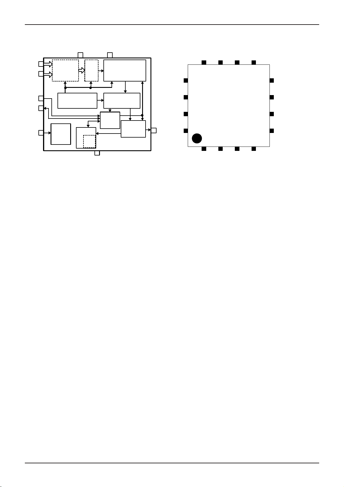
●Block Diagram, Pin configuration
AVDD DVDD
SREF
SIN[7:0]
Sensor I/F CV
translate circuit
ADC
Data corre ction and
making to format
SIN6
Technical Note
LED1
SIN2
SIN1/
LED0
LED2
SIN4
SIN5/
SIN3/
SIN7/
LED3
AVDD
DVDD
SDA
SCL
INT
SDN
SCL
SDA
SDN
Reset
generation
Conversion
sequence control
Clock
generation
CR
oscill
ation
GND
Data register
host I/F
Power
management
INT
GND
SIN0
SREF
・Sensor I/F CV translate circuit
This module selects between sensor inputs. The selection sequences between all 16 channels.
・AD Conversion
The voltage into which CV is converted is converted into a digital value. Conversion is 10 bit and full scale corresponds to AVDD.
・Conversion sequence control
Performs timing generation for the analogue circuitry and a sequencer circuit for selection of the sensor channel for conversion.
・Data correction and making to format
This module provides the digital intelligence of the sensor.
The block includes, amongst other things, scaling, adding offsets and input filtering for de-bouncing.
Registers are formatted to simplify usage by the softwareapplication.
The block implements auto-calibration to manage drift in temperature, process variation, voltage variation and aging effects.
・Data register
This stores the results for the software application. Please refer to the register map for details.
・HOST I/F
2 wire serial interface.
・Power management
The power management block provides smart power control.
When the sensors are not in use, the Controller automatically transitions into a low-power mode.
When a sensor is touched, then the device automatically wakes up and enters its normal operation.
The chip drives an INT pin for alerting the controller device in this case.
・Reset generation
The circuit is initialized by the external SDN pin.
・Clock generation
The device has an internal oscillator.
Provision is also made if the application would like to make use of an external clock input.
www.rohm.com
© 2009 ROHM Co., Ltd. All rights reserved.
3/14
2009.04 - Rev.B
BU21010MUV
Technical Note
●Pin Description
Pin
No.
Name I/O Function Note
1 SDA In/Out
2 SCL In
Communication data sending and
receiving
Communication synchronous clock
input
3 INT Out Output of interrupt
4 SDN In Shutdown input
- DVDD "Hi-Z" ⑤
- DVDD - ②
"L" : Active mode
"H" : Idle mode
"L" : Halt condition
"H" : state of operation
Supply
Reference
Reset
Level
DVDD "L" ③
DVDD - ①
5 SREF AIn Standard capacitor input - AVDD "Hi-Z" ④
6 SIN0 AIn sensor input0 - AVDD "Hi-Z" ④
7 GND Ground Analog and digital ground - - - -
8 SIN1/LED0 AIn/Out sensor input 1 / LED control output 0
sensor input , LED drive
select
AVDD "Hi-Z" ④
9 SIN2 AIn sensor input2 - AVDD "Hi-Z" ④
10 SIN3/LED1 AIn/Out sensor input 3 / LED control output 1
sensor input , LED drive
select
AVDD "Hi-Z" ④
11 SIN4 AIn sensor input4 - AVDD "Hi-Z" ④
12 SIN5/LED2 AIn/Out sensor input 5 / LED control output 2
sensor input , LED drive
select
AVDD "Hi-Z" ④
13 SIN6 AIn sensor input6 - AVDD "Hi-Z" ④
14 SIN7/LED3 AIn/Out sensor input 7 / LED control output 3
sensor input , LED drive
select
AVDD "Hi-Z" ④
15 AVDD Power Digital part Power supply - AVDD - -
I/O Pad
16 DVDD Power Analog part Power supply - DVDD - -
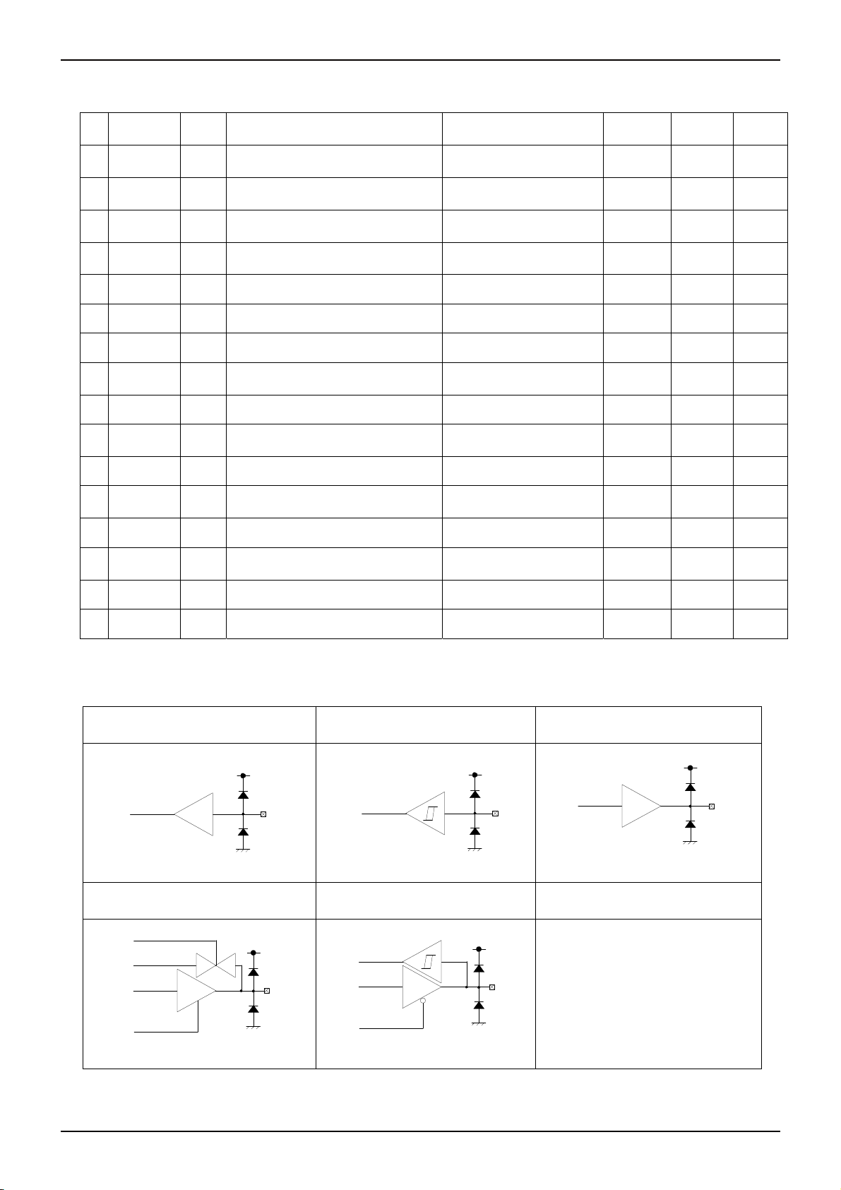
●I/O Circuit
①CMOS INPUT ②CMOS Schmitt INPUT ③CMOS OUTPUT
CIN
PAD
④CMOS 3stute OUTPUT with
ANALOG-SW
PADCIN
⑤CMOS Schmitt INOUT
I
ASW
AIN
PADI
OE
CIN
PADI
OEN
PAD
www.rohm.com
© 2009 ROHM Co., Ltd. All rights reserved.
4/14
2009.04 - Rev.B
BU21010MUV
Technical Note
●HOST I/F
・ 2 wire serial, BUS
Slave mode only
Slave Address = 5Eh
Normal (Normal mode. 100kHz Transfer rate)
Fs mode (Fast mode. 400kHz Transfer rate) also.
Not adapting sequential read / write.
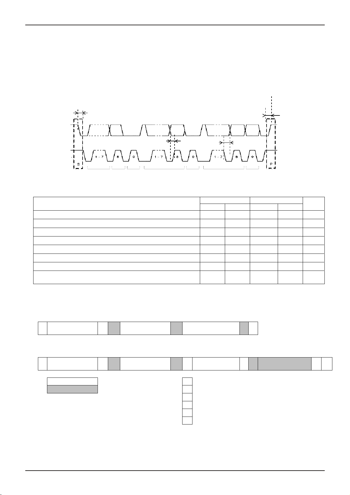
【Data format】
t
HD;STA
t
SU;STO
SDA
t
SU;DAT
t
HD;DAT
SCL
Address
Read
ACK
Data Data
ACK
ACK
Parameter
Standard mode High Speed mode
MIN MAX MIN MAX
fSCL : SCL Clock Freq 0 100 0 400 kHz
tHD;STA : START condition hold time 4.0 - 0.6 - μsec
tLOW : SCL “L” 4.7 - 1.3 - μsec
tHIGH : SCL “H” 4.0 - 0.6 - μsec
tHD;DAT : Data hold time 0.1 3.45 0.1 0.9 μsec
tSU;DAT : Data setup time 0.25 - 0.1 - μsec
tSU;STO : START condition hold time 4.0 - 0.6 - μsec
tBUF : Free time of bus between STOP condition and START
condition
4.7 - 1.3 - μsec
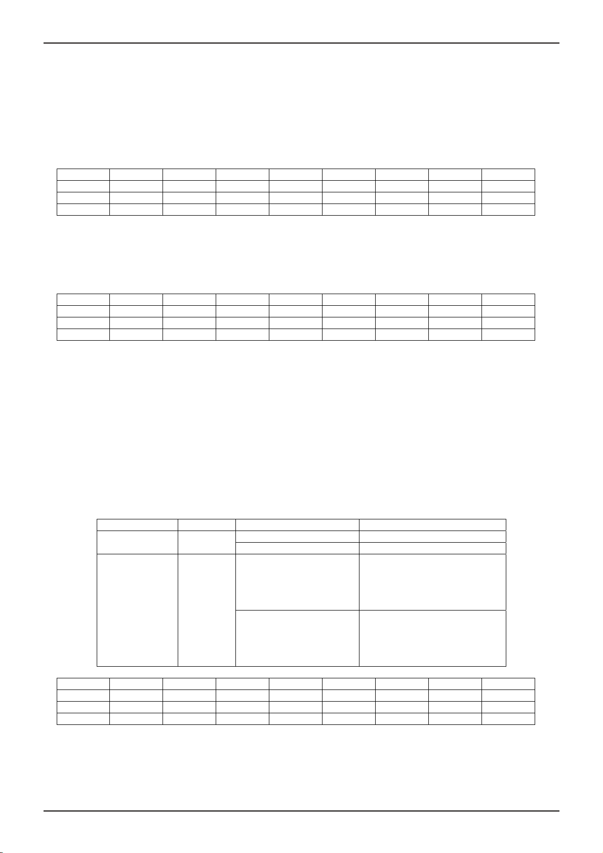
【PROTOCOL】
Unit
・Write Protocol
S SLAVE ADDRESS W
7bit = 5Eh 8bit 8bit
A
REGISTER
ADDRESS
A WRITE DATA AP
・Read Protocol
S SLAVE ADDRESS W
A
REGISTER
ADDRESS
A S SLAVE ADDRESS R A READ DATA N P
7bit = 5Eh 8bit 7bit = 5Eh 8bit
from Master to Slave S = START condition
from Slave to Master P = STOP condition
R = data direction READ (SDA HIGH)
W = data direction WRITE (SDA LOW)
A = acknowledge (SDA LOW)
N = not acknowledge (SDA HIGH)
www.rohm.com
© 2009 ROHM Co., Ltd. All rights reserved.
5/14
2009.04 - Rev.B

BU21010MUV
●Register map
Address Register name R/W Length Explanation
1*h SENS_DATA R 1byte / channel Sensor output data. One for each channel.
32h BTN R 1byte Button On/Off.
35h BTN_STATE R 1byte Button state data.
4*h OFFSET R 1byte / channel Offset correction data. One for each channel.
60h, 61h GES_VEL R 2byte Gesture duration.
62h GES_DIR R 1byte Gesture direction.
E2h GES_CLR W 1byte Gesture clear control.
E3h GES_CTL R/W 1byte Gesture control.
E4h GES_CLK R/W 1byte Gesture clock setting.
E5h GES_TIMEOUT R/W 1byte Gesture time-out data setting.
EEh CALIB W 1byte Soft calibration execution.
EFh DONE R/W 1byte Setting done command.
Technical Note
F0h SENS_CH R/W 1byte Sensor channel enables.
F2h LED_CH R/W 1byte LED channel enables.
F3h IDLE_CH R/W 1byte Idle mode release control.
F5h LED_LINK R/W 1byte LED linkage to sensor input.
F6h TIMES R/W 1byte
F7h TH_ON2 R/W 1byte
F8h TH_ON2_CH R/W 1byte Per channel selection of whether to use TH_ON or TH_ON2.
FAh CMD R/W 1byte Simultaneous press and idle mode entry.
FBh GAIN_FILTER R/W 1byte Gain setting, filter function.
FCh TH_ON R/W 1byte
FDh TH_OFF R/W 1byte
FEh DLED R/W 1byte Register to allow simple writing to LEDs.
Defines the sampling interval and number of samples
required to recognize a button press.
A second threshold value in the detection of a button going
from OFF state to ON state.
A threshold value in the detection of a button going from OFF
state to ON state.
A threshold value in the detection of a button going from ON
state to OFF state.
www.rohm.com
© 2009 ROHM Co., Ltd. All rights reserved.
6/14
2009.04 - Rev.B

BU21010MUV
【1*h : Sensor Output Data】
Name: SENS_DATA
Address: 1* h (one byte per sensor channel)
Description: The sensor output that converts to 10bit. Scaling, offsets and filtering (when enabled) are applied.
The most significant 8 bits are presented to the software with this register.
Bit7 Bit6 Bit5 Bit4 Bit3 Bit2 Bit1 Bit0
1*h SD_*[7] SD_*[6] SD_*[5] SD_*[4] SD_*[3] SD_*[2] SD_*[1] SD_*[0]
R/W R R R R R R R R
Initial val. 1 0 0 0 0 0 0 0
【32h : Button On/Off 】
Name: BTN
Address: 32h
Description: This is the state of the sensor when considered as an ON/OFF button. Here 1 : On. 0 :Off.
Bit7 Bit6 Bit5 Bit4 Bit3 Bit2 Bit1 Bit0
32h CH7 CH6 CH5 CH4 CH3 CH2 CH1 CH0
R/W R R R R R R R R
Initial val. 0 0 0 0 0 0 0 0
【35h : Button State Data】
Name: BTN_STATE
Address: 35h
Description: This provides information about the press.
CH[3:0] : Effective channel :
This indicates which button is dominant.
SIMUL : Button effective :
This indicates that the effective channel corresponds to a valid button press according to the thresholds. 1 : On. 0 : Off.
CONTINU : A push and hold is effective :
Indicates that the button was pressed and held for more than push/hold judgment time. 1 : On. 0 : Off.
Bit7 Bit6 Bit5 Bit4 Bit3 Bit2 Bit1 Bit0
35h CONTINU - - SIMUL CH[3] CH[2] CH[1] CH[0]
R/W R - - R R R R R
Initial val. 0 - - 0 0 0 0 0
【4* h : Offset Correction Data】
Name: OFFSET
Address: 4* h (one byte per sensor channel)
Description: This is the offset required to correct the sense data to half scale during the calibration procedure.
Bit7 Bit6 Bit5 Bit4 Bit3 Bit2 Bit1 Bit0
4*h OFS_*[7] OFS_*[6] OFS_*[5] OFS_*[4] OFS_*[3] OFS_*[2] OFS_*[1] OFS_*[0]
R/W R R R R R R R R
Initial val. 1 0 0 0 0 0 0 0
【60h / 61h : Gesture Duration】
Name: GES_VEL
Address: 60h, 61h
Description: Indicates the duration of the gesture in number of internal clocks.
The count is a clock set with 0xE4(GES_CLK).
It is possible to count up to 0~4095 clocks.
Gesture duration=(gesture sampling interval) * VEL [sec]
Bit7 Bit6 Bit5 Bit4 Bit3 Bit2 Bit1 Bit0
60h VEL[7] VEL[6] VEL[5] VEL[4] VEL[3] VEL[2] VEL[1] VEL[0]
61h - - - - VEL[11] VEL[10] VEL[9] VEL[8]
R/W R R R R R R R R
Initial val. 0 0 0 0 0 0 0 0
Technical Note
www.rohm.com
© 2009 ROHM Co., Ltd. All rights reserved.
7/14
2009.04 - Rev.B
BU21010MUV
【62h : Gesture Direction Judgment】
Name: GES_DIR
Address: 62h
Description: Gesture direction judgment
DIR_A : gesture direction A
0xE3(GES_CTL) reference
DIR_B : gesture direction B
0xE3(GES_CTL) reference
Bit7 Bit6 Bit5 Bit4 Bit3 Bit2 Bit1 Bit0
62h - - - - - - DIR_B DIR_A
R/W - - - - - - R R
Initial val. - - - - - - 0 0
【E2h : Gesture Clear】
Name: GES_CLR
Address: E2h
Description: This register when written to clears GES_VEL and GES_DIR.
It is cleared by one, and it returns to 0 by the automatic operation.
Bit7 Bit6 Bit5 Bit4 Bit3 Bit2 Bit1 Bit0
E2h CLR - - - - - - R/W W - - - - - - -
Initial val. 0 - - - - - - -
【E3h : Gesture Function Setting】
Name: GES_CTL
Address: E3h
Description: This register controls what key-press sequence is recognized as a gesture.
Only 4 channels may be used - SIN0, SIN2, SIN4, and SIN6.
EN : enable
These are the enable bits. One is provided for each of the 4 sense inputs used for gesture. EN[0] is for SN0, EN[1] is for
SN2, EN[2] is for SN4 and EN[3] is for SN6. 1 is to enable and 0 is for disable.
MODE : mode
0 : Requires all sensors to be present in the sequence before the gesture is recognized.(All detection mode)
1 : Allows one or more of the keys to be missed in the sequence.(Verbose mode)
The condition and the direction of detection that can be detected in each mode are as follows.
mode MODE Direction(GES_DIR) Detected
All detection 0
Verbose 1
Bit7 Bit6 Bit5 Bit4 Bit3 Bit2 Bit1 Bit0
E3h - - - MODE EN[3] EN[2] EN[1] EN[0]
R/W - - - W W W W W
Initial val. - - - 1 1 1 1 1
DIR_A 1)SIN0→SIN2→SIN4→SIN6
DIR_B 1)SIN6→SIN4→SIN2→SIN0
1)SIN0→SIN2→SIN4
2)SIN0→SIN2→ SIN6
DIR_A
DIR_B
3) SIN2→SIN4→SIN6
4)SIN0→ SIN4
5) SIN2→ SIN6
1)SIN6→SIN4→SIN2
2)SIN6→SIN4→ SIN0
3) SIN4→SIN2→SIN0
4)SIN6→ SIN2
5) SIN4→ SIN0
Technical Note
www.rohm.com
© 2009 ROHM Co., Ltd. All rights reserved.
8/14
2009.04 - Rev.B

BU21010MUV
【E4h : Gesture Clock Setting】
Name: GES_CLK
Address: E4h
Description: This register allows setting of the time base for the gesture detection.
It sets a divide ratio of the clock used.
The maximum judgment time and the sampling interval of the gesture can be set by changing this clock.
Gesture sampling interval =
1 / ( ( Internal oscillation frequency) / ( 2 * 16 * 16 ) * 1 [sec] … G_DIV = 0
1 / ( ( Internal oscillation frequency) / ( 2 * 16 * 16 ) * 2 [sec] … G_DIV = 1
1 / ( ( Internal oscillation frequency) / ( 2 * 16 * 16 ) * 4 [sec] … G_DIV = 2
1 / ( ( Internal oscillation frequency) / ( 2 * 16 * 16 ) * 8 [sec] … G_DIV = 3
Gesture maximum judgment time=(Gesture sampling interval) * TO * 16 [sec]
For example with an internal clock of 1.1MHz
G_DIV Gesture sampling interval[msec] Gesture maximum judgment time [sec]
0 0.46 1.90
1 0.93 3.81
2 1.86 7.62
3 3.72 15.2
Bit7 Bit6 Bit5 Bit4 Bit3 Bit2 Bit1 Bit0
E4h - - - - - - G_DIV[1] G_DIV[0]
R/W - - - - - - W W
Initial val. - - - - - - 1 0
【E5h : Gesture Timeout Data Setting】
Name: GES_TIMEOUT
Address: E5h
Description: The maximum judgment time of the gesture is set.
A key sequence which exceeds this time is not recognized.
Gesture Maximum Judgment Time=(Gesture sampling interval) * TO * 16 [sec]
Bit7 Bit6 Bit5 Bit4 Bit3 Bit2 Bit1 Bit0
E5h TO[7] TO[6] TO[5] TO[4] TO[3] TO[2] TO[1] TO[0]
R/W W W W W W W W W
Initial val. 1 1 1 1 1 1 1 1
【EEh : Soft Calibration】
Name: CALIB
Address: EEh
Description: This forces a chip re-calibration when a 1 is written and returns to 0 afterward automatically.
Please note that one should always re-calibrate after changing the gain adjustment value.
Bit7 Bit6 Bit5 Bit4 Bit3 Bit2 Bit1 Bit0
EEh - - - - - - - CALIB
R/W - - - - - - - W
Initial val. - - - - - - - 0
【EFh : Setting Done, Detect Start】
Name: DONE
Address: EFh
Description: This register should be written to following register updates.
Bit7 Bit6 Bit5 Bit4 Bit3 Bit2 Bit1 Bit0
EFh - - - - - - - DONE
R/W - - - - - - - W
Initial val. - - - - - - - 0
Technical Note
www.rohm.com
© 2009 ROHM Co., Ltd. All rights reserved.
9/14
2009.04 - Rev.B

BU21010MUV
Technical Note
【F0h : Sensor Channel Setting】
Name: SENS_CH
Address: F0h
Description: Individual enabling and disabling of sensor channels. 1:Effective 0:Not in use
Bit7 Bit6 Bit5 Bit4 Bit3 Bit2 Bit1 Bit0
F0h SIN7 SIN6 SIN5 SIN4 SIN3 SIN2 SIN1 SIN0
R/W W W W W W W W W
Initial val. 0 0 0 0 0 0 0 0
【F2h : LED Channel Setting】
Name: LED_CH
Address: F2h
Description: Enables and disables the channels to be used as LED outputs.
Valid for the 8 LED outputs.1:Effective 0:Not in use
Bit7 Bit6 Bit5 Bit4 Bit3 Bit2 Bit1 Bit0
F2h - - - - LED3 LED2 LED1 LED0
R/W - - - - W W W W
Initial val. - - - - 0 0 0 0
【F3h : Idle Exit Condition】
Name: IDLE_CH
Address: F3h
Description: Defines which channels cause the device to wake up – i.e. go from idle mode to normal operation on a
key press. Selection is made on a per channel basis.
1:Effective 0:Not used
Bit7 Bit6 Bit5 Bit4 Bit3 Bit2 Bit1 Bit0
F3h SIN7 SIN6 SIN5 SIN4 SIN3 SIN2 SIN1 SIN0
R/W W W W W W W W W
Initial val. 1 1 1 1 1 1 1 1
【F5h : LED to Sensor Linkage】
Name: LED_LINK
Address: F5h
Description: Allows the LED outputs to be automatically linked to the input channels without need for
any software control.
1 : It synchronizes with the button. 0 : It synchronizes with data (The register name: DLED) from host.
Bit7 Bit6 Bit5 Bit4 Bit3 Bit2 Bit1 Bit0
F5h - - - - LED3 LED2 LED1 LED0
R/W - - - - W W W W
Initial val. - - - - 1 1 1 1
【F6h : Sampling Interval and Number of Samples Used for Button Press】
Name: TIMES
Address: F6h
Description: Defines the sampling interval and number of samples required to recognise as a button press.
CONT_T[3:0] : Push and hold judgment time :
Governs how long it is before the chip decides it is push and hold. Given by the following equation:
Push-Hold Time = system clock x 2
19
x CONT_T (Example: system clock 1[MHz] time : About 520[msec]).
SAMP[3:0] : Sampling Interval :
Given by the following equation:
Sampling interval = system clock x 2
13
x SAMP (Example: system clock 1[MHz] time : About 8.2[msec]).
Bit7 Bit6 Bit5 Bit4 Bit3 Bit2 Bit1 Bit0
F6h CONT_T[3] CONT_T[2] CONT_T[1] CONT_T[0] SAMP[3] SAMP[2] SAMP[1] SAMP[0]
R/W W W W W W W W W
Initial val. 0 0 0 0 0 0 0 0
www.rohm.com
© 2009 ROHM Co., Ltd. All rights reserved.
10/14
2009.04 - Rev.B

BU21010MUV
【F7h : Button OFF→ON Threshold】
Name: TH_ON2
Address: F7h
Description: A second threshold value for determining a button off→on judgment of sensor.
The sensor output value of 8bit (register SENS_DATA) is compared with
128+ ON2 [6:0], and if it is larger, the button is determined active.
Bit7 Bit6 Bit5 Bit4 Bit3 Bit2 Bit1 Bit0
F7h - ON2[6] ON2[5] ON2[4] ON2[3] ON2[2] ON2[1] ON2[0]
R/W - W W W W W W W
Initial val. - 0 0 1 0 0 0 0
【F8h : Button OFF→ON Threshold Selection】
Name: TH_ON2_CH
Address: F8h
Description: This register is used to relate either threshold TH_ON or TH_ON2 to particular sensor channels
for button press activity determination.
1 : TH_ON2 is applied 0 :TH_ON is applied
Bit7 Bit6 Bit5 Bit4 Bit3 Bit2 Bit1 Bit0
F8h SIN7 SIN6 SIN5 SIN4 SIN3 SIN2 SIN1 SIN0
R/W W W W W W W W W
Initial val. 0 0 0 0 0 0 0 0
【FAh: Simultaneous Press and Idle Mode Entry】
Name: CMD
Address: FAh
Description:
SIMUL_SEL : Simultaneous push judgment element choice :
In the case of simultaneous key press a decision must be made to select the dominant channel. The chip allows for two
alternative methods. Either it can be based on whichever key press was first, or the priority can be based on the highest
signal level.
1 : A level of a sensor gives priority 0 : Give priority to the channel pushed earliest
INTERMIT_EN : Intermittent and the drive are enable. :
Whether intermittent is driven at the idol mode is selected.
1:Intermittent is driven. 0:Intermittent is not driven. Initial state:Intermittent is driven.
IDLE_T[3:0] : non-detect time-out setting :
This sets the time the chip takes to go from normal mode to idle mode in a period key inactivity.
Duration = system clock x 2
Bit7 Bit6 Bit5 Bit4 Bit3 Bit2 Bit1 Bit0
FAh SIMUL_SEL - - INTERMIT_EN IDLE_T[3] IDLE_T[2] IDLE_T[1] IDLE_T[0]
R/W W - - W W W W W
Initial val. 0 - - 1 0 1 1 1
【FBh : Gain Setting, Filter Function】
Name: GAIN_FILTER
Address: FBh
Description: Gain adjustment and setting of noise filter function
GAIN[2:0] : gain setting :
It uses it for the gain adjustment in eight stages. Initial adjustment value:x1
GAIN[2:0] 000 001 010 011 100 101 110 111
Adjustment value x 1 x 4.22 x 8.4 x 16.5 x 23 x 46 x 69 x 92
FILTER_EN : Filter enable :
Enables/disables setting of noise filter function
1 : enabled 0 : disabled Initial state : disabled
DELTA[3:0] : Filter follow count setting :
The follow count to which the noise filter function is effective is set.
Bit7 Bit6 Bit5 Bit4 Bit3 Bit2 Bit1 Bit0
FBh GAIN[2] GAIN [1] GAIN[0] FILTER_EN DELTA[3] DELTA[2] DELTA[1] DELTA[0]
R/W W W W W W W W W
Initial val. 0 0 0 0 0 0 1 0
19
x IDLE_T (Example of system clock 1[MHz]time : About 520[msec])
Technical Note
www.rohm.com
© 2009 ROHM Co., Ltd. All rights reserved.
11/ 14
2009.04 - Rev.B

BU21010MUV
【FCh: Switch OFF -> ON Threshold】
Name: TH_ON
Address: FCh
Description: This register provides a threshold value for determining if a sensor has transitioned from OFF to ON.
This is relative value from reference value (128d). So the absolute value of threshold is 128d + ON[6:0].
It makes a threshold value between TH_ON and TH_OFF.
TH_ON must be bigger than TH_OFF (TH_ON >= TH_OFF)
Maximum threshold is 256d and minimum value is 128d.
Bit7 Bit6 Bit5 Bit4 Bit3 Bit2 Bit1 Bit0
FCh - ON[6] ON[5] ON[4] ON[3] ON[2] ON[1] ON[0]
R/W - W W W W W W W
Initial val. - 0 0 1 0 0 0 0
【FDh: Switch ON -> OFF Threshold Value】
Name: TH_OFF
Address: FDh
Description: This register provides a threshold value for transitioning from ON to OFF.
This is relative value from reference value (128d). So absolute value of threshold is
128d + OFF[6:0]. It makes a threshold value between TH_ON and TH_OFF.
TH_OFF must be smaller than TH_ON (TH_OFF =< TH_ON)
Maximum value is 256d and minimum value is 128d.
Bit7 Bit6 Bit5 Bit4 Bit3 Bit2 Bit1 Bit0
FDh - OFF[6] OFF[5] OFF[4] OFF[3] OFF[2] OFF[1] OFF[0]
R/W - W W W W W W W
Initial val. - 0 0 0 0 0 0 1
【FEh: LED Port Data】
Name: DLED
Address: FEh
Description: When LED is not linked with the sensor, it becomes a simple digital output that controls the LED.
1 : Light. 0 : Turned off.
Bit7 Bit6 Bit5 Bit4 Bit3 Bit2 Bit1 Bit0
FEh - - - - D3 D2 D1 D0
R/W - - - - W W W W
Initial val. - - - - 0 0 0 0
Technical Note
www.rohm.com
© 2009 ROHM Co., Ltd. All rights reserved.
12/14
2009.04 - Rev.B

BU21010MUV
Technical Note
●Operation mode
This IC has a normal mode, idle mode and a shutdown mode as states of operation.
【Normal mode】
This is the normal operation of the device. Output pin INT="L".
【Idle mode】
This is the mode when the normal mode times out due to inactivity on the keys. In this mode the control interface is still
alive.
*Usually time-out is aimed at about 200msec or less.
*Transition between normal and idle modes is automatic and without software control.
【Shutdown mode】
In this mode the device is completely stopped – and reset. This is achieved by making the terminal SDN L. All analog
circuits and the logic circuits are stopped. The return from the shutdown mode returns by making the terminal SDN H.
*After shut-down all registers have their default values.
●Initialization procedure
A normal power on sequence is:
(1) Power on
(2) Setup the registers
(3) Write ‘1’ to 0xEF (done register)
<sensing operation begins after auto-calibration occurs>
●Power supply turning on procedure
You should always power on DVDD at the same time as AVDD or before AVDD.
www.rohm.com
© 2009 ROHM Co., Ltd. All rights reserved.
13/14
2009.04 - Rev.B

BU21010MUV
●Ordering part number
B U 2 1 0 1 0 M U V - E 2
Technical Note
Part No Part No Package
VQFN016V3030
<Tape and Reel information>
Quantity
Direction
of feed
0.4±0.1
1.0MAX
0.08 S
0.75
C0.2
16
13
3.0±0.1
1PIN MARK
1.4±0.1
1
12 9
3.0±0.1
S
(0.22)
+0.03
–0.02
0.5
0.02
4
5
8
1.4±0.1
+0.05
0.25
–0.04
(Unit : mm)
Packaging and forming specification
MUV : VQFN016V3030
Embossed carrier tapeTape
3000pcs
E2
The direction is the 1pin of product is at the upper left when you hold
()
reel on the left hand and you pull out the tape on the right hand
Reel
1pin
Order quantity needs to be multiple of the minimum quantity.
∗
E2:Embossed tape and reel
Direction of feed
www.rohm.com
© 2009 ROHM Co., Ltd. All rights reserved.
14/14
2009.04 - Rev.B

Notes
No copying or reproduction of this document, in part or in whole, is permitted without the
consent of ROHM Co.,Ltd.
The content specied herein is subject to change for improvement without notice.
The content specied herein is for the purpose of introducing ROHM's products (hereinafter
"Products"). If you wish to use any such Product, please be sure to refer to the specications,
which can be obtained from ROHM upon request.
Examples of application circuits, circuit constants and any other information contained herein
illustrate the standard usage and operations of the Products. The peripheral conditions must
be taken into account when designing circuits for mass production.
Great care was taken in ensuring the accuracy of the information specied in this document.
However, should you incur any damage arising from any inaccuracy or misprint of such
information, ROHM shall bear no responsibility for such damage.
The technical information specied herein is intended only to show the typical functions of and
examples of application circuits for the Products. ROHM does not grant you, explicitly or
implicitly, any license to use or exercise intellectual proper ty or other rights held by ROHM and
other par ties. ROHM shall bear no responsibility whatsoever for any dispute arising from the
use of such technical information.
Notice
The Products specied in this document are intended to be used with general-use electronic
equipment or devices (such as audio visual equipment, ofce-automation equipment, communication devices, electronic appliances and amusement devices).
The Products specied in this document are not designed to be radiation tolerant.
While ROHM always makes efforts to enhance the quality and reliability of its Products, a
Product may fail or malfunction for a variety of reasons.
Please be sure to implement in your equipment using the Products safety measures to guard
against the possibility of physical injur y, re or any other damage caused in the event of the
failure of any Product, such as derating, redundancy, re control and fail-safe designs. ROHM
shall bear no responsibility whatsoever for your use of any Product outside of the prescribed
scope or not in accordance with the instruction manual.
The Products are not designed or manufactured to be used with any equipment, device or
system which requires an extremely high level of reliability the failure or malfunction of which
may result in a direct threat to human life or create a risk of human injury (such as a medical
instrument, transpor tation equipment, aerospace machinery, nuclear-reactor controller,
fuel-controller or other safety device). ROHM shall bear no responsibility in any way for use of
any of the Products for the above special purposes. If a Product is intended to be used for any
such special purpose, please contact a ROHM sales representative before purchasing.
If you intend to export or ship overseas any Product or technology specied herein that may
be controlled under the Foreign Exchange and the Foreign Trade Law, you will be required to
obtain a license or permit under the Law.
Thank you for your accessing to ROHM product informations.
More detail product informations and catalogs are available, please contact us.
ROHM Customer Support System
www.rohm.com
© 2009 ROHM Co., Ltd. All rights reserved.
http://www.rohm.com/contact/
R0039
A
 Loading...