

Page 1
PRODUCTS
HYBRID IC
TYPE
BP3591
<Specifications (Precautions and Prohibitions)>
Precautions for Safety
●
1) The products are designed and produced for application in ordinary electronic equipment (AV equipment,
OA equipment, telecommunication equipment, home appliances, amusement equipment, etc.).
If the products are to be used in devices requiring extremely high reliability (medical equipment,
transport equipment, aircraft/spacecraft, nuclear power controllers, fuel controllers, car equipment
including car accessories, safety devices, etc.) and whose malfunction or operational error may endanger
human life and sufficient fail-safe measures, please consult with the ROHM sales staff in advance. If
product malfunctions may result in serious damage, including that to human life, sufficient fail-safe
measures must be taken, including the following:
[a] Installation of protection circuits or other protective devices to improve system safety
[b] Installation of redundant circuits in the case of single-circuit failure
2) The products are designed for use in a standard environment and not in any special environments.
Application of the products in a special environment can deteriorate product performance. Accordingly,
verification and confirmation of product performance, prior to use, is recommended if used under the
following conditions:
[a] Use in various types of liquid, including water, oils, chemicals, and organic solvents
[b] Use outdoors where the products are exposed to direct sunlight, or in dusty places
[c] Use in places where the products are exposed to sea winds or corrosive gases, including
, H2S, NH3, SO2, and NO2
Cl
2
[d] Use in places where the products are exposed to static electricity or electromagnetic waves
[e] Use in environment subject to strong vibration and impact.
[f] Use in proximity to heat-producing components, plastic cords, or other flammable items
[g] Use involving sealing or coating the products with resin or other coating materials
[h] Use of the products in places subject to dew condensation
3) The products might receive the radio wave interference from electronic devices such as Wireless LAN
devices, Bluetooth devices, digital cordless telephone, microwave oven and so on that radiate
electromagnetic wave.
4) The products are not radiation resistant.
5) Verification and confirmation of performance characteristics of products, after on-board mounting, is
advised.
6) Confirm that operation temperature is within the specified range described in product specification.
7) Failure induced under deviant condition from what defined in the product specification can not be
guaranteed.
8) This product is a specification to radiate the radio wave. It is necessary to acquire the attestation of
decided Radio Law of each region used to use the equipment that radiates the radio wave.
Please inquire about the attestation of Radio Law that this product acquires.
9) When product safety related problems arises, please immediately inform to ROHM, and consider
technical counter measure.
PAGE
1/19
DESIGN CHECK APPROVAL
TSZ22111・04・002
DATE: 21/FEB./2012
REV.B
SPECIFICATION No.:BP3591-B-001-E(Lead Free)
Page 2
PRODUCTS
HYBRID IC
<Specifications (Precautions and Prohibitions)>
●Precautions for Reference Circuits
1) If change is made to the constant of an external circuit, allow a sufficient margin due to variations of the
characteristics of the products and external components, including transient characteristics, as well as
static characteristics.
2) The reference circuit examples, their constants, and other types of information contained herein are
applicable only when the products are used in accordance with standard methods. Therefore, if mass
production is intended, sufficient consideration to external conditions must be made.
Precaution for Electrostatic
●
This product is Electrostatic sensitive product, which may be damaged due to Electrostatic discharge.
Please take proper caution during manufacturing and storing so that voltage exceeding Product maximum
rating won't be applied to products. Please take special care under dry condition (Grounding of human
body / equipment / solder iron, isolation from charged objects, setting of Ionizer, friction prevention and
temperature / humidity control etc.)
● Precaution for Storage / Transportation
1) Product performance and connector mating may deteriorate if the products are stored in the following
places:
[a] Where the products are exposed to sea winds or corrosive gases, including Cl
and NO
2
[b] Where the temperature or humidity exceeds those recommended by the Company
Temperature: 5℃~40℃, Humidity 40%~60%
[c] Storage in direct sunshine or condensation.
[d] Storage in high Electrostatic.
2) Even under ROHM recommended storage condition, connector mating of products over 1 year old
may be degraded.
3) Store / transport cartons in the correct direction, which is indicated on a carton as a symbol, otherwise
bent leads may occur due to excessive stress applied when dropping of a carton..
Precaution for Product Label
●
QR code printed on ROHM product label is only for internal use, and please do not use at customer site.
It might contain a internal part number that is inconsistent with an product part number.
Precaution for Disposition
●
When disposing products please dispose them properly with a industry waste company.
Precaution for Foreign Exchange and Foreign Trade Act
●
Note: Since concerned goods are fallen under controlled goods prescribed by Foreign exchange and Foreign
trade act, the permission based on the act is necessary in case of export. Please follow the necessary
procedures based on relevant laws and regulations when end goods, which were manufactured by your
company with the concerned goods, are brought to foreign countries or nonresident.
TYPE
BP3591
PAGE
2/19
, H2S, NH3, SO2,
2
TSZ22111・05・002
REV.B
SPECIFICATION No.:BP3591-B-001-E(Lead Free)
Page 3
PRODUCTS
!
● Prohibitions Regarding Industrial Property
1) These Specifications contain information related to the ROHM industrial property. Any use of them
other than pertaining to the usage of appropriate products is not permitted. Duplication of these
Specifications and its disclosure to a third party without the Company’s permission is prohibited.
2) Information and data on products, including application examples, contained in these specifications are
simply for reference; the Company does not guarantee any industrial property rights, intellectual
property rights, or any other rights of a third party regarding this information or data. Accordingly, the
Company does not bear any responsibility for:
[a] infringement of the intellectual property rights of a third party
[b] any problems incurred by the use of the products listed herein.
3) The Company prohibits the purchaser of its products to exercise or use the intellectual property rights,
industrial property rights, or any other rights that either belong to or are controlled by the Company, other
than the right to use, sell, or dispose of the products.
● Other Matters
1) Please sign these Specifications and return one copy to the Company.
If a copy is not returned within three months after the issued date specified on the front page of these
Specifications, the Company will consider the Specifications accepted.
2) If any matter related to these Specifications needs to be clarified, discussions shall be held promptly
between the two parties concerned to determine the issue.
HYBRID IC
<Specifications (Precautions and Prohibitions)>
TYPE
BP3591
PAGE
3/19
TSZ22111・05・002
REV.B
SPECIFICATION No.:BP3591-B-001-E(Lead Free)
Page 4
PRODUCTS
HYBRID IC
TYPE
BP3591
PAGE
4/19
1. STRUCTURE
P.C.BOARD ASSEMBLY
2. PRODUCTS
HYBRID INTEGRATED CIRCUIT
3. TYPE
BP3591
4. APPLICATION
COMMUNICATION APPLIANCE
5. FUNCTION
WIRELESS LAN COMMUNICATION
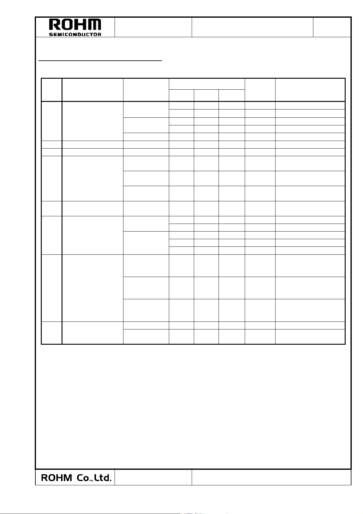
6. ABSOLUTE MAXIMUM RATINGS
No. PARAMETER SYMBOL LIMITS UNIT REMARKS
1
Power supply voltage
2 Operating temperature range Topr
3 Storage temperature range Tstg
VCC
-0.3 ~ +3.6
V DC
-40 ~ 85 ℃ -
-40 ~ 85 ℃ -
Note) These are the values that must not be exceeded at any time under any application or any test conditions.
Please make design keeping enough margins accordingly.
7. RECOMMENDED OPERATING CONDITIONS
No. PARAMETER SYMBOL
MIN. TYP. MAX.
SPEC
UNIT REMARKS
1 Power supply voltage VCC 3.1 3.3 3.5 V 2 Operating temperature range Ta -40 25 85
℃
-
TSZ22111・05・002
REV.B
SPECIFICATION No.:BP3591-B-001-E(Lead Free)
Page 5
Y
PRODUCTS
HYBRID IC
TYPE
PAGE
BP3591
8. MAIN CHARACTERISTICS
No. PARAMETER CHARACTERISTICS
5/19
1 Frequency width
2,400MHz ~ 2,483.5 MHz(ch1~ch13)
2 Frequency tolerance WITHIN ±25ppm
IEEE802.11b: 15dBm±2dB
3 RF output power (*1)
IEEE802.11g: 13dBm±2dB
IEEE802.11n: 12dBm±2dB
IEEE802.11b: 1 ~ 11Mbps
4 Supported data rates
IEEE802.11g: 6 ~ 54Mbps
IEEE802.11n: 6.5 ~ 72.2Mbps
IEEE802.11b: -94dBm @1Mbps, -89dBm @11Mbps
5 Receiving sensitivity (*1)
IEEE802.11g: -92dBm @6Mbps, -73dBm @54Mbps
IEEE802.11n: -90dBm @6.5Mbps, -68dBm @72.2Mbps
6 Security function 64bit/128bit WEP, TKIP, AES (*2)
USB2.0 (High-Speed mode)
7 Host Interface
SDIO Ver.2.00 (High-Speed mode)
UART (~921600bps)
8 Power supply voltage SINGLE 3.3V
(*1) RF output power and receiving sensitivity are performance value that is at the electricity supplying point for
antenna (antenna terminal of BP3580) in the below figure.
(*2) 64bit/128bit WEP, TKIP, and AES are everything processed with hardware.
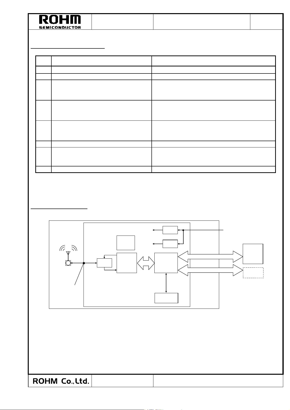
9. BLOCK DIAGRAM
BP3591
Chip Antenna
Connector
Ele ctricit y
supplying point
for antenna
BP3580
RF-SW
40MHz
OSC
RF IC
2.8V
1.2V
RF I/ F
LDO
LDO
BaseBand
&
MAC
EEPROM
HOST I/ F
FLASH I/F
3.3V
HOST
CPU
FLASH
MEMOR
Fig 1. Block diagram
・ A Flash memory (option) is necessary for use the flash boot function.
・ There is a switch type coaxial connector (MS-156C made by Hirose electric Co., Ltd.) between BP3580 and
chip antenna. Please connect an external antenna to this connector if it is necessary.
(The chip antenna cannot use when an external antenna is used.)
REV.B
SPECIFICATION No.:BP3591-B-001-E(Lead Free)
TSZ22111・05・002
Page 6
PRODUCTS
HYBRID IC
TYPE
BP3591
10. ELECTRICAL CHARACTERISTICS
CONDITIONS:Ta=25℃, VCC=3.3V, GND=0.0V
SPEC
No. PARAMETER CONDITION
UNIT REMARKS
MIN. TYP. MAX.
240 300 360 mA Continuous
280 340 400 mA Continuous (With USB)
160 200 240 mA 200 240 280 mA With USB
1 Consumption current
Sending
Receiving
Sleep mode - 500 - uA -
2 Center frequency - 2412 - 2472 MHz 3 Frequency deviation - -25 - 25 ppm -
At electricity supplying
point for antenna
At electricity supplying
point for antenna
At electricity supplying
point for antenna
nd
Side-lobe
4 RF output power
5
6
Unnecessary
out-of-band radiation
Transmit spectrum
mask
11b:11Mbps
11g:54Mbps
11n:MCS7
13 15 17 dBm
11 13 15 dBm
10 12 14 dBm
- - - 2.5 uW/MHz -
DSSS 11Mbps
OFDM
54Mbps
- - -30 dBr 1st Side-lobe
- - -50 dBr 2
- - -20 dBr ±11MHz
- - -28 dBr ±20MHz
- - -40 dBr ±30MHz
PER<8%
11b:11Mbps
- -89 -76 dBm
At electricity supplying
point for antenna
PER<10%
7 Receiving sensitivity
11g:54Mbps
-73 -65 dBm
At electricity supplying
point for antenna
PER<10%
11n:MCS7
- -68 -64 dBm
At electricity supplying
point for antenna
Unnecessary
8
radiation
for receiving
Fr<1GHz - - 4 nW -
Fr≧1GHz
- - 20 nW -
PAGE
6/19
TSZ22111・05・002
REV.B
SPECIFICATION No.:BP3591-B-001-E(Lead Free)
Page 7

PRODUCTS
11. TERMINAL FUNCTIONS
Back side
TYPE
HYBRID IC
BP3591 Connector (Socket) Type
:AXK5F34347YG (Panasonic Electric Works Co., Ltd.)
BP3591
PAGE
7/19
34 18
1 17
No.
TERMINAL
NAME
1 SDDATA1 I/O SDIO data 1 or UART_RTS
2 SDDATA0 I/O SDIO data 0 or UART_CTS
3 GND - Ground 4 GND - Ground 5 USB_DM AI/O USB data minus 6 USB_DP AI/O USB data plus 7 SDCLK I SDIO clock 8 VCC I Power supply 3.3V Module power supply input
9 NC - None connection OPEN
10 SDCMD I/O SDIO command 11 SDDATA3 I/O SDIO data 3 12 SDDATA2 I/O SDIO data 2 13 UART_RXD I UART receiving data 14 UART_TXD O UART sending data 15 BOOT_SEL1 I(*) BOOT_SEL [1:0]
16 BOOT_SEL0 I(*)
17 HOST_SEL I(*) Host I/F select 0:USB, 1:SDIO
18 FLASH_RXD I Flash memory receiving data Terminal for flash boot
19 FLASH_CSB O Flash memory selection Terminal for flash boot
20 FLASH_CLK O Flash memory clock Terminal for flash boot
21 FLASH_TXD I/O Flash memory sending data Terminal for flash boot
22 FLASH_SEL I(*) Flash memory area select 0:Area0, 1:Area1
23 GPIO0 I/O General purpose Input/Output 0 24 GPIO1 I/O General purpose Input/Output 1 25 M_ANA AI/O Analog monitor terminal Terminal for debug
26 GPIO2 I/O General purpose Input/Output 2 27 GPIO6 I/O General purpose Input/Output 6 28 HRST I Host reset 0:Reset, 1:Normal
29 PRST I Power on reset 0:Reset, 1:Normal
30 TMS I ARM JTAG TMS For debug
31 TCK I ARM JTAG TCK For debug
32 TDI I ARM JTAG TDI For debug
33 TDO O ARM JTAG TDO For debug
34 TRSTB I ARM JTAG TRSTB For debug
I/O FUNCTIONS REMARKS
User-side Connector (header) Type
:AXK6F34347YG(Panasonic Electric Works Co., Ltd.)
Table 1. Module Terminal Functions
Boot mode select
00:USB, 01:SDIO,10:FLASH,11:UART
TSZ22111・05・002
REV.B
SPECIFICATION No.:BP3591-B-001-E(Lead Free)
Page 8

PRODUCTS
(*) FLASH_SEL/HOST_SEL/BOOT_SEL0/BOOT_SEL1 terminal hold the value after reset (Power On
Reset). After reset, these terminals are used for another purpose in the module.
They have pull down resistance inside. Therefore, please set these terminals OPEN in case of setting for “0”
and Pull up 3.3V (power supply voltage) with 3kΩ~5kΩ(recommendation is 4.7 kΩ) in case of setting for “1”.
When the host MCU controls these terminal, please do not connect directly with output pin of host MCU and
insert 3kΩ~5kΩ resistor (recommendation is 4.7kΩ) between them.
PRST is POWER ON RESET terminal. It is connected 4.7kΩ+2.2uF at 3.3V inside the module.
In case that need to watch the power supply voltage, please connect such as OPEN DRAIN RESET IC for this
terminal.
Please open the other unused terminal.
HYBRID IC
TYPE
BP3591
PAGE
8/19
TSZ22111・05・002
REV.B
SPECIFICATION No.:BP3591-B-001-E(Lead Free)
Page 9

12. DIMENSIONS
PRODUCTS
HYBRID IC
TYPE
BP3591
PAGE
9/19
123*
13. MARKING PCB SPEC
Marking
Fig.3 Marking PCB SPEC(Unit: mm)
Fig.2 Dimensions(Unit: mm)
123*
: ROHM Trade Mark
BP3591 : Type Name
123* : Production lot number (3 digits)
(Example)123*→Year 2011 Week 23 *Location
(internal serial number)
REV.B
SPECIFICATION No.:BP3591-B-001-E(Lead Free)
TSZ22111・05・002
Page 10

PRODUCTS
14. PRECAUTIONS FOR MOUNTING
(1) Please don’t patterning the area under pattern prohibition area so that there is an adverse effect in a wireless
(2) Please do not set your substrates around the chip antenna within 1cm.
(3) Please do not use metals for a chassis setting this module.
(4) Please do not mount parts under this module except a specified connector.
ABOUT THE FIXATION OF THE MODULE
5.7
5.7
3.2
3.2
characteristic.
Please use the M2 screw (made of metal) for fixing BP3591.
Please use a spacer (made of metal) which height is 1.5mm, between your substrate and this module.
M2 screw hole is GND of BP3591. Please use a metal spacer for ground connection between BP3591 GND
and your substrate GND. ( Refer to the figure below)
A torque to tighten M2 screw should be more than 1kgf・cm, and do not tighten the screw too much.
Chip Antenna
Spacer
Chip Antenna
チップアンテナ 配線禁止領域 M2ネジ穴
チップアンテナ 配線禁止領域 M2ネジ穴
24.0±0.5
24.0±0.5
HYBRID IC
Pattern Prohibition Area
6.6
6.6
33.1±0.5
33.1±0.5
Shield Case
シールドケース
シールドケース
Fig.4 Precautions for Mounting (Unit:mm)
M2 screw
Fig.5 Fixed Module Figure (Side view)
Nut
TYPE
BP3591
Screw Hole (M2)
2.5
2.5
Connector
コネクタ
コネクタ
BP3591
User side PCB
2.5
2.5
24.0
24.0
PAGE
10/19
TSZ22111・05・002
REV.B
SPECIFICATION No.:BP3591-B-001-E(Lead Free)
Page 11

PRODUCTS
15. PRODUCT LABEL SPEC
HYBRID IC
TYPE
The label shown in the following figure is put on the shield case.
Technical agreement mark
for Japanese Radio Low
*Micro QR code has the MAC address information.
(Note)The design of product label might change without previous notice.
Type name
BP3591
003WWA100913
FCC ID:ANSBP3591
Fig.6 Product Label Spec
BP3591
PAGE
11/19
Micro QR code
Certification number
for Japanese Radio Low
FCC ID for USA Radio Low
MAC address
TSZ22111・05・002
REV.B
SPECIFICATION No.:BP3591-B-001-E(Lead Free)
Page 12

PRODUCTS
HYBRID IC
TYPE
BP3591
16. REFERENCE CIRCUIT
16.1 USB
*About USB_DP and USB_DM Lines
・ Please shorten the wiring length as much as possible.
・ Please take the differential impedance matching to 90Ω±10%.
・ Please set up to 45Ω±10% for impedance matching of single end.
・ Please wire USB_DP and USB_DM lines same lengths as possible.
・ Please do not bend USB lines many times and make the bend angle small.
・ Please do not make threw hole in wiring if possible.
・ Please do not cross the USB lines and another signal lines.
・ Please do not cross the USB lines and a power supply line.
*Please reduce the ripple of power supply (VCC=3.3V) as much as possible. (less than 10mVpp)
HOST INTERFACE
USB Host Interface Reference Circuit
BP35
(Difference of the length is less than 0.5mm.)
Fig.6
Fig.7
USB Interface Reference Circuit
PAGE
12/19
TSZ22111・05・002
REV.B
SPECIFICATION No.:BP3591-B-001-E(Lead Free)
Page 13

16.2 SDIO HOST INTERFACE
PRODUCTS
HYBRID IC
TYPE
BP3591
PAGE
13/19
BP3591
Fig.8 SDIO Interface Reference Circuit
*Please reduce the ripple of power supply (VCC=3.3V) as much as possible. (less than 10mVpp)
*About the line of SDCLK/SDDATA/SDCMD
・Over shoot and under shoot of signal lines cause a lot of damage to wireless performance.
Please design so that its noise level becomes lower as possible within the SDIO standard timing.
For example it can be insert dumping resistor near the host signal source.
TSZ22111・05・002
REV.B
SPECIFICATION No.:BP3591-B-001-E(Lead Free)
Page 14

16.3 UART INTERFACE
PRODUCTS
HYBRID IC
TYPE
BP3591
PAGE
14/19
BP3591
MAX3232EUE+
MAX3232EUE+
TSZ22111・05・002
REV.B
(MAXIM)
Fig.9 UART Interface Reference Circuit
SPECIFICATION No.:BP3591-B-001-E(Lead Free)
Page 15

PRODUCTS
HYBRID IC
16.4
FLASH BOOT (UART INTERFACE MODE)
TYPE
BP3591
PAGE
15/19
S25FL032P (SPANSION)
or
M25PE40 (MICRON) (*)
16.5 Reset IC
BP3591
(*) Flash memory of above figure is S25FL032P.
Fig.10 Flash Boot (UART INTERFACE )Reference Circuit
(ROHM)
BP3591
Fig.11 Reset IC Connection Reference Circuit
TSZ22111・05・002
REV.B
SPECIFICATION No.:BP3591-B-001-E(Lead Free)
Page 16

② ③
⑦
④
PRODUCTS
HYBRID IC
TYPE
BP3591
17. PACKING SPEC
17.1 Packing Method
In principle, 20 pieces of modules should be packaged in the packaging tray, and it should be piled up 5 steps
to make 100 pieces, and with an empty pack on the top.
The number of piling might change according to the quantity of delivery without previous notice.
Tray
Fixed by adhesive cellophane tape.
(4 places)
Packing case
Fixed by adhesive cellophane tape.
PAGE
16/19
Fig.12 Packing Method
17.2 Label indication
The label with following things is stuck at the packing case.
① Type name(BP3591)
② Quantity
③ Lot No.
④ Shipment inspection stamp
⑤ Country of origin
⑥ Manufacturing company name(Trade mark)
⑦ Logotype of lead free
Please refer to the following example of the label indication.
①
F
⑤
CHINA
⑥
④
Fig.13 Label Indication
(2 places)
S.MIZUHARA
TSZ22111・05・002
REV.B
SPECIFICATION No.:BP3591-B-001-E(Lead Free)
Page 17

PRODUCTS
18. MANUFACTURING FACTORY
HYBRID IC
TYPE
BP3591
PAGE
17/19
ROHM APORO CO., LTD. (FUKUOKA, JAPAN)
ROHM ELECTRICS DALIAN CO., LTD. (DALIAN, CHINA)
19. OPERATING PRECAUTIONS
1)There is some case that the MAC address does not become sequential number in a same package.
2)About soldering of mounting parts on this product, presence of soldering fillet does not be asked.
3)About the products label, defections does not be asked except coming off, lapping, or not to recognize the
characters extremely.
4)A connector is possible to break by excessive swing or shock because of the structure of the product.
Efficient evaluation is necessary to use the module when there is a fear of swinging or shocking.
5)The connector of BP3591 does not have a specification assumed to do many times of extraction and insertion.
Please be sure that the number of extraction and insertion is within 10 times.
6)There are some cases that the spring elasticity of inside the connector is lost and built-in antenna cannot be
used, if it connects an external antenna with the coaxial connector of BP3591 (external antenna connector)
for a long time.
Please do not use external antenna together with built-in antenna.
20. PRECAUTIONS AS RESRT OPERATION
・Please do not reset (PRST, HRST, COMMAND RESET) when BP3591 is accessing to its internal EEPROM.
・BP3591 under writing to the EEPROM is reset (*), which may cause unexpected failure such as incorrect
checksum.
・BP3591 under reading from the EEPROM is reset (**), which may cause unstable condition, and you should
supply VCC power again.
(*) About write operations of the EEPROM
BP3591 writes to the EEPROM in the following cases.
①Recording the MAC address
②Recording various settings used in TCP/IP firmware
③Recording credential data which is obtained when BP3591 with stand-alone mode acts WPS
(**) About read operations of the EEPPROM
BP3591 reads from the EEPROM in the following cases.
①After reset (≦100ms)
②After firmware starting (≦100ms)
③When WID_SERIAL_NUMBER command is issued.
TSZ22111・05・002
REV.B
SPECIFICATION No.:BP3591-B-001-E(Lead Free)
Page 18

PRODUCTS
HYBRID IC
TYPE
PAGE
BP3591
21. PRECAUTIONS AS A WIRELESS EQUIPMENT
BP3591 acquired “Construction design attestation” (Article 38-24, Clause1 of Radio Law in Japan) of
“Particular wireless equipment: Low power data communications system in the 2.4GHz band, which is a
Wireless equipment in Article 2-1(19)”
Therefore, only in Japan, it is possible to use as wireless equipment without applying for wireless office.
・Construction design attestation No.:003WWA100913
Be sure to keep following notes to use the module safely as wireless equipment.
1)The label on the module is a certification which shows it has “Certification of technical standard conformity.”
Please do not remove the label or do not put another label on the label.
2)Please do not resolve or remodel strictly because there are some cases of receiving penalty based on Radio Law.
3)Please use the antenna of the certification settlement※ when you use an external antenna.
※ About a certification settlement antenna
BP3591 has following certification of external antenna.
・ AA2402A-MS156CLP (Made by Antenna Technology Inc.)
・ AA2402AU-MS156CLP(Made by Antenna Technology Inc.)
Please ask separately about attested external antennas other than the above.
22. PRECAUTIONS AS A WIRELESS EQUIPMENT2.
BP3591 acquired Federal Communications Commission (FCC Part15 Subpart C).
As long as using chip antenna, your set include BP3591 is able to use in U.S. without application of FCC.
・ FCC ID: ANSBP3591
Please following the below precautions for using BP3591 as wireless equipment in U.S.
1) The label put on the product is a certification label shown to be acquiring "FCC certification".
Please do not remove the label or do not put another label on the label.
2) If FCC ID displayed on BP3591 cannot be seen from the outside, the following displays (*) are
needed for your product containing BP3591.
“Contains Transmitter Module FCC ID: ANSBP3591”
or
“Contains FCC ID: ANSBP3591”
(*) The character size can be read easily is required. However it is not required more than 8 points.
And also line break is not permit.
18/19
TSZ22111・05・002
REV.B
SPECIFICATION No.:BP3591-B-001-E(Lead Free)
Page 19

PRODUCTS
HYBRID IC
TYPE
PAGE
BP3591
3) It is necessary to display the following texts on your product. (*)
This device complies with part 15 of the FCC Rules. Operation is subject to the following two conditions:
(1) This device may not cause harmful interference, and (2) this device must accept any interference
received, including interference that may cause undesired operation.
(*) If the text cannot be displayed on your product, you should describe in a manual or a package. It is
foundations that the text is indicated on a product.
4) It is necessary to indicate all the texts applicable to the manual of your product.
① It is necessary text for all products.
FCC CAUTION
Change or modifications not expressly approved by the party responsible for compliance could void the
user’s authority to operate the equipment.
② It is necessary text for all products. 2
This transmitter must not be co-located or operated in conjunction with any other antenna or transmitter.
③ A product needs a SAR examination is necessary to indicate the following texts in a manual.
A SAR examination is not required at mobile products (*) but is required at portable products.
(*) Mobile product ・・・ The product is used separating from a human body over 20 cm.
(**) Portable product ・・・ The product is used by human body within 20cm.
③-1 It is necessary texts for a mobile product.
This equipment complies with FCC radiation exposure limits set forth for an uncontrolled environment and
meets the FCC radio frequency (RF) Exposure Guidelines in Supplement C to OET65. This equipment
should be installed and operated keeping the radiator at least 20cm or more away from person’s body
(excluding extremities: hands, wrists, feet and ankles).
③-2 It is necessary text for a portable product.
The available scientific evidence does not show that any health problems are associated with using low
power wireless devices. There is no proof, however, that these low power wireless devices are absolutely
safe. Low Power Wireless devices emit low levels of radio frequency energy (RF) in the microwave range
while being used. Whereas high levels of RF can produce health effects (by heating tissue), exposure of
low-level RF that does not produce heating effects causes no known adverse health effects. Many studies
of low-level RF exposures have not found any biological effects. Some studies have suggested that some
biological effects might occur, but such findings have not been confirmed by additional research.
[Product name(model name)] has been tested and found to comply with FCC radiation exposure limits
set forth for an uncontrolled environment and meets the FCC radio frequency (RF) Exposure Guidelines
in Supplement C to OET65. The maximum SAR levels tested for [Product name(model name)] has been
shown to be [SAR measurement value] W/kg at Body.
FCC does not request to mention of a SAR measurement value.
If you use it in an occupational environment, please change the sentence "Uncontrolled" into "Controlled".
19/19
TSZ22111・05・002
REV.B
SPECIFICATION No.:BP3591-B-001-E(Lead Free)
 Loading...