

!
!
Compact Video Driver Series for DSCs and Portable Devices
!
ESD
TECHNICAL NOTE
Ultra-compact Waferlevel
Resistance
Chip Size Packeage
Now available
Single Output Video Drivers
BH76906GU, BH76909GU, BH76912GU, BH76916GU, BH76706GU
ͶDescription
Due to a built-in charge pump circuit, this video driver does not require the large capacity tantalum capacitor at the video
output pin that is essential in conventional video drivers. Features such as a built-in LPF that has bands suited to mobile
equipment, current consumption of 0 μA at standby, and low voltage operation from as low as 2.5 V make it optimal for digital
still cameras, mobile phones, and other equipment in which high density mounting is demanded.
ͶFeatures
1) ! WLCSP ultra-compact package (1.6 mm x 1.6 mm x 0.75 mm)
2) ! Improved noise characteristics over BH768xxFVM series
3) ! Four video driver amplifier gains in lineup: 6 dB, 9 dB, 12 dB, 16.5 dB
4) Large output video driver of maximum output voltage 5.2 Vpp. Ample operation margin for supporting even low
voltage operation
5) Output coupling capacitor not needed, contributing to compact design
6) Built-in standby function and circuit current of 0 μA (typ) at standby
7) Clear image playback made possible by built-in 8
8) Due to use of bias input format, supports not only video signals but also chroma signals and RGB signals
9) Due to built-in output pin shunt switch, video output pin can be used as video input pin (BH76706GU)
ͶApplication
Mobile phone, digital still camera, digital video camera, hand-held game, portable media player
ͶLineup
Product Name Video Driver Amplifier Gain
BH76906GU 6dB 1Vpp
BH76909GU 9dB 0.7Vpp
BH76912GU 12dB 0.5Vpp
BH76916GU 16.5dB 0.3Vpp
BH76706GU 6dB 1Vpp ͵
th
-order 4.5 MHz LPF
Recommended
Input Level
Video Output Pin Shunt Function
ͶAbsolute Maximum Ratings (Ta = 25 °C)
Parameter Symbol Rating Unit
Supply voltage Vcc 3.55 V
Power dissipation Pd 580 mW
Operating temperature range Topr
Storage temperature range Tstg
ͰWhen mounted on a 50 mm58 mm1.6 mm glass epoxy board, reduce by 5.8mW/°C above Ta=+25°C.
-40+85
-55+125
Nov.2006

ͶOperating Range
Parameter Symbol Min. Typ. Max. Unit
Supply voltage Vcc 2.5 3.0 3.45 V
ͶElectrical Characteristics
[Unless otherwise specified, Ta = 25 °C, VCC = 3V]
Parameter Symbol
Circuit current 1-1 I
76906 76909 76912 76916 76706
15.0 mA In active mode (No signal)
CC1-1
Typical Values
Unit Measurement Conditions
In active mode
Circuit current 1-2 I
17.0 mA
CC1-2
(Outputting NTSC color bar
signal)
0
8
23
ԜA
In standby mode
In input mode (Applying B3 = 1.5
ԜA
V)
ԜA
Applying B3 = 3.0 V
V Standby mode
ԜA
Applying B3 = 3.0 V
ԜA
Applying B3 = 1.5 V
ԜA
Applying B3 = 0 V
V Standby mode
V Input mode
V Active mode
Circuit current 2 I
Circuit current 3 I
Standby switch input current
High Level
Standby switch switching voltage
High Level
Standby switch switching voltage
Low Level
Standby switch outflow current
High Level
Standby switch outflow current
Middle Level
Standby switch outflow current
Low Level
Mode switching voltage
High Level
Mode switching voltage
Middle Level
Mode switching voltage
low Level
0.0
CC2
CC3
I
45
thH1
1.2V min V Active mode
V
thH1
V
0.45Vmax
thL1
I
thH2
I
thM2
I
thL2
V
thH2
V
thM2
V
thL2
100
VCC
-0.2
(MIN.)
VCC/2
(TYP.)
0.2
(MAX.)
Voltage gain GV 6.0 9.0 12.0 16.5 6.0 dB Vo=100kHz, 1.0Vpp
Maximum output level Vomv 5.2 Vpp f=10kHz,THD=1%
Frequency characteristic 1 Gf1 -0.2 -0.2 dB f=4.5MHz/100KHz
Frequency characteristic 2 Gf2 -1.5 -1.4 dB f=8.0MHz/100KHz
Frequency characteristic 3 Gf3 -26 -28 dB f=18MHz/100KHz
Frequency characteristic 4 Gf4 -44 -48 dB f=23.5MHz/100KHz
o=1.0Vp-p
V
Differential gain DG 0.5 %
Inputting standard staircase
Signal
o=1.0Vp-p
V
Differential phase DP 1.0 deg
Inputting standard staircase
signal
z6MHz band
Y signal to noise ratio SNY +74 +73 +70 +70 +74 dB
C AM signal to noise ratio SNCA +77 +76 +75 +75 +77 dB
C PM signal to noise ratio SNCP +65 dB
Current able to flow into output pin lextin 30㩷 mA
50
Output DC offset Voff
max
Input impedance Rin 150
Output pin shunt switch
on resistance
Ron
3
100 kH
Inputting 100 white video signal
100500 kH
Inputting 100 chroma video signal
100500 kH
Inputting 100 chroma video signal
z band
z band
Applying 4.5 V to output pin
through 150 Ԉ
With no signal
mV
Voff = (Vout pin voltage) 2
Measure inflowing current when
kԈ
applying A3 = 1 V
Ԉ
2/16
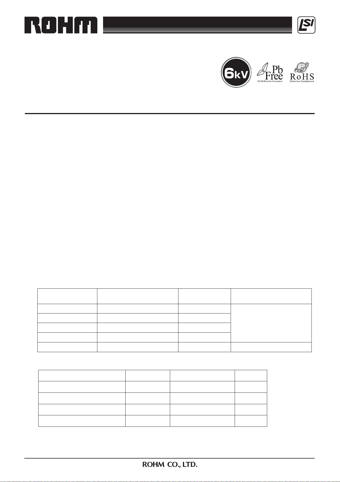
ͶTest Circuit Diagram
㪘㪊㩷
㪙㪊㩷
㪚㪊
㪘㪈㩷
㪙㪈㩷
㪚㪈㩷
㪘㪉㩷
㪚㪉㩷
㪘㪊㩷
㪙㪊㩷
㪚㪊㩷
㪘㪈㩷
㪙㪈㩷
㪚㪈㩷
㪘㪉㩷
㪘㪊㩷
㪙㪊㩷
㪚㪊
㪘㪈㩷
㪙㪈㩷
㪚㪈㩷
㪘㪉㩷
㪚㪉㩷
㪘㪊㩷
㪙㪊㩷
㪚㪊㩷
㪘㪈㩷
㪙㪈㩷
㪚㪈㩷
㪘㪉㩷
㪚㪶㪧㪣㪬㪪
㪈㪅㪇㫌㪝
㪚㪶㪤㪠㪥㪬㪪
㪥㪭㪚㪚
V
㪈㪅㪇㫌㪝
A
㪇㪅㪇㪈㫌
㪠㪥
㪚㪟㪘㪩㪞㪜㩷
㩷
㪧㪬㪤㪧
㪦㪬㪫
㪥㪭㪚㪚
㪭㪚㪚㩷
㪈㪇㫌
㪣㪧㪝
㪍㪆㪐㪆㪈㪉㪆㪈㪍㪅㪌㪻㪙
㪞㪥㪛㩷
㪈㪌㪇㫂
㪭㪠㪥
㪪㪫㪙㪰
㪭㪦㪬㪫
V
㩿㪭㪚㪚㪀
A
㪎㪌㱅
㪇㪅㪈㫌
㪈㪇㫌
㪠㪥
㪦㪬㪫
㪥㪭㪚㪚
㪪㪮㪉
㪚㪉㩷
㪭㪚㪚㩷
㪣㪧㪝
㪍㪻㪙
㪞㪥㪛㩷
㪚㪶㪧㪣㪬㪪
㪈㪅㪇㫌㪝
V
㪚㪶㪤㪠㪥㪬㪪
㪥㪭㪚㪚
㪈㪅㪇㫌㪝
㪚㪟㪘㪩㪞㪜㩷
㩷
㪧㪬㪤㪧
A
㪌㪇㱅
V
㪎㪌㱅
(a) BH76906/09/12/16GU (b) BH76706GU
Fig. 1
㪇㪅㪇㪈㫌
㪈㪌㪇㫂
㪪㪮㪈
A
㩿㪭㪚㪚㪀
㪭㪠㪥
㪪㪫㪙㪰
㪭㪦㪬㪫
㪇㪅㪈㫌
㪌㪇㱅
A
㪈㪇㪇㱅
V
㪎㪌㱅
V
A
V
V
㪎㪌㱅
! A test circuit is a circuit for shipment inspection and differs from an application circuit example.
ͶBlock Diagram
㪚㪶㪧㪣㪬㪪
㪚㪶㪤㪠㪥㪬㪪
㪥㪭㪚㪚
ͶOperation Logic
BH769xxGU
STBY Pin Logic Operating Mode
OPEN
BH76706GU
STBY Pin Logic Operating Mode SW1 SW2
Use of the BH76706GU with the STBY pin OPEN is inappropriate
㪭㪚㪚㩷
㪠㪥
㪚㪟㪘㪩㪞㪜㩷
㩷
㪧㪬㪤㪧
㪦㪬㪫
㪥㪭㪚㪚
㪣㪧㪝
㪍㪆㪐㪆㪈㪉㪆㪈㪍㪅㪌㪻㪙
㪞㪥㪛㩷
(a) BH76906/09/12/16GU
㪈㪌㪇㫂
㪭㪠㪥
㪪㪫㪙㪰
㪭㪦㪬㪫
㪚㪶㪧㪣㪬㪪
㪚㪶㪤㪠㪥㪬㪪
㪥㪭㪚㪚
㪭㪚㪚㩷
㪠㪥
㪚㪟㪘㪩㪞㪜㩷
㩷
㪧㪬㪤㪧
㪦㪬㪫
㪪㪮㪉
㪥㪭㪚㪚
㪍㪻㪙
㪚㪉㩷
㪞㪥㪛㩷
(b) BH76706GU
㪣㪧㪝
Fig. 2
H Active
L
Standby
H Standby OFF OFF
M Input (Record) ON OFF
L Active (Playback) OFF ON
㪪㪮㪈
㪈㪌㪇㫂
㪭㪠㪥
㪪㪫㪙㪰
㪭㪦㪬㪫
3/16

ͶPin Descriptions
Pin
Ball
Name
A1
C_PLUS
A2 VCC
Pin Internal Equivalent Circuit Diagram
Functional Description
Voltage
DC
8%%
+VCC
Flying capacitor “+” pin
8%%
%
C_PLUS
΄΅
See functional descriptions of 7pin,
0V
)0&
)0&
08%%
VCC VCC pin
8pin
A3 VIN
B3 STBY
8%%
㪈㪇㪇
8+0
BH769xxGU
3.9k
㪋㪅㪈㫂
㪈㪌㪇㪢
3.9k
㪋㪅㪈㫂
08
8%%
8%%
0V
56$;
-
-
-
)0&
)0&
Video signal input pin
VIN
1ԜF
Suitable input signals include
composite video signals,
chroma signals, R.G.B. signals
ACTIVE/STANBY switching pin
Pin Voltage MODE
1.2 VVCC
0 V0.45 V
( H )
( L )
ACTIVE
STANBY
150k
VCC
BH76706GU
VCC
STBY
VCC
100K
vcc
200K
GND
200K
GND
vcc
GND
vcc
NVCC
to
0V
! MODE switching pin
Pin Voltage MODE
2.8 VVCC
( H )
1.3 V1.7 V
(M)
0 V0.2 V
(L)
Video signal output pin
STANBY
GND (Record)
㪘㪚㪫㪠㪭㪜㩷
㩿㪧㫃㪸㫐㪹㪸㪺㫂㪀㩷
C3
VOUT
C2 GND
NVCC
NVCC
1K
GND
8%%
08%%
VOUT
BH76706GU only
)0&
0V
0V
VOUT
GND pin
75Ԉ
75Ԉ
Note 1) DC voltages in the figure are those when VCC 3.0 V. Moreover, these values are reference values which are
not guaranteed.
Note 2) Numeric values in the figure are settings which do not guarantee ratings.
4/16

Flying capacitor “-“ pin (8pin)
C1
C1 NVCC
8%%
)0&
8%%
C_MINUS
%
-VCC
(-2.75 V)
C2
NVC
NVC
B1
C_MINUS
)0&
8%%
8%%
08%%
0V
΄΅
-VCC
(-2.75 V)
Negative voltage pin (7pin)
Note 1) DC voltages in the figure are those when VCC 3.0 V. Moreover, these values are reference values which are
not guaranteed.
Note 2) Numeric values in the figure are settings which do not guarantee ratings.
0V
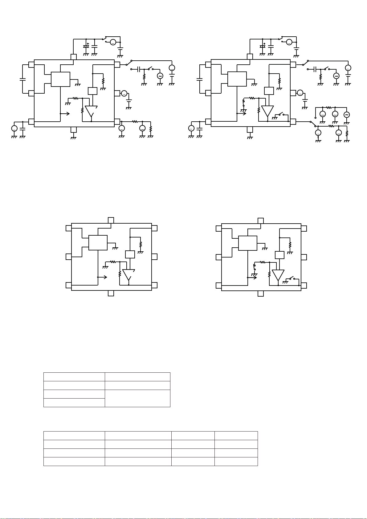
ͶDescription of Operation
! 1) Principles of output coupling capacitorless video drivers
Single-supply amplifier
VCC
1000ԜF
1/2 VCC bias
Output capacitor required since DC
voltage is occurring at output pin
75ǡ
75ǡ
Dual-supply amplifier
VCC
-VCC
Output capacitor not required since
DC voltage does not occur at output
pin
75ǡ
75ǡ
Fig.3 Fig.4
For an amplifier operated from a single power supply (single-supply), since the operating point has a potential of
approximately 1/2 Vcc, a coupling capacitor is required for preventing direct current in the output. Moreover, since the
load resistance is 150 (75 + 75 ) for the video driver, the capacity of the coupling capacitor must be on the order of
1000 μF if you take into account the low band passband. (Fig.3)
For an amplifier operated from dual power supplies (+ supply), since the operating point can be at GND level, a coupling
capacitor for preventing output of direct current is not needed.
Moreover, since a coupling capacitor is not needed, in principle, there is no lowering of the low band characteristic at the
output stage. (Fig.4)
2) Occurrence of negative voltage due to charge pump circuit
A charge pump, as shown in Fig. 5, consists of a pair of switches (SW1, SW2) and a pair of capacitors (flying capacitor,
anchor capacitor). Switching the pair of switches as shown in Fig. 5 causes a negative voltage to occur by shifting the
charge in the flying capacitor to the anchor capacitor as in a bucket relay.
In this IC, by applying a voltage of +3 V, a negative voltage of approximately -2.8 V is obtained.
5/16
V
V
cc +3V
SW1 SW2
Charge current
+
㧙
Flying capaci tor
Anchor
Capacitor
Vcc +3 V
Charge current
SW1
+
Charge current
Flying capaci tor
SW2
㧙
-
Vcc occurs
㧙
Anchor Capacitor
+
cc +3V
Charging mode
㧙
+
Charge shi fting mode
㧙
+
+
occurs
㧙
-Vcc
Fig.5 Principles of Charge Pump Circuit
3) Configuration of BH769xxGU and BH76706GU
As shown in Fig. 6, a BH769xxGU or BH76706GU is a dual-supply amplifier and charge pump circuit integrated in one IC.
Accordingly, while there is +3 V single-supply operation, since a dual-supply operation amplifier is used, an output
coupling capacitor is not needed.
1ǴF
150k
AMP
VCC
VCC
75ǡ
75ǡ
Dual-supply amplifier
1-chip integration
Although single-supply,
output capacitor is not needed.
Charge pump
-VCC
1ǴF
Charge pump
1ǴF
Fig.6 Configuration Diagram of BH769xxGU or BH76706GU
4) Input pin format and sag characteristic
While a BH769xxGU or BH76706GU is a low voltage operation video driver, since it has a large dynamic range of
approximately 5.2 Vpp, a resistance termination method that is compatible regardless of signal form (termination by 150
k) is used, and not a clamp method that is an input method exclusively for video signals.
Therefore, since a BH769xxGU or BH76706GU operates normally even if there is no synchronization signal in the input
signal, it is compatible with not only normal video signals but also chroma signals and R.G.B. signals and has a wide
application range.
Moreover, concerning sag (lowering of low band frequency) that occurs at the input pin and becomes a problem for the
resistance termination method, since the input termination resistor is a high 150 k, even if it is combined with a small
capacity input capacitor, a sag characteristic that is not a problem in actual use is obtained.
In evaluating the sag characteristic, it is recommended that you use an H-bar signal in which sag readily stands out. (Fig.
8 to Fig. 10)
6/16

Input capacitor and input impedance cutoff
frequency is the same as when output capacitor in
generic 75 driver is made 1000 μF.
(Input pin time constant) (Output pin time constant)
1 μF x 150 kȍ = 1000 μF x 150 ȍ
a)! Video signal without sag (TG-7/1 output, H-bar)
Sag is determined
by input capacitor
and input resistor
only.
Fig. 7
Fig. 8
1ԜF
150k
75Ԉ+75Ԉ=150Ԉ
Sag occurs
TV screen output image of
H-bar signal
b)! BH769xxGU or BH76706GU output (Input = 1.0 μF, TG-7/1 output, H-bar)
c)! 1000 μF + 150 sag waveform (TG-7/1 output, H-bar)
Fig. 9
TG-7/1
Fig. 10
1ԜF
150k
BH769xxGUBH76706GU
Nearly identical sag
Monitor
75Ԉ
1000Ԝ
TG-7/1
Monitor
75Ԉ
㪝㩷
75Ԉ
75Ԉ
7/16

ͶApplication Circuit Example
A
㪚㪶㪧㪣㪬㪪
㪚㪈㪔㪈㪅㪇㫌㪝 㪚㪈㪔㪈㪅㪇㫌㪝
㪚㪶㪤㪠㪥㪬㪪
㪥㪭㪚㪚
㪚㪉㪔㪈㪅㪇㫌㪝
t playback (Active mode)
㪉㪅㪌䌾㪊㪅㪋㪌㪭
㪭㪺㪺
㪘㪉㩷
㪘㪈㩷
㪚㪟㪘㪩㪞㪜㩷
㪧㪬㪤㪧
㪙㪈㩷
㪪㪮㪉㩷
㪚㪈㩷
㪥㪭㪚㪚
㪚㪉㩷
㪞㪥㪛
㪚㪋㪔㪊㪅㪊㫌㪝
㪣㪧㪝
㪍㪆㪐㪆㪈㪉㪆㪈㪍㪅㪌㪻㪙
㪈㪌㪇㫂
㪪㪮㪈㩷
㪚㪊㪔㪈㪅㪇㫌㪝 㪚㪊㪔㪈㪅㪇㫌㪝
㪭㪠㪥
㪘㪊㩷
㪭㪠㪛㪜㪦 㪠㪥
㪪㪫㪙㪰
㪙㪊㩷
Video
㪚㪊㩷
㪭㪦㪬㪫
㪭㪠㪛㪜㪦 㩷㪦㪬㪫
䌒㪉䋽㪎㪌㱅
monitor
Recording (Input mode) BH76706GU only
㪉㪅㪌䌾㪊㪅㪋㪌㪭
㪭㪺㪺㩷
㪚㪟㪘㪩㪞㪜
㪧㪬㪤㪧
㪥㪭㪚㪚
㪘㪉㩷
㪪㪮㪉㩷
㪚㪉㩷
㪣㪧㪝
㪍㪻㪙
㪞㪥㪛㩷
㪚㪉㪔㪈㪅㪇㫌㪝
㪚㪶㪧㪣㪬㪪
㪘㪈㩷
㪙㪈㩷
㪚㪶㪤㪠㪥㪬㪪
㪥㪭㪚㪚
㪚㪈㩷
㪚㪋㪔㪊㪅㪊㫌㪝
㪈㪌㪇㫂
㪪㪮㪈㩷
㪭㪦㪬㪫
㪭㪠㪥
㪘㪊㩷
㪪㪫㪙㪰
㪙㪊㩷
㪚㪊㩷
㪭㪠㪛㪜㪦 㪠㪥
䌒㪉䋽㪎㪌㱅
㪭㪠㪛㪜㪦 㩷㪠㪥
㪎㪌㱅
ͰSW1 and SW2 are built-in BH76706GU only!!!!!! See page 3/16 for STBY pin logic in each mode
Fig.11
We are confident in recommending the above application circuit example, but we ask that
you carefully check not just the static characteristics but also transient characteristics of this
circuit before using it.
ͶCaution on use
1.! Wiring from the decoupling capacitor C4 to the IC should be kept as short as possible.
Moreover, this capacitor's capacitance value may have ripple effects on the IC, and may affect the S-N ratio for signals, so
we recommend using as large a decoupling capacitor as possible. (Recommended C4: 3.3 F, B characteristics, 6.3 V
or higher maximum voltage)
Make mount board patterns follow the layout example shown on page 10 as closely as possible.
2.! Capacitors to use
In view of the temperature characteristics, etc., we recommend a ceramic capacitor with B characteristics.
3. The NVCC (C1 pin) terminal generates a voltage that is used within the IC, so it should never be connected to a load
unless absolutely necessary. Moreover, this capacitor (C2) has a large capacitance value but very little negative voltage
ripple.
(Recommended C2: 1.0 μF, B characteristic, 6.3 V or higher maximum voltage)
4. Capacitors C1 and C4 should be placed as close as possible to the IC. If the wiring to the capacitor is too long, it can lead
to intrusion of switching noise. (Recommended C1: 1.0 F, B characteristics, 6.3 V or higher maximum voltage)
5. The HPF consists of input coupling capacitor C3 and 150 kȍ of internal input impedance.
Be sure to check for video signal sag before determining the C3 value.
The cut-off frequency fc can be calculated using the following formula.
fc = 1/(2ԠC3150kԈ) (Recommended C3: 1.0 μF, B characteristic, 6.3 V or higher maximum voltage)
6. The output resistor R2 should be placed close to the IC.
7. If the IC is mounted in the wrong direction, there is a risk of damage due to problems such as inverting VCC and GND.
Be careful when mounting it.
8
. A large current transition occurs in the power supply pin when the charge pump circuit is switched. If this affects other ICs
(via the power supply line), insert a resistor (approximately 10 ȍ) in the VCC line to improve the power supply's ripple
effects. Although inserting a 10 ȍ resistor lowers the voltage by about 0.2 V, this IC has a wide margin for low-voltage
operation, so dynamic range problems or other problems should not occur. (See Figures 12 to 14.)
8/16

1. Current ripple due to charge pump
circuit affects power supply Vcc pin
1uF 3.3uF
DAC
1VJGT
Fig.12! Effects of Charge Pump Circuit Current Ripple on External Circuit
1) Decoupling capacitor only
Fig.13
2) Decoupling capacitor + 10 ȍ resistor
2. Current ripple affects
DAC or other
QT
1uF
Fig.14
Vcc
Ԉ
10
Vcc pin
V
IN
VIDEO
AMP
Ԉ
150k
V
OUT
-Vcc
75
Ԉ
75
Ԉ
Chrarge Pump
1uF
Waveform of current between
power supply and capacitor (A)
10 mA/div
Waveform of current between
capacitor and IC (B)
10 mA/div
A
Waveform of current between
power supply and capacitor (A)
10 mA/div
Waveform of current between
resistor and capacitor (B)
10 mA/div
Waveform of current between
capacitor and IC (C)
10 mA/div
A
C
Vcc
B
Vcc
A
10
Ԉ
A
A
B
Vcc
A
Vcc
A
9/16

ͶEvaluation Board Pattern Diagram (Double-sided, 2 layers)
Parts List
Symbol Function Recommended Value Remarks
Fig.15
Layer 1 wiring + Silkscreen
legend
Layer 2 wiring
Solder pattern
C1 Flying capacitor
C2 Tank capacitor
C3 Input coupling capacitor
C4 Decoupling capacitor
R1 Input termination resistor
R2 Output resistor
R3 Output termination resistor
Input connector BNC
Output connector RCA (Pin jack)
1ԜF
1ԜF
1ԜF
3.3ԜF
75Ԉ
75Ԉ
75Ԉ
B characteristic recommended
B characteristic recommended
B characteristic recommended
B characteristic recommended
Needed when connected to video signal measurement set
Not needed when connected to TV or video signal
measurement set
10/16

ͶReference Data
BH76906GU
㪊㪇
Ta= 2 5
BH76906GU
㪉㪌
VCC=3V
BH76906GU
㪇㪅㪋
Ta= 2 5
㪉㪌
㪉㪇
㪈㪌
㪈㪇
CIRCUIT CURRENT [mA]
㪌
㪇
㪇㪈㪉㪊㪋
POWER SUPPLY VOLTAGE [V]
Fig. 16 Circuit Current vs Supply Voltage
BH76906GU
㪇㪅㪋
㪇㪅㪊
㪇㪅㪉
㪇㪅㪈
STANDBY CURRENT [uA]
㪇
㪄㪇㪅㪈
㪄㪏㪇 㪄㪋㪇 㪇 㪋㪇 㪏㪇 㪈㪉㪇
TEMPERATURE []
VCC=3V
Fig. 19 Standby Circuit Current
vs Ambient Temperature
㪉㪇
㪈㪌
㪈㪇
CIRCUIT CURRENT [mA]
㪌
㪄㪏㪇 㪄㪋㪇 㪇 㪋㪇 㪏㪇 㪈㪉㪇
TEMPERATURE []
Fig. 17 Circuit Current
vs Ambient Temperature
BH76706GU
㪉㪇㪇
㪈㪌㪇
㪈㪇㪇
㪌㪇
CIRCUIT CURRENT [ǴA]
㪇
㪉㪉㪅㪌㪊㪊㪅㪌㪋
POWER SUPPLY VOLTAGE
Ta= 2 5
Fig. 20 GND Mode Circuit Current
vs Supply Voltage
㪇㪅㪊
㪇㪅㪉
㪇㪅㪈
㪇
STANDBY CURRENT [uA]
㪄㪇㪅㪈
㪉㪉㪅㪌㪊㪊㪅㪌㪋
POWER SUPPLY VOLTAGE [V]
Fig. 18 Standby Circuit Current
vs Supply Voltage
BH76706GU
㪉㪇㪇
㪈㪌㪇
㪈㪇㪇
㪌㪇
CIRCUIT CURRENT [ǴA]
㪇
㪄㪏㪇 㪄㪋㪇 㪇 㪋㪇 㪏㪇 㪈㪉㪇
TEMPERATURE []
VCC=3V
Fig. 21 GND Mode Circuit Current
vs Ambient Temperature
BH76906GU
㪌
㪇
㪄㪌
㪄㪈㪇
VOUT DC OFFSET [mV]
㪄㪈㪌
㪉 㪉㪅㪌 㪊 㪊㪅㪌 㪋
POWER SUPPLY VOLTAGE [V]
Ta= 2 5
Fig. 22 VOUT Pin Output DC Offset
vs Supply Voltage
BH76706GU
㪈㪇
㪇
㪄㪈㪇
㪄㪉㪇
㪄㪊㪇
㪄㪋㪇
㪄㪌㪇
VOLTAGE GAIN [dB]
㪄㪍㪇
㪄㪎㪇
㪄㪏㪇
㪈㪅㪜㪂㪇㪍 㪈㪅㪜㪂㪇㪎 㪈㪅㪜㪂㪇㪏
FREQUENCY [Hz]
VCC=3V Ta=25
Fig. 25 Frequency Characteristic
BH76906GU
㪌
㪇
㪄㪌
㪄㪈㪇
VOUT DC OFFSET [mV]
㪄㪈㪌
㪄㪏㪇 㪄㪋㪇 㪇 㪋㪇 㪏㪇 㪈㪉㪇
TEMPERATURE []
VCC=3V
Fig. 23 VOUT Pin Output DC Offset
vs Ambient Temperature
BH76906GU
㪍㪅㪉
㪍㪅㪈
㪍
VOLTAGE GAIN [dB]
㪌㪅㪐
㪌㪅㪏
㪉㪉㪅㪌㪊㪊㪅㪌㪋
POWER SUPPLY VOLTAGE [V]
Ta= 2 5
Fig. 26 Voltage Gain
vs Supply Voltage
BH76906GU
㪈㪇
㪇
㪄㪈㪇
㪄㪉㪇
㪄㪊㪇
㪄㪋㪇
㪄㪌㪇
VOLTAGE GAIN [dB]
㪄㪍㪇
㪄㪎㪇
㪄㪏㪇
㪈㪅㪜㪂㪇㪍 㪈㪅㪜㪂㪇㪎 㪈㪅㪜㪂㪇㪏
FREQUENCY [Hz]
VCC=3V Ta=25
Fig. 24 Frequency Characteristic
BH76906GU
㪍㪅㪉
㪍㪅㪈
㪍
VOLTAGE GAIN [dB]
㪌㪅㪐
㪌㪅㪏
㪄㪏㪇 㪄㪋㪇 㪇 㪋㪇 㪏㪇 㪈㪉㪇
TEMPERATURE []
VCC=3V
Fig. 27 Voltage Gain
vs Ambient Temperature
11/16

㪇㪅㪋
BH76906GU
Ta= 2 5
㪇㪅㪉
㪇
f=4.5MHz/100kHz
㪄㪇㪅㪉
FREQUENCY RESPONSE1:Gf1[dB]
㪄㪇㪅㪋
㪉㪉㪅㪌㪊㪊㪅㪌㪋
Fig. 28 Frequency Characteristic 1
POWER SUPPLY VOLTAGE
vs Supply Voltage
BH76906GU
㪄㪈
㪄㪉
VCC=3V
㪄㪊
㪄㪋
FREQUENCY RESPONSE2:Gf2[dB]
㪄㪌
㪄㪏㪇 㪄㪋㪇 㪇 㪋㪇 㪏㪇 㪈㪉㪇
TEMPERATURE []
Fig. 31 Frequency Characteristic 2
vs Ambient Temperature
f=8MHz/100kHz
BH76906GU
㪇㪅㪋
㪇㪅㪉
㪇
㪄㪇㪅㪉
FREQUENCY RESPONSE1:Gf1[dB]
㪄㪇㪅㪋
㪄㪏㪇 㪄㪋㪇 㪇 㪋㪇 㪏㪇 㪈㪉㪇
f=4.5MHz/100kHz
TEMPARATURE []
VCC=3V
Fig. 29 Frequency Characteristic 1
vs Ambient Temperature
BH76906GU
㪄㪉㪇
㪄㪉㪌
㪄㪊㪇
FREQUENCY RESPONSE3:Gf3[dB]
㪄㪊㪌
㪉㪉㪅㪌㪊㪊㪅㪌㪋
POWER SUPPLY VOLTAGE [V]
f=18MHz/100kHz
f=18MHz/100kHz
Ta= 2 5
Fig.32 Frequency Characteristic 3
vs Supply Voltage
BH76906GU
㪄㪈
㪄㪉
㪄㪊
㪄㪋
FREQUENCY RESPONSE2:Gf2[dB]
㪄㪌
㪉㪉㪅㪌㪊㪊㪅㪌㪋
POWER SUPPLY VOLTAGE [V]
Ta= 2 5
f=8MHz/100kHz
Fig. 30 Frequency Characteristic 2
vs Supply Voltage
BH76906GU
㪄㪉㪇
f=18MHz/100kHz
㪄㪉㪌
㪄㪊㪇
FREQUENCY RESPONSE3:Gf3[dB]
㪄㪊㪌
㪄㪏㪇 㪄㪋㪇 㪇 㪋㪇 㪏㪇 㪈㪉㪇
TEMPERATURE []
VCC=3V
Fig.33 Frequency Characteristic 3
vs Ambient Temperature
BH76906GU
㪄㪊㪌
㪄㪋㪇
㪄㪋㪌
FREQUENCY RESPONSE4:Gf4[dB]
㪄㪌㪇
㪉㪉㪅㪌㪊㪊㪅㪌㪋
POWER SUPPLY VOLTAGE [V]
Ta= 2 5
f=23.5MHz/100k
Fig. 34 Frequency Characteristic4
vs Supply Voltage
MAX OUTPUT VOLTAGE [Vpp]
BH76906GU
㪍
㪌㪅㪏
㪌㪅㪍
㪌㪅㪋
㪌㪅㪉
VCC=3V
BH76906GU
㪄㪊㪌
㪄㪋㪇
㪄㪋㪌
FREQUENCY RESPONSE4:Gf4[dB]
㪄㪌㪇
㪄㪏㪇 㪄㪋㪇 㪇 㪋㪇 㪏㪇 㪈㪉㪇
TEMPERATURE []
f=23.5MHz/100k
VCC=3V
Fig. 35 Frequency Characteristic 4
vs Ambient Temperature
VCC=3V!!Ta =2 5
OUTPUT DC VOLTAGE [V]
3
2
1
6dB
0
9dB
12dB
16.5dB
-1
-2
BH76906GU
㪎
㪍
㪌
㪋
MAX OUTPUT VOLTAGE [Vpp]
㪊
㪉㪉㪅㪌㪊㪊㪅㪌㪋
POWER SUPPLY VOLTAGE [V]
Ta= 2 5
Fig. 36 Max. Output Level
vs Supply Voltage
㪌
㪄㪏㪇 㪄㪋㪇 㪇 㪋㪇 㪏㪇 㪈㪉㪇
TEMPARATURE []
Fig. 37 Max. Output Level
vs Ambient Temperature
-3
-1.5 - 1.0 - 0.5 0.0 0.5 1.0 1.5
INPUT DC VOLTAGE [V]
Fig. 38 DC I/O Characteristic
12/16

CHARGEPUMP OSC FREQUENCY [KHz]
BH76906GU
㪉㪊㪇
㪉㪉㪌
㪉㪉㪇
㪉㪈㪌
㪉㪈㪇
㪉㪇㪌
㪉㪇㪇
㪉㪉㪅㪌㪊㪊㪅㪌㪋
POWER SUPPLY VOLTAGE [V]
Fig. 39 Charge Pump Oscillation Frequency
vs Supply Voltage
Ta= 2 5
BH76906GU
㪉㪊㪇
㪉㪉㪌
㪉㪉㪇
㪉㪈㪌
㪉㪈㪇
CHARGEPUMP OSC FREQUENCY [KHz]
㪉㪇㪌
㪄㪏㪇 㪄㪋㪇 㪇 㪋㪇 㪏㪇 㪈㪉㪇
TEMPERATURE []
VCC=3V
Fig. 40 Charge Pump Oscillation Frequency
vs Ambient Temperature
BH76906GU
㪄㪈
㪄㪈㪅㪌
㪄㪉
㪄㪉㪅㪌
㪄㪊
㪄㪊㪅㪌
CHARGEPUMP OUTPUT VOLTAGE [V]
㪄㪋
㪉㪉㪅㪌㪊㪊㪅㪌㪋
POWER SUPPLY VOLTAGE [V]
Ta= 2 5
Fig. 41 Charge Pump Output Voltage
vs Supply Voltage
BH76912GU
㪈㪅㪉
㪈㪅㪈
㪈
㪇㪅㪐
DIFFERENTIAL PHASE [Deg]
Ta= 2 5
㪄㪈㪅㪇
BH76906GU
VCC=3V Ta=25
㪄㪈㪅㪌
㪄㪉㪅㪇
㪄㪉㪅㪌
CHARGEPUMP OUTPUT VOLTAGE [V]
㪄㪊㪅㪇
㪇㪅㪇 㪈㪇㪅㪇 㪉㪇㪅㪇 㪊㪇㪅㪇 㪋㪇㪅㪇
LOAD CURRENT [mA]
Fig. 42 Charge Pump Load Regulation
!!!!!
BH76912GU
㪈㪅㪉
㪈㪅㪈
㪈
㪇㪅㪐
DIFFERENTIAL PHASE [Deg]
VCC=3V
㪇㪅㪏
㪉㪉㪅㪌㪊㪊㪅㪌㪋
POWER SUPPLY VOLTAGE [V]
Fig. 43 Differential Phase
vs Supply Voltage
BH76912GU BH76912GU
㪇㪅㪏
㪇㪅㪍
㪇㪅㪋
㪇㪅㪉
DIFFERENTIAL GAIN [%]
㪇
㪉㪉㪅㪌㪊㪊㪅㪌㪋
POWER SUPPLY VOLTAGE [V]
Ta= 2 5
Fig. 45 Differential Gain
vs Supply Voltage
13/16
㪇㪅㪏
㪄㪏㪇 㪄㪋㪇 㪇 㪋㪇 㪏㪇 㪈㪉㪇
TEMPERATURE []
Fig. 44 Differential Phase
vs Ambient Temperature
㪇㪅㪏
㪇㪅㪍
㪇㪅㪋
㪇㪅㪉
DIFFERENTIAL GAIN [%]
㪇
㪄㪏㪇 㪄㪋㪇 㪇 㪋㪇 㪏㪇 㪈㪉㪇
TEMPERATURE []
Fig. 46 Differential Gain
vs Ambient Temperature
VCC=3V

BH76906GU BH76906GU
㪎㪐
Ta= 2 5
㪎㪐
VCC=3V
㪎㪏㪅㪌
㪎㪏㪅㪌
㪎㪏
Y S/N [dB]
㪎㪎㪅㪌
㪎㪎
㪉 㪉㪅㪌 㪊 㪊㪅㪌 㪋
POWER SUPPLY VOLTAGE [V]
Fig. 47 Y S/N vs Supply Voltage
BH76906GU
㪏㪇
㪎㪏
㪎㪍
Ta= 2 5
㪎㪋
CHROMA S/N (AM) [dB]
㪎㪉
㪎㪇
㪉 㪉㪅㪌 㪊 㪊㪅㪌 㪋
POWER SUPPLY VOLTAGE [V]
Fig. 49 C AM S/N vs Supply Voltage
㪎㪏
Y S/N [dB]
㪎㪎㪅㪌
㪎㪎
㪄㪏㪇 㪄㪋㪇 㪇 㪋㪇 㪏㪇 㪈㪉㪇
TEMPERATURE []
Fig.48 Y S/N vs Ambient Temperature
BH76906GU
㪏㪇
㪎㪏
㪎㪍
㪎㪋
CHROMA S/N (AM) [dB]
㪎㪉
㪎㪇
㪄㪏㪇 㪄㪋㪇 㪇 㪋㪇 㪏㪇 㪈㪉㪇
TEMPERATURE []
VCC=3V
Fig. 50 C AM S/N vs Ambient Temperature
BH76906GU
㪎㪇
Ta= 2 5
㪎㪇
BH76906GU
VCC=3V
㪍㪏
㪍㪍
㪍㪏
㪍㪍
㪍㪋
CHROMA S/N (PM) [dB]
㪍㪉
㪍㪇
㪉㪉㪅㪌 㪊㪊㪅㪌㪋
POWER SUPPLY VOLTAGE [V]
Fig. 51 C PM S/N vs Supply Voltage
㪈㪏㪇
BH76906GU
㪈㪍㪌
㪈㪌㪇
㪈㪊㪌
INPUT IMPEDANCE [kԈ]
㪈㪉㪇
㪉㪉㪅㪌㪊㪊㪅㪌㪋
POWER SUPPLY VOLTAGE [V]
Fig. 53 Input Impedance vs Supply Voltage
Ta= 2 5
14/16
㪍㪋
CHROMA S/N (PM) [dB]
㪍㪉
㪍㪇
㪄㪏㪇 㪄㪋㪇 㪇 㪋㪇 㪏㪇 㪈㪉㪇
TEMPERATURE []
Fig. 52 C PM S/N vs Ambient Temperature
㪈㪍㪌
㪈㪌㪇
㪈㪊㪌
INPUT IMPEDANCE [kԈ]
㪈㪉㪇
BH76906GU
㪄㪏㪇 㪄㪋㪇 㪇 㪋㪇 㪏㪇 㪈㪉㪇
TEMPERATURE []
VCC=3V
Fig. 54 Input Impedance vs Ambient Temperature

BH76906GU
㪉㪇
㪈㪍
㪈㪉
VCC=3V Ta=25
㪏
㪋
CIRCUIT CURRENT [mA]
㪇
㪇㪅㪇 㪇㪅㪌 㪈㪅㪇 㪈㪅㪌 㪉㪅㪇 㪉㪅㪌 㪊㪅㪇
CTL TERMINAL VOLTAGE [V]
Fig. 55 Control Pin Characteristic
BH76706GU
㪉㪇
㪈㪍
㪈㪉
㪏
㪋
CIRCUIT CURRENT [mA]
㪇
㪇 㪇㪅㪌 㪈 㪈㪅㪌 㪉 㪉㪅㪌 㪊
CTL TERMINAL VOLTAGE [V]
Fig. 56 Control Pin Characteristic
VCC=3V Ta=25
㪌
BH76706GU
Ta= 2 5
BH76706GU
㪌
VCC=3V
㪋
㪋
㪊
㪊
㪉
ON RESISTANCE [Ԉ]
㪈
㪉㪉㪅㪌 㪊㪊㪅㪌㪋
POWER SUPPLY VOLTAGE [V]
Fig. 57! Output Pin Shunt Switch On Resistance
vs Supply Voltage
㪉
ON RESISTANCE [Ԉ]
㪈
㪄㪏㪇 㪄㪋㪇 㪇 㪋㪇 㪏㪇 㪈㪉㪇
POWER SUPPLY VOLTAGE [V]
Fig. 58! Output Pin Shunt Switch On Resistance
vs Ambient Temperature
Ͷ Performing separate electrostatic damage countermeasures
When adding an externally attached electrostatic countermeasure element to the output pin, connect a varistor in the
position shown in Fig. 59 (if connected directly to the output pin, the IC could oscillate depending on the capacity of the
varistor). For this IC, since the output waveform is GND-referenced and swings positive and negative, a normal Zener
diode cannot be used.
ESD or surge
VOUT
75Ԉ
75Ԉ
Fig.59 Using Externally Attached Varistor
15/16

ͶSelection of order type
VCSP85H1
B
H
7 6
Part. No.
BH76906GU
BH76909GU
BH76912GU
BH76916GU
BH76706GU
9 0
Tape
Quantit
Direction
of feed
1234 1234 1234 1234 1234 1234
6
Embossed carrier tape
3000pcs
E2
(The direction is the 1pin of product is at the upper left when you hold
reel on the left hand and you pull out the tape on the right hand)
G
U
E 2
Tape and Reel information
Reel
When you order , please order in times the amount of package quantity.
1pin
Direction of feed
Catalog No.06T216A '06.11 ROHM C 1600 TSU

Appendix
Notes
No technical content pages of this document may be reproduced in any form or transmitted by any
means without prior permission of ROHM CO.,LTD.
The contents described herein are subject to change without notice. The specifications for the
product described in this document are for reference only. Upon actual use, therefore, please request
that specifications to be separately delivered.
Application circuit diagrams and circuit constants contained herein are shown as examples of standard
use and operation. Please pay careful attention to the peripheral conditions when designing circuits
and deciding upon circuit constants in the set.
Any data, including, but not limited to application circuit diagrams information, described herein
are intended only as illustrations of such devices and not as the specifications for such devices. ROHM
CO.,LTD. disclaims any warranty that any use of such devices shall be free from infringement of any
third party's intellectual property rights or other proprietary rights, and further, assumes no liability of
whatsoever nature in the event of any such infringement, or arising from or connected with or related
to the use of such devices.
Upon the sale of any such devices, other than for buyer's right to use such devices itself, resell or
otherwise dispose of the same, no express or implied right or license to practice or commercially
exploit any intellectual property rights or other proprietary rights owned or controlled by
ROHM CO., LTD. is granted to any such buyer.
Products listed in this document are no antiradiation design.
The products listed in this document are designed to be used with ordinary electronic equipment or devices
(such as audio visual equipment, office-automation equipment, communications devices, electrical
appliances and electronic toys).
Should you intend to use these products with equipment or devices which require an extremely high level
of reliability and the malfunction of which would directly endanger human life (such as medical
instruments, transportation equipment, aerospace machinery, nuclear-reactor controllers, fuel controllers
and other safety devices), please be sure to consult with our sales representative in advance.
It is our top priority to supply products with the utmost quality and reliability. However, there is always a chance
of failure due to unexpected factors. Therefore, please take into account the derating characteristics and allow
for sufficient safety features, such as extra margin, anti-flammability, and fail-safe measures when designing in
order to prevent possible accidents that may result in bodily harm or fire caused by component failure. ROHM
cannot be held responsible for any damages arising from the use of the products under conditions out of the
range of the specifications or due to non-compliance with the NOTES specified in this catalog.
Thank you for your accessing to ROHM product informations.
More detail product informations and catalogs are available, please contact your nearest sales office.
ROHM Customer Support System
www.rohm.com
THE AMERICAS / EUROPE / ASIA / JAPAN
Contact us : webmaster@ rohm.co. jp
Copyright © 2008 ROHM CO.,LTD.
21 Saiin Mizosaki-cho, Ukyo-ku, Kyoto 615-8585, Japan
TEL : +81-75-311-2121
FAX : +81-75-315-0172
Appendix1-Rev2.0
 Loading...