


High-performance Video Driver Series
Output Capacitor-less
Video Drivers
BH76806FVM, BH76809FVM, BH76812FVM, BH76816FVM
No.09064EAT02
●Description
The BH768xx series video drivers are the optimum solution for high density integration systems such as, digital still
cameras, mobile phones, and portable video devices. A built-in charge pump circuit eliminates the need for a large output
coupling capacitor. Features include: a built-in LPF, low-voltage (2.5 V) operation, and 0 µA current consumption during
standby mode.
●Features
1) Select from four video driver amp gain settings: 6 dB, 9 dB, 12 dB, and 16 dB
2) Large-output video driver with maximum output voltage of 5.2 Vpp.
Supports wide and low-voltage operation range.
3) No output coupling capacitor is needed, which makes for a more compact design
4) Built-in standby function sets circuit current to 0 µA (typ.) during standby mode
5) Clear image reproduction by on-chip 8-order 4.5-MH
6) Bias input method is used to support chroma, video, and RGB signals.
7) MSOP8 compact package
●Applications
Mobile telephones, DSCs (digital still cameras), DVCs (digital video cameras), portable game systems,
portable media players, etc.
●Line up matrix
Part No. Video driver amp gain Recommended input level
z LPF (Low Pass Filter)
BH76806FVM 6dB 1Vpp
BH76809FVM 9dB 0.7Vpp
BH76812FVM 12dB 0.5Vpp
BH76816FVM 16.5dB 0.3Vpp
Absolute maximum ratings (T
Parameter Symbol Ratings Unit
Supply voltage Vcc 3.55 V
Power dissipation Pd 470 mW
Operating temperature range Topr
Storage temperature range Tstg -55~+125 ℃
* Reduce by 4.7 mW/C over 25C, when mounted on a 70mm×70mm×1.6mm PCB board.
a=25℃)
-40~+85 ℃
www.rohm.com
1/16
© 2009 ROHM Co., Ltd. All rights reserved.
2009.03 - Rev.A

BH76806FVM, BH76809FVM, BH76812FVM, BH76816FVM
Operating range (Ta=25℃)
Parameter Symbol Min. TYP. Max. Unit
Supply voltage Vcc 2.5 3.0 3.45 V
Electrical characteristics (Unless otherwise noted, Typ.: T
a=25℃, VCC=3V)
Typical value
Parameter Symbol
BH76806
FVM
BH76809
FVM
BH76812
FVM
BH76816
Technical Note
Unit Conditions
FVM
Circuit current 1 I
Circuit current 2 I
Standby SW input current
High-Level
Standby switching voltage
High-Level
Standby Switching voltage
Low-Level
16 15 mA No signal
CC1
0.0 A Standby mode
CC2
I
45 A When 3.0 V is applied to 4pin
thH
V
1.2V min V standby OFF
thH
V
0.45Vmax V standby ON
thL
Voltage gain GV 6.0 9.0 12.0 16.5 dB Vo=100KHz, 1.0Vpp
Maximum output level Vomv 5.2 Vpp f=1KHz,THD=1%
Frequency characteristic 1 Gf1 -0.45 dB f=4.5MHz/100KHz
Frequency characteristic 2 Gf2 -3.0 dB f=8.0MHz/100KHz
Frequency characteristic 3 Gf3 -32 dB f=18MHz/100KHz
Frequency characteristic 4 Gf4 -51 dB f=23.5MHz/100KHz
Differential Gain DG 0.5 %
Differential Phase DP 1.0 deg
Vo=1.0Vp-p
Standard stair step signal
V
o=1.0Vp-p
Standard stair step signal
Band = 100 kHz to 6 MH
Y signal output S/N SNY +74 +73 +70 +70 dB
75 termination
100% chroma video signal
Band = 100~500KHz
C signal output S/N (AM) SNCA +77 +76 +75 +75 dB
75Ωtermination
100%chroma video signal
Band = 100~500KH
C signal output S/N (PM) SNCP +65 dB
75Ωtermination
100%chroma video signal
Output pin source current lextin 30 mA
±50
Output DC offset voltage Voff
max
4.5 V applied via 150 to
output pin
75 termination
mV
z
z
www.rohm.com
2/16
© 2009 ROHM Co., Ltd. All rights reserved.
2009.03 - Rev.A

BH76806FVM, BH76809FVM, BH76812FVM, BH76816FVM
Measurement circuit
1. 0u F
1
A
V2
(VCC)
OSC1
1
2
SW3
SW2
10u
50
0. 1u
V4
2
0. 1u
3
4
IN OUT
CHARGE PUMP
GND
6d B/9d B/
LPF
150K
12d B/1 6. 5d B
※ Test circuit is intended for shipment inspections, and differs from application circuit.
Fig. 1
Control pin settings
Parameter States Note
NVCC
Technical Note
8
7
6
5
4. 7u
1. 0u F
75
V
75
V
Block diagram
Standby(4pin)
C1
C1
VCC
VCC
Vin
Vin
STBY
STBY
H Active
L Standby
OPEN Standby
1
IN OUT
2
3
CHARGE PUMP
LPF
GND
NVC C
6dB/9dB/
12dB /1 6.5dB
8
7
6
C2
C2
NVCC
NVCC
GND
GN D
AMP
150K
4
5
Vout
Vout
Fig.2
www.rohm.com
3/16
© 2009 ROHM Co., Ltd. All rights reserved.
2009.03 - Rev.A

BH76806FVM, BH76809FVM, BH76812FVM, BH76816FVM
T
Pin descriptions
Pin
No.
1
Pin
name
C1
equivalent circuit
VCC
VCC
DC
voltage
+VCC
↑↓
0V
C1
GND
GND
NVCC
2 VCC
VCC
Technical Note
Functions
Flying capacitor "+" pin
See function description for pins 7
and 8
VCC Pin
3 VIN
4 STBY
5
VOUT
VCC
4.1k
4.1k
VIN
100
150K
NV
0V
Video signal input pin
Adaptive input signal
Composite video signal/
VIN
1μF
chroma signal/RGB signal, etc.
STBY
VCC
VCC
50K
250K
200K
VCC
VCC
GND
GND
VOU
VCC
to
0V
0V
ACTIVE/STANBY Switching Pin
1.2V~VCC
0V~0.45V
Terminal
Votage
( H )
( L )
MODE
ACTIVE
STANBY
Video signal output pin
VOUT
NVCC
NVCC
1K
75Ω
75Ω
150k
VCC
6 GND
GND
0V
GND Pin
NVCC
*1 The DC voltage in the figure is VCC = 3.0 V. These values are for reference only and are not guaranteed.
*2 These values are for reference only and are not guaranteed.
www.rohm.com
4/16
© 2009 ROHM Co., Ltd. All rights reserved.
2009.03 - Rev.A

BH76806FVM, BH76809FVM, BH76812FVM, BH76816FVM
Technical Note
●Pin descriptions
7 NVCC
VCC
GND
VCC
-VCC
C2
(-2.75V)
Flying capacitor “-”pin
(8pin)
C1
C2
NVC
Load voltage pins (7 pins)
NVC
8 C2
GND
VCC
VCC
NVCC
0V
↑↓
-VCC
(-2.75V)
*1 The DC voltage in the figure is VCC = 3.0 V. These values are for reference only and are not guaranteed.
*2 These values are for reference only and are not guaranteed.
Description of operations
1) Principles of video driver with no output coupling capacitor
Amp (Single power supply)
Amp (Dual power supply)
VCC
1/2VCC Bias
Fig.3 Fig.4
When the amplifier operates using single voltage power supply, the operating potential point is approximately 1/2 Vcc.
Therefore, a coupling capacitor is required to prevent DC output. For the video driver, the load resistance is 150 (75
+ 75 ). Therefore, the coupling capacitor should be about 1000 µF when a low bandwidth for transmission is considered.
(See Figure 3.)
When the amplifier operates using a dual (±) power supply, the operating point can be set at GND level, and therefore,
there is no need for a coupling capacitor to prevent DC output.
Since a coupling capacitor is not needed, there is no sagging of low-frequency characteristics in output stage. (See Figure
4.)
2) Generation of negative voltage by charge pump circuit
As is shown in Figure 5, the charge pump consists of a pair of switches (SW1 and SW2) and a pair of capacitors (flying
capacitor and load capacitor), generating a negative voltage. When +3 V is applied to this IC, approximately -2.83 V of
negative voltage is obtained.
Output capacitor is required due to DC
voltage at output pin
75Ω
1000μF
75Ω
VCC
-VCC
Output capacitor is not required since
DC voltage is not applied to output pin
75Ω
75Ω
VCC
0V
www.rohm.com
5/16
© 2009 ROHM Co., Ltd. All rights reserved.
2009.03 - Rev.A

BH76806FVM, BH76809FVM, BH76812FVM, BH76816FVM
ア
Technical Note
Vcc +3V
charge current
+
SW1 SW2
Flying capacitor
Vcc +3V
charge current
SW1 SW2
-
Load capacitor
+
-
charge current
Flying capacitor
-Vcc is generated
-
Load capacitor
+
Vcc +3V
charge current
+
-
charge transfer mode
-
+
+
-
-Vcc is generated
Fig. 5 Principles of Charge Pump Circuit
1) Configuration of BH768xxFVM Series
As is shown in Figure 6, in the BH768xxFVM Series, a dual power supply amplifier is integrated with a charge pump circuit
in the same IC. This enables operation using a + 3V single power supply while also using a dual power supply amplifier,
which eliminates the need for an output coupling capacitor.
1μF
AMP
VCC
Dual power supply amp
ンプ H768xxFVM
75Ω
150k
VCC
75Ω
Single chip
integration
Output capacitor not required
for single power supply either.
Charge Pump
-VCC
3.3μF
Charge pump
768xxFVM
1μF
Fig. 6 BH768xxFVM Configuration Diagram
2) Input terminal type and sag characteristics
BH768xxFVM Series devices provide both a low-voltage video driver and a large dynamic range (approximately 5.2 Vpp).
A resistance termination method (150 k termination) is used instead of the clamp method, which only supports video
signals, since it supports various signal types.
The BH768xxFVM series supports a wide range of devices such as, video signals, chroma signals, and RGB signals that
can operate normally even without a synchronization signal.
In addition, input terminating resistance (150 k) can use a small input capacitor without reducing the sag low-band
It is recommended to use a H-bar signal when evaluating sag characteristics, since it makes sag more noticeable. (See
Figures 7 to 10.)
www.rohm.com
6/16
© 2009 ROHM Co., Ltd. All rights reserved.
2009.03 - Rev.A

BH76806FVM, BH76809FVM, BH76812FVM, BH76816FVM
Technical Note
Cut-off frequency for input capacitor and input impedance is
the same as when the output capacitor is set at 1000 µF with
an ordinary 75 driver.
(Input terminal time constant) (Output terminal time constant)
a) Sag-free video signal (TG-7/1 output, H-bar)
b) BH768xxFVM output (input = 1.0 µF, TG-7/1 output, H-bar)
c) 1000 uF + 150 sag waveform (TG-7/1 output, H-bar)
1 F X 150 K = 1000 F X 150
Sag is determined
by input capacitor
and input
resistance only.
1μF
150k
Fig. 7
Fig. 8
TG-7/1
Fig. 9
Fig. 10
75Ω+75Ω=150Ω
Sag
H-bar signal's TV screen
output image
75Ω
Monitor
1μF
150k
BH768xxFVM
Nearly identical sag characteristics
75Ω
TG-7/1
Monitor
1000μF
75Ω
75Ω
75Ω
www.rohm.com
7/16
© 2009 ROHM Co., Ltd. All rights reserved.
2009.03 - Rev.A

BH76806FVM, BH76809FVM, BH76812FVM, BH76816FVM
Application circuit
1.0μF(C18)
Technical Note
1
OUT
6dB/9dB/
12dB/16.5dB
NVCC
150k
IN
CHARGE PUNP
LPF
GND
Fig. 11
※
10Ω(R2)
2
3.3μF
(C2)
VIDEO IN
1.0μF(C3)
L:Standby
High Active
Open Standby
Low Standby
3
4
※Although ROHM is confident that the example application circuit reflects the best possible
recommendations, be sure to verify circuit characteristics for your particular application.
8
7
6
75Ω(R5)
5
1.0μF(C7)
VIDEO OUT
www.rohm.com
8/16
© 2009 ROHM Co., Ltd. All rights reserved.
2009.03 - Rev.A

BH76806FVM, BH76809FVM, BH76812FVM, BH76816FVM
c
c
1.Effects of charge pump
circuit’s current ripple
Vcc
10Ω
1μF
DAC etc.
2.Current ripple affects DAC, etc.
1μF
V
IN
Vcc pin
VIDEO
AMP
150kΩ
Charge Pump
Fig. 12 Effect of Charge Pump Circuit's Current Ripple on External Circuit
1) Decoupling capacitor only
Current waveform (A) between single
power supply and capacitor
10mA/div
Current waveform (B)
between capacitor and IC
10mA/div
Fig.13
2) Decoupling capacitor + Resistance 10Ω
Current waveform (A) between single
power supply and capacitor
10mA/div
Current waveform (B)between single
power supply and capacitor
10mA/div
Current waveform (C)between single
power supply and capacitor
10mA/div
Fig.14
3.3μF
V
-Vcc
A
OUT
Technical Note
75Ω
75Ω
1μF
Vc
A
A
B
A
Vc c
Vc
10
Ω
A
C
Vc c
A
B
A
www.rohm.com
9/16
© 2009 ROHM Co., Ltd. All rights reserved.
2009.03 - Rev.A
BH76806FVM, BH76809FVM, BH76812FVM, BH76816FVM
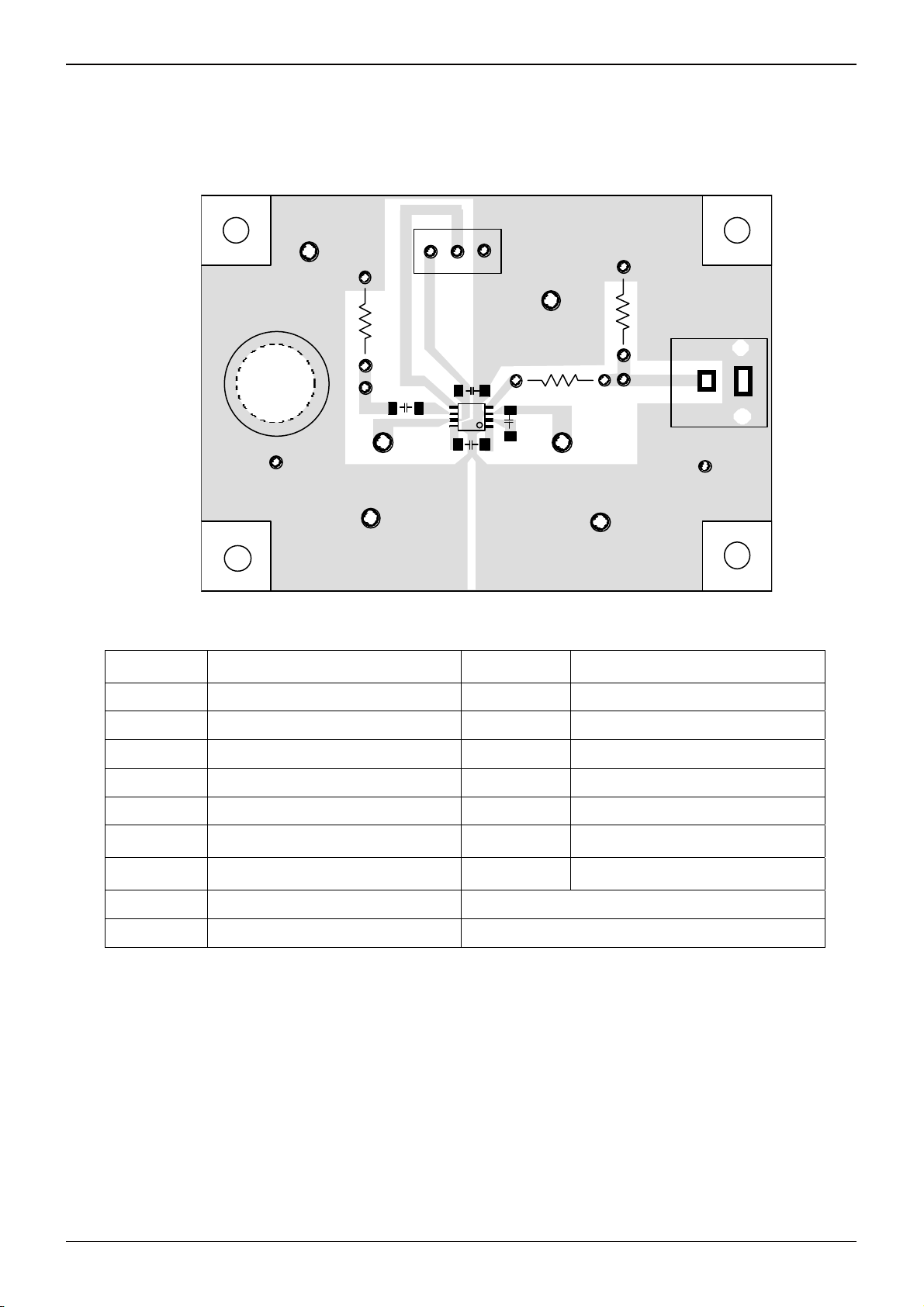
Pattern diagram of evaluation board
GND
STBY
ACT
VIN
R3
GND
C3
C4
R1
C2
GND
VCC
C1
GND
GND
ROHM BH76806/09/12/16FVM
List of external components
Fig. 15
Symbol Function
Recommended
value
C1 Flying capacitor 1μF B characteristics are recommended
C2 Tank capacitor
C3 Input coupling capacitor
1μF
1μF
Technical Note
R2
GND
B characteristics are recommended
B characteristics are recommended
VOUT
GND
Remark
C4 Decoupling capacitor 3.3μF B characteristics are recommended
R1 Output resistor
R2 Output terminating resistance 75Ω
R3 Input terminating resistance 75Ω
Input connector BNC
Output connector RCA (pin jack)
75Ω -
Not required when connecting to TV
or video signal test equipment.
Required when connecting to video
signal test equipment.
www.rohm.com
10/16
© 2009 ROHM Co., Ltd. All rights reserved.
2009.03 - Rev.A

BH76806FVM, BH76809FVM, BH76812FVM, BH76816FVM
Technical Note
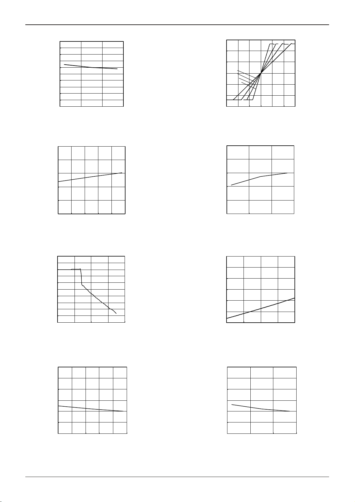
Reference data
BH76812FVM
30
25
20
15
10
CIRCUIT CURRENT [mA]
5
0
01234
POWER SUPPLY VOLTAGE [V]
Fig. 16 Circuit current vs. Supply voltage
BH76812FVM
20
18
16
14
12
CIRCUIT CURRENT [mA]
10
-50 0 50 100
TEMPERATURE [℃]
Fig. 18 Circuit current vs. Temperature
BH76812FVM
50
25
Ta= 2 5℃
VCC=3V
Ta= 2 5℃
BH76812FVM
1
0.8
0.6
0.4
0.2
STANDBY CURRENT [uA]
0
2.5 2.7 2.9 3.1 3.3 3.5
POWER SUPPLY VOLTAGE [V]
Ta= 2 5
℃
Fig. 17 Circuit Current (Standby) vs. Supply Voltage
STANDBY CURRENT [uA]
BH76812FVM
1
0.8
0.6
0.4
0.2
0
-50 0
TEMPERATURE [
VCC=3V
50 100
℃]
Fig. 19 Circuit Current (Standby) vs. Temperature
BH76812FVM
50
25
VCC=3V
0
-25
VOUT DC OFFSET [mV]
-50
2.5
2.7 2.9 3.1
POWER SUPPLY VOLTAGE [V]
Fig. 20 V
out DC offset voltage
3.3 3.5
vs. Supply voltage
VOLTAGE GAIN [dB]
BH76812FVM
5
-5
-15
-25
-35
-45
-55
-65
-75
0.1
VCC=3V Ta=25
1
FREQUENCY [MHz]
10
Fig. 22 Frequency characteristic
℃
100
0
-25
VOUT DC OFFSET [mV]
-50
-50 0 50 100
Fig. 21 V
TEMPERATURE [
out DC offset voltage
℃]
vs. Temperature
BH76812FVM
12.5
12.4
12.3
12.2
12.1
12
11.9
11.8
VOLTAGE GAIN [dB]
11.7
11.6
11.5
2.5 2.7 2.9 3.1 3.3 3.5
POWER SUPPLY VOLTAGE [V]
Ta= 2 5
℃
Fig. 23 Voltage gain vs. Supply voltage
www.rohm.com
11/16
© 2009 ROHM Co., Ltd. All rights reserved.
2009.03 - Rev.A

BH76806FVM, BH76809FVM, BH76812FVM, BH76816FVM
Technical Note
BH76812FVM
12.5
12.4
12.3
12.2
12.1
12
11.9
11.8
VOLTAGE GAIN [dB]
11.7
11.6
11.5
-50 0 50 100
TEMPERATURE [
Fig. 24 Voltage gain vs. Temperature
BH76812FVM
1
0.8
0.6
0.4
0.2
0
-0.2
-0.4
-0.6
-0.8
FREQUENCY RESPONSE1:Gf1[dB]
-1
-50 0 50 100
f=4. 5MHz/100kHz
TEMPERATURE[℃]
VCC=3V
℃]
VCC=3V
Fig. 26 Frequency response 1 vs. Temperature
BH76812FVM
0
-1
-2
-3
-4
-5
FREQUENCY RESPONSE2:Gf2[dB]
-6
-50 0 50 100
TEMPERATURE [
VCC=3V
f=8MHz/100kHz
℃]
BH76812FVM
1
0.8
0.6
0.4
0.2
0
-0.2
-0.4
-0.6
-0.8
FREQENCY RESPONSE1:Gf1[dB]
-1
2.5 2.7 2.9 3.1 3.3 3.5
POWER SUPPLY VOLTAGE:Vcc[V]
f=4. 5MHz/100kHz
Ta= 2 5
℃
Fig. 25 Frequency response 1 vs. Supply voltage
BH76812FVM
0
-1
-2
-3
-4
-5
FREQUENCY RESPONSE2:Gf2[dB]
-6
2.5 2.7 2.9 3.1 3.3 3.5
POWER SUPPLY VOLTAGE: Vcc [V]
Ta= 2 5℃
f=8MHz/100kHz
Fig. 27 Frequency response 2 vs. Supply voltage
BH76812FVM
-40
-45
-50
-55
-60
-65
FREQUENCY RESPONSE4:Gf4[dB]
-70
2.5 2.7 2.9 3.1 3.3 3.5
POWER SUPPLY VOLTAGE:Vcc[V]
f=23.5MHz/100kHz
Ta= 2 5
℃
Fig. 28 Frequency response 2 vs. Temperature
BH76812FVM
-40
-45
-50
-55
-60
-65
FREQUENCY RESPONSE4:Gf4[dB]
-70
-50 0 50 100
TEMPERATURE [℃]
f=23.5MHz/100kHz
TEMPERATURE [Deg]
VCC=3V
Fig. 30 Frequency response 4 vs. Temperature
www.rohm.com
12/16
© 2009 ROHM Co., Ltd. All rights reserved.
Fig.29 Frequency response 4 vs. Supply voltage
BH76812FVM
7
6
5
4
3
2
1
MAX OUTPUT VOLTAGE [Vpp]
0
2.52.72.93.13.33.5
POWER SUPPLY VOLTAGE [V]
Ta= 2 5℃
Fig. 31 Maximum output voltage level vs. Supply voltage
2009.03 - Rev.A
BH76806FVM, BH76809FVM, BH76812FVM, BH76816FVM
Technical Note
Fig. 32 Maximum output level vs. Temperature
BH76812FVM
6
5.8
5.6
5.4
5.2
5
4.8
4.6
4.4
4.2
MAXIMUM OUTPUT LEVEL:Vomv[Vpp]
4
-50 0 50 100
TEMPERATURE[V]
VCC=3V
300
BH76812FVM
Ta= 2 5℃
260
220
180
140
CHARGEPUMP OSC FREQUENCY [KHz]
100
2.5 2.7 2.9 3.1 3.3 3.5
POWER SUPPLY VOLTAGE [V]
Fig. 34 Charge pump oscillation frequency
vs. Supply voltage
BH76812FVM
1.0
0.5
0.0
-0.5
-1.0
-1.5
-2.0
-2.5
-3.0
-3.5
CHARGEPUMP OUTPUT VOLTAGE [V]
-4.0
0.01.02.03.04.0
POWER SUPPLY VOLTAGE [V]
Ta= 2 5℃
Fig. 36 Charge pump output voltage
vs. Supply voltage
BH76812FVM
3
2
1
6dB
0
9dB
12dB
16.5dB
-1
OUTPUT DC VOLTAGE [V]
-2
-3
-1.5 -1.0 -0.5 0.0 0.5 1.0 1.5
INPUT DC VOLTAGE [V]
VCC=3V Ta =2 5 ℃
Fig. 33 Output DC voltage – Input DC voltage
BH76812FVM
300
260
220
180
140
100
CHARGEPUMP OSC FREQUENCY [KHz]
-50 0 50 100
TEMPERATURE [
VCC=3V
℃]
Fig. 35 Charge pump oscillation frequency
vs. Temperature
BH76812FVM
0
-0.5
-1
-1.5
-2
-2.5
CHARGEPUMP OUTPUT VOLTAGE [V]
-3
0 10203040
LOAD CURRENT [mA]
VCC=3V Ta=25℃
Fig. 37 Charge pump load regulation
BH76812FVM BH76812FVM
3
2.5
2
1.5
1
0.5
DIFFERENTIAL PHASE [Deg]
0
2.5 2.7 2.9 3.1 3. 3 3.5
POWER SUPPLY VOLTAGE [V]
Fig. 38 Differential phase vs. Supply voltage
www.rohm.com
13/16
© 2009 ROHM Co., Ltd. All rights reserved.
Ta= 2 5℃
3
2.5
2
1.5
1
0.5
DIFFERENTIAL PHASE [Deg]
0
-50 0 50 100
TEMPERATURE [℃]
Fig. 39 Differential phase vs. Temperature
VCC=3V
2009.03 - Rev.A

BH76806FVM, BH76809FVM, BH76812FVM, BH76816FVM
Technical Note
BH76812FVM BH76812FVM
3
2.5
2
1.5
1
DIFFERENTIAL GAIN [%]
0.5
0
2.5 2.7 2.9 3.1 3.3 3.5
POWER SUPPLY VOLTAGE [V]
Fig. 40 Differential gain vs. Supply voltage
BH76812FVM
80
75
70
Y S/N [dB]
65
60
2.5 2.7 2.9 3.1 3.3 3.5
POWER SUPPLY VOLTAGE [V]
Fig. 42 S/N(Y) vs. Supply Voltage
BH76812FVM
80
75
70
65
CHROMA S/N (AM) [dB]
60
2.5 2.7 2.9 3. 1 3.3 3.5
POWER SUPPLY VOLTAGE [V]
Fig. 44 S/N(C-AM) vs. Supply Voltage
BH76812FVM
70
68
66
64
62
60
58
56
54
C SYSTEM PM S/N:SNcp[dB]
52
50
2.5 2. 7 2.9 3.1 3.3 3.5
POWER SUPPLY VOLTAGE: Vcc[V]
Ta= 2 5℃
Ta= 2 5℃
Ta= 2 5℃
Ta= 2 5
3
2.5
2
1.5
1
DIFFERENTIAL GAIN [%]
0.5
0
-50 0 50 100
TEMPERATURE [℃]
VCC=3V
Fig. 41 Differential gain vs. Temperature
BH76812FVM
80
75
70
Y S/N [dB]
65
60
-50 0 50 100
TEMPERATURE [℃]
VCC=3V
Fig.43 S/N(Y) vs. Temperature
BH76812FVM
80
75
70
65
CHROMA S/N (AM) [dB]
60
-50 0 50 100
TEMPERATURE [
VCC=3V
℃]
Fig. 45 S/N(C-AM) vs. Temperature
℃
BH76812FVM
70
65
60
55
CHROMA S/N (PM) [dB]
50
-50 0 50 100
TEMPERATURE [℃]
VCC=3V
Fig. 46 S/N(C-PM) vs. Supply Voltage
www.rohm.com
14/16
© 2009 ROHM Co., Ltd. All rights reserved.
Fig. 47 S/N(C-PM) vs. Temperature
2009.03 - Rev.A

BH76806FVM, BH76809FVM, BH76812FVM, BH76816FVM
Technical Note
BH76812FVM
20
VCC=3V Ta=25℃
15
10
5
CIRCUIT CURRENT [mA]
Fig. 48 Circuit current vs. CTL terminal voltage
0
0.0 0.5 1.0 1.5 2.0
CTL TERMINAL VOLTAGE [V]
Cautions on use
1. Numbers and data in entries are representative design values and are not guaranteed values of the items.
2. Although ROHM is confident that the example application circuit reflects the best possible recommendations, be sure
to verify circuit characteristics for your particular application. Modification of constants for other externally connected
circuits may cause variations in both static and transient characteristics for external components as well as this Rohm
IC. Allow for sufficient margins when determining circuit constants.
3. Absolute maximum ratings
Use of the IC in excess of absolute maximum ratings, such as the applied voltage or operating temperature range
(Topr), may result in IC damage. Assumptions should not be made regarding the state of the IC (short mode or
open mode) when such damage is suffered. A physical safety measure, such as a fuse, should be implemented
when using the IC at times where the absolute maximum ratings may be exceeded.
4. Thermal design
Perform thermal design, in which there are adequate margins, by taking into account the permissible dissipation
(Pd) in actual states of use.
5. Short circuit between terminals and erroneous mounting
Pay attention to the assembly direction of the ICs. Wrong mounting direction or shorts between terminals, GND, or other
components on the circuits, can damage the IC.
6. Operation in strong electromagnetic field
Using the ICs in a strong electromagnetic field can cause operation malfunction.
7. Wiring from the decoupling capacitor C2 to the IC should be kept as short as possible.
This capacitance value may have ripple effects on the IC, and may affect the S-N ratio. It is recommended to use
as large a decoupling capacitor as possible. (Recommendations: 3.3 µF, B characteristics, 6.3 V or higher)
8. Target capacitor
It is recommended to use a ceramic capacitor with good temperature characteristics (B).
9. The NVCC (7 pin) terminal generates a voltage that is used within the IC, so it should not be connected to a load
unless necessary. This capacitor (C7) has a large capacitance value with low negative voltage ripple.
10. Capacitors C18 and C2 should be placed as close as possible to the IC. If the wire length to the capacitor is too
long, it can lead to switching noise. (Recommended C18: 1.0 µF; C2: 3.3 µF, B characteristics, 6.3 V or higher
maximum voltage)
11. The HPF consists of input coupling capacitor C3 and 150 k of the internal input.
Be sure to check for video signal sag before determining the C3 value.
The cut-off frequency fc can be calculated using the following formula.
fc = 1/(2π× C3 × 150 k) (Recommendations: 1.0 µF, B characteristics, 6.3 V or higher maximum voltage)
12. The output resistor R5 should be placed close to the IC.
13. Improper mounting may damage the IC.
14. A large current transition occurs in the power supply pin when the charge pump circuit is switched. If this affects
other ICs (via the power supply line), insert a resistor (approximately 10 ) in the VCC line to improve the power
supply's ripple effects. Although inserting a 10 resistor lowers the voltage by about 0.2 V, this IC has a wide margin
for low-voltage operation, so dynamic range problems or other problems should not occur. (See Figures 12 to 14.)
www.rohm.com
15/16
© 2009 ROHM Co., Ltd. All rights reserved.
2009.03 - Rev.A

BH76806FVM, BH76809FVM, BH76812FVM, BH76816FVM
p
Selection of order type
B
H 7 6
8
0
6
F
Part. No.
BH76806FVM
BH76809FVM
BH76812FVM
BH76816FVM
MSOP8
<Dimension>
4.0 ± 0.2
0.475
0.9Max.
0.75 ± 0.05
0.1
±
2.8
2.9 ± 0.1
0.65
0.08 ± 0.05
<Tape and Reel information>
Tape
Quantity
58
0.6 ± 0.2
0.29 ± 0.15
41
0.22
+0.05
−0.04
0.08 S
0.145
+0.05
−0.03
0.08
M
Direction
of feed
Embossed carrier tape
cs
3000
TR
(Correct direction: 1pin of product should be at the upper left when you
hold reel on the left hand, and you pull out the tape on the right hand)
XX
X
X X
X
X
XX
X
X X
X
X
(Unit:mm)
Reel
V
X
1Pin
M
XX
X X
X
X
X X
X
X X
X
X
Direction of feed
※Orders are available in complete units only.
X X
X
X X
X
Technical Note
T R
Tape and Reel
information
X
www.rohm.com
16/16
© 2009 ROHM Co., Ltd. All rights reserved.
2009.03 - Rev.A

Notes
No copying or reproduction of this document, in part or in whole, is permitted without the
consent of ROHM Co.,Ltd.
The content specied herein is subject to change for improvement without notice.
The content specied herein is for the purpose of introducing ROHM's products (hereinafter
"Products"). If you wish to use any such Product, please be sure to refer to the specications,
which can be obtained from ROHM upon request.
Examples of application circuits, circuit constants and any other information contained herein
illustrate the standard usage and operations of the Products. The peripheral conditions must
be taken into account when designing circuits for mass production.
Great care was taken in ensuring the accuracy of the information specied in this document.
However, should you incur any damage arising from any inaccuracy or misprint of such
information, ROHM shall bear no responsibility for such damage.
The technical information specied herein is intended only to show the typical functions of and
examples of application circuits for the Products. ROHM does not grant you, explicitly or
implicitly, any license to use or exercise intellectual property or other rights held by ROHM and
other par ties. ROHM shall bear no responsibility whatsoever for any dispute arising from the
use of such technical information.
Notice
The Products specied in this document are intended to be used with general-use electronic
equipment or devices (such as audio visual equipment, ofce-automation equipment, communication devices, electronic appliances and amusement devices).
The Products specied in this document are not designed to be radiation tolerant.
While ROHM always makes efforts to enhance the quality and reliability of its Products, a
Product may fail or malfunction for a variety of reasons.
Please be sure to implement in your equipment using the Products safety measures to guard
against the possibility of physical injury, re or any other damage caused in the event of the
failure of any Product, such as derating, redundancy, re control and fail-safe designs. ROHM
shall bear no responsibility whatsoever for your use of any Product outside of the prescribed
scope or not in accordance with the instruction manual.
The Products are not designed or manufactured to be used with any equipment, device or
system which requires an extremely high level of reliability the failure or malfunction of which
may result in a direct threat to human life or create a risk of human injury (such as a medical
instrument, transportation equipment, aerospace machinery, nuclear-reactor controller,
fuel-controller or other safety device). ROHM shall bear no responsibility in any way for use of
any of the Products for the above special purposes. If a Product is intended to be used for any
such special purpose, please contact a ROHM sales representative before purchasing.
If you intend to export or ship overseas any Product or technology specied herein that may
be controlled under the Foreign Exchange and the Foreign Trade Law, you will be required to
obtain a license or permit under the Law.
www.rohm.com
© 2009 ROHM Co., Ltd. All rights reserved.
Thank you for your accessing to ROHM product informations.
More detail product informations and catalogs are available, please contact us.
ROHM Customer Support System
http://www.rohm.com/contact/
R0039
A
 Loading...