


Compact Video Driver Series for DSCs and Portable Devices
Ultra-compact Waferlevel
Chip Size Packeage
Output Capacitor-less
Single Output Video Drivers
BH76906GU, BH76909GU, BH76912GU, BH76916GU, BH76706GU
No. 09064EAT01
●Description
Due to a built-in charge pump circuit, this video driver does not require the large capacity tantalum capacitor at the video
output pin that is essential in conventional video drivers. Features such as a built-in LPF that has bands suited to mobile
equipment, current consumption of 0 A at standby, and low voltage operation from as low as 2.5 V make it optimal for
digital still cameras, mobile phones, and other equipment in which high density mounting is demanded.
●Features
1) WLCSP ultra-compact package (1.6 mm x 1.6 mm x 0.75 mm)
2) Improved noise characteristics over BH768xxFVM series
3) Four video driver amplifier gains in lineup: 6 dB, 9 dB, 12 dB, 16.5 dB
4) Large output video driver of maximum output voltage 5.2 Vpp. Ample operation margin for supporting even low
voltage operation
5) Output coupling capacitor not needed, contributing to compact design
6) Built-in standby function and circuit current of 0 A (typ) at standby
7) Clear image playback made possible by built-in 8
8) Due to use of bias input format, supports not only video signals but also chroma signals and RGB signals
9) Due to built-in output pin shunt switch, video output pin can be used as video input pin (BH76706GU)
●Applications
Mobile phone, digital still camera, digital video camera, hand-held game, portable media player
●Line up matrix
Product Name Video Driver Amplifier Gain
BH76906GU 6dB 1Vpp
BH76909GU 9dB 0.7Vpp
BH76912GU 12dB 0.5Vpp
BH76916GU 16.5dB 0.3Vpp
th
-order 4.5 MHz LPF
Recommended
Input Level
Video Output Pin Shunt Function
―
BH76706GU 6dB 1Vpp ○
●Absolute Maximum Ratings (T
Parameter Symbol Rating Unit
Supply voltage Vcc 3.55 V
Power dissipation Pd 580 mW
Operating temperature range Topr -40~+85 ℃
Storage temperature range Tstg
* When mounted on a 50 mm×58 mm×1.6 mm glass epoxy board, reduce by 5.8mW/°C above Ta=+25°C.
www.rohm.com
1/16
© 2009 ROHM Co., Ltd. All rights reserved.
a = 25 °C)
-55~+125 ℃
2009.03 - Rev.A

BH76906GU, BH76909GU, BH76912GU, BH76916GU, BH76706GU
Technical Note
●Operating Range
Parameter Symbol Min. Typ. Max. Unit
Supply voltage Vcc 2.5 3.0 3.45 V
●Electrical Characteristics
[Unless otherwise specified, Typ. : Ta = 25 °C, VCC = 3V]
Typical Values
Parameter Symbol
Circuit current 1-1 I
BH76906
15.0 mA In active mode (No signal)
CC1-1
GU
BH76909
GU
BH76912
GU
BH76916
GU
BH76706
GU
Unit Measurement Conditions
In active mode
Circuit current 1-2 I
17.0 mA
CC1-2
(Outputting NTSC color bar
signal)
Circuit current 2 I
Circuit current 3 I
Standby switch input current
High Level
Standby switch switching voltage
High Level
Standby switch switching voltage
Low Level
Standby switch outflow current
High Level
Standby switch outflow current
Middle Level
Standby switch outflow current
Low Level
Mode switching voltage
High Level
Mode switching voltage
Middle Level
Mode switching voltage
low Level
0.0 A In standby mode
CC2
- 100 A
CC3
45
I
thH1
1.2V min V Active mode
V
thH1
0.45Vmax V Standby mode
V
thL1
I
thH2
I
thM2
I
thL2
-
V
thH2
V
thM2
V
thL2
-
0
8
23
VCC
-0.2
(MIN.)
VCC/2
(TYP.)
0.2
(MAX.)
In input mode (Applying B3 =
1.5 V)
A Applying B3 = 3.0 V
A Applying B3 = 3.0 V
A Applying B3 = 1.5 V
A Applying B3 = 0 V
V Standby mode
V Input mode
V Active mode
Voltage gain GV 6.0 9.0 12.0 16.5 6.0 dB Vo=100kHz, 1.0Vpp
Maximum output level Vomv 5.2 Vpp f=10kHz,THD=1%
Frequency characteristic 1 Gf1 -0.2 -0.2 dB f=4.5MHz/100KHz
Frequency characteristic 2 Gf2 -1.5 -1.4 dB f=8.0MHz/100KHz
Frequency characteristic 3 Gf3 -26 -28 dB f=18MHz/100KHz
Frequency characteristic 4 Gf4 -44 -48 dB f=23.5MHz/100KHz
V
o=1.0Vp-p
Differential gain DG 0.5 %
Inputting standard staircase
Signal
V
o=1.0Vp-p
Differential phase DP 1.0 deg
Inputting standard staircase
signal
z~6MHz band
Y signal to noise ratio SNY +74 +73 +70 +70 +74 dB
C AM signal to noise ratio SNCA +77 +76 +75 +75 +77 dB
C PM signal to noise ratio SNCP +65 dB
Current able to flow into output pin lextin 30 mA
Output DC offset Voff ±50max mV
Input impedance Rin 150 k
Output pin shunt switch
on resistance
Ron - 3
100 kH
Inputting 100% white video signal
100~500 kHz band
Inputting 100% chroma video signal
100~500 kHz band
Inputting 100% chroma video signal
Applying 4.5 V to output pin
through 150 Ω
With no signal
Voff = (Vout pin voltage) ÷ 2
Measure inflowing current when
applying A3 = 1 V
www.rohm.com
2/16
© 2009 ROHM Co., Ltd. All rights reserved.
2009.03 - Rev.A
BH76906GU, BH76909GU, BH76912GU, BH76916GU, BH76706GU
A
V
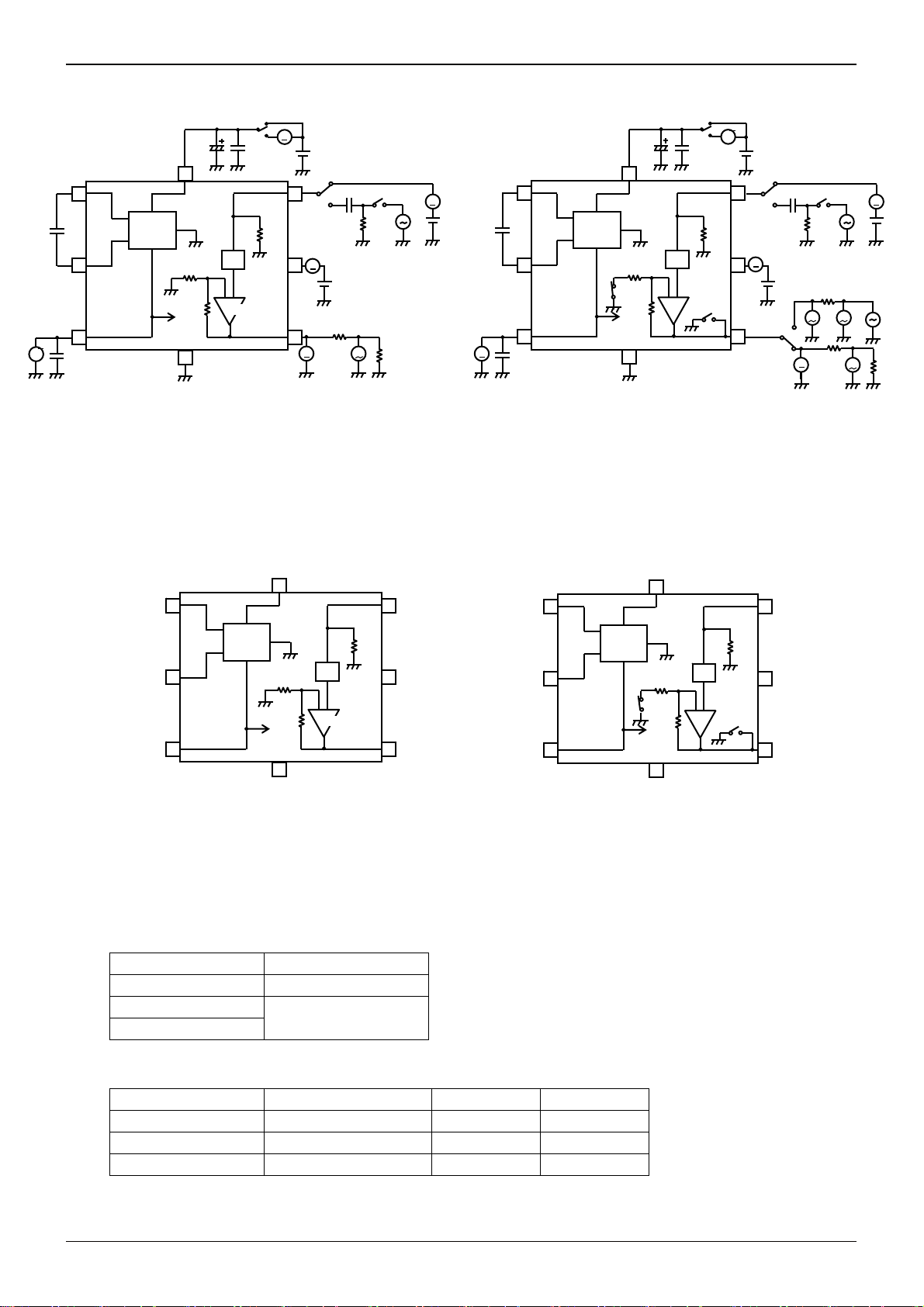
●Test Circuit Diagram
1.0uF
V
C_PLUS
C_MINUS
NVCC
1.0uF
10u
VCC
A2
A1
B1
C1
IN
CHARGE
PUMP
OUT
NVCC
LPF
6/9/12/16.5dB
GND
C2
0.01u
150k
A
(VCC)
1.0uF
V
C_PLUS
C_MINUS
NVCC
A1
B1
C1
1.0uF
VIN
A3
STBY
B3
VOUT
C3
0.1u
50Ω
A
75Ω
V
V
A
75Ω
(a) BH76906/09/12/16GU (b) BH76706GU
Fig. 1
CHARGE
PUMP
OUT
NVCC
Technical Note
A
0.01u
10u
VCC
A2
IN
150k
LPF
SW2
6dB
SW1
C2
GND
VIN
A3
STBY
B3
VOUT
C3
A
(VCC)
0.1u
50Ω
A
100Ω
V
75Ω
V
V
75Ω
※ A test circuit is a circuit for shipment inspection and differs from an application circuit example.
●Block Diagram
C_PLUS
A1
B1
C_MINUS
NVCC
C1
●Operation Logic
BH769xxGU
STBY Pin Logic Operating Mode
OPEN
BH76706GU
STBY Pin Logic Operating Mode SW1 SW2
※Use of the BH76706GU with the STBY pin OPEN is inappropriate
VCC
A2
IN
CHARGE
PUMP
OUT
NVCC
LPF
6/9/12/16.5dB
GND
C2
(a) BH76906/09/12/16GU
150k
VIN
A3
STBY
B3
VOUT
C3
C_PLUS
A1
B1
C_MINUS
NVCC
C1
VCC
A2
IN
CHARGE
PUMP
OUT
SW2
NVCC
6dB
C2
GND
(b) BH76706GU
LPF
Fig. 2
H Active
L
Standby
H Standby OFF OFF
M Input (Record) ON OFF
L Active (Playback) OFF ON
SW1
150k
VIN
A3
STBY
B3
VOUT
C3
www.rohm.com
3/16
© 2009 ROHM Co., Ltd. All rights reserved.
2009.03 - Rev.A
BH76906GU, BH76909GU, BH76912GU, BH76916GU, BH76706GU
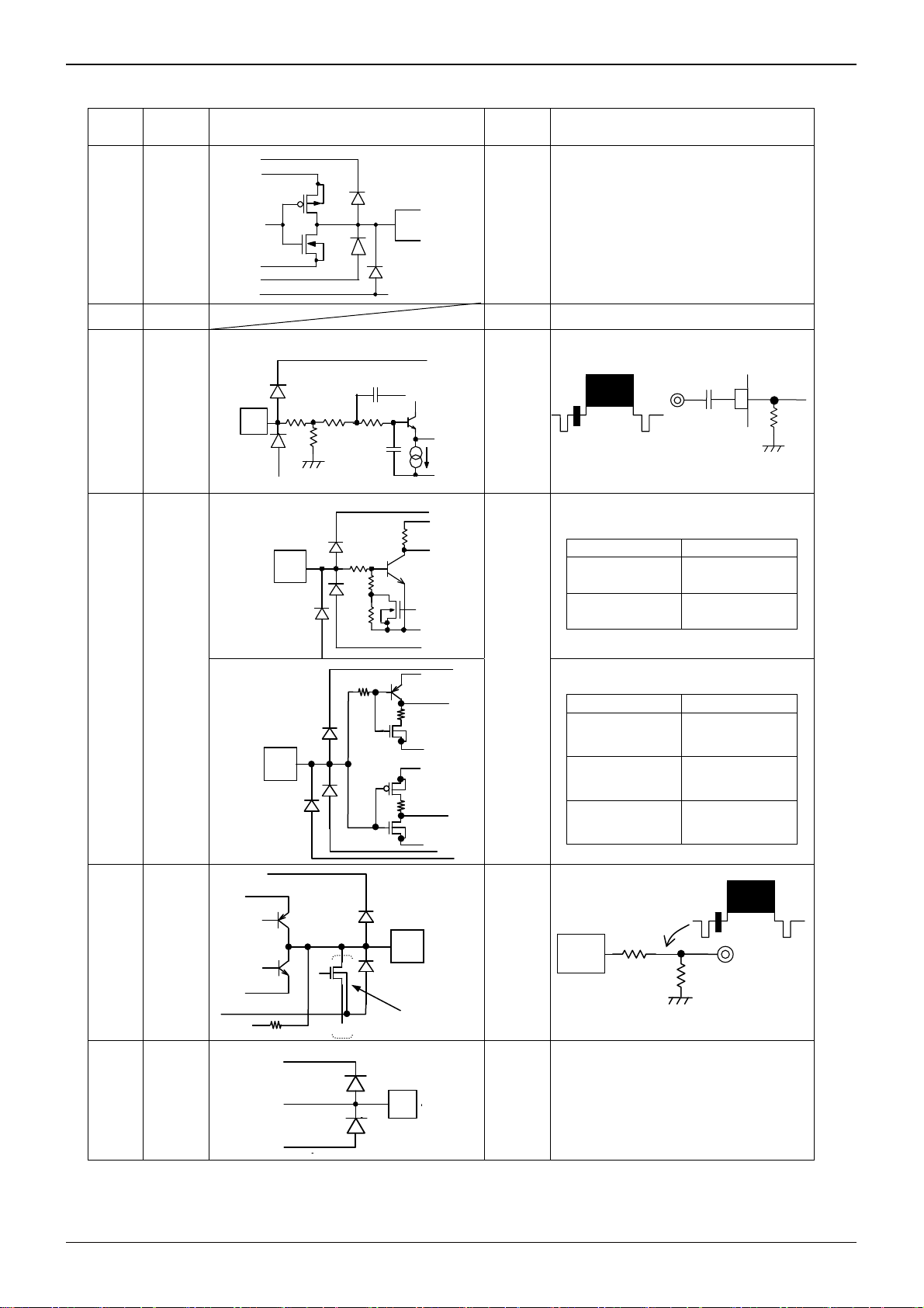
●Pin Descriptions
Ball
A1
Pin
Name
C_PLUS
Pin Internal Equivalent Circuit Diagram
VCC
VCC
C_PLUS
C1
DC
Voltage
+VCC
↑↓
Functional Description
Flying capacitor “+” pin
See functional descriptions of 7pin,
0V
GND
GND
NVCC
100
3.9k
4.1k
150K
VCC
3.9k
4.1k
VCC VCC pin
0V
Video signal input pin
Suitable input signals include
NV
composite video signals,
A2 VCC
A3 VIN
VIN
chroma signals, R.G.B. signals
50K
250K
200K
100K
VCC
VCC
vcc
200K
GND
GND
vcc
VCC
to
0V
ACTIVE/STANBY switching pin
Pin Voltage
1.2 V~VCC
( H )
0 V~0.45 V
( L )
MODE switching pin
Pin Voltage
B3 STBY
BH769xxGU
STBY
BH76706GU
2.8 V~VCC
STBY
GND
vcc
( H )
1.3 V~1.7 V
(M)
200K
GND
GND
NVCC
VCC
VCC
0 V~0.2 V
(L)
Video signal output pin
8pin
VIN
1μF
ACTIVE
STANBY
STANBY
GND (Record)
ACTIVE
(Playback)
Technical Note
150k
MODE
MODE
C3
VOUT
C2 GND
NVCC
NVCC
1K
VCC
NVCC
GND
VOUT
BH76706GU only
GND
0V
0V
VOUT
GND pin
75Ω
75Ω
Note 1) DC voltages in the figure are those when VCC = 3.0 V. Moreover, these values are reference values which are
not guaranteed.
Note 2) Numeric values in the figure are settings which do not guarantee ratings.
www.rohm.com
4/16
© 2009 ROHM Co., Ltd. All rights reserved.
2009.03 - Rev.A

BH76906GU, BH76909GU, BH76912GU, BH76916GU, BH76706GU
Technical Note
Flying capacitor “-“ pin (8pin)
C1
C2
NVC
0V
NVC
C1 NVCC
B1
C_MINUS
VCC
GND
GND
VCC
VCC
VCC
C_MINUS
C2
-VCC
(-2.75 V)
0V
↑↓
NVCC
-VCC
(-2.75 V)
Negative voltage pin (7pin)
Note 1) DC voltages in the figure are those when VCC = 3.0 V. Moreover, these values are reference values which are
not guaranteed.
Note 2) Numeric values in the figure are settings which do not guarantee ratings.
●Description of Operation
1) Principles of output coupling capacitorless video drivers
Single-supply amplifier
VCC
1000μF
1/2 VCC bias
Output capacitor required since DC
voltage is occurring at output pin
75Ω
75Ω
Dual-supply amplifier
VCC
-VCC
Output capacitor not required since
DC voltage does not occur at output
pin
75Ω
75Ω
Fig.3 Fig.4
For an amplifier operated from a single power supply (single-supply), since the operating point has a potential of
approximately 1/2 Vcc, a coupling capacitor is required for preventing direct current in the output. Moreover, since the
load resistance is 150 (75 + 75 ) for the video driver, the capacity of the coupling capacitor must be on the order of
1000 F if you take into account the low band passband. (Fig.3)
For an amplifier operated from dual power supplies (+ supply), since the operating point can be at GND level, a coupling
capacitor for preventing output of direct current is not needed.
Moreover, since a coupling capacitor is not needed, in principle, there is no lowering of the low band characteristic at the
output stage. (Fig.4)
2) Occurrence of negative voltage due to charge pump circuit
A charge pump, as shown in Fig. 5, consists of a pair of switches (SW1, SW2) and a pair of capacitors (flying capacitor,
anchor capacitor). Switching the pair of switches as shown in Fig. 5 causes a negative voltage to occur by shifting the
charge in the flying capacitor to the anchor capacitor as in a bucket relay.
In this IC, by applying a voltage of +3 V, a negative voltage of approximately -2.8 V is obtained.
www.rohm.com
5/16
© 2009 ROHM Co., Ltd. All rights reserved.
2009.03 - Rev.A

BH76906GU, BH76909GU, BH76912GU, BH76916GU, BH76706GU
V
V
Technical Note
cc +3V
SW1 SW2
Charge current
+
-
Flying capacitor
Anchor
Capacitor
Vcc +3V
Charge current
SW1
+
Charge current
Flying capacitor
SW2
-
Vcc occurs
-
-
Anchor Capacitor
+
cc +3V
Charging mode
-
+
Charge shi fting mode
-
+
+
-Vcc
-
occurs
Fig.5 Principles of Charge Pump Circuit
3) Configuration of BH769xxGU and BH76706GU
As shown in Fig. 6, a BH769xxGU or BH76706GU is a dual-supply amplifier and charge pump circuit integrated in one IC.
Accordingly, while there is +3 V single-supply operation, since a dual-supply operation amplifier is used, an output
coupling capacitor is not needed.
1μF
AMP
VCC
Dual-supply amplifier
75Ω
150k
VCC
75Ω
1-chip integration
Although single-supply,
output capacitor is not needed.
Charge pump
-VCC
1μF
Charge pump
1μF
Fig.6 Configuration Diagram of BH769xxGU or BH76706GU
4) Input pin format and sag characteristic
While a BH769xxGU or BH76706GU is a low voltage operation video driver, since it has a large dynamic range of
approximately 5.2 Vpp, a resistance termination method that is compatible regardless of signal form (termination by 150
k) is used, and not a clamp method that is an input method exclusively for video signals.
Therefore, since a BH769xxGU or BH76706GU operates normally even if there is no synchronization signal in the input
signal, it is compatible with not only normal video signals but also chroma signals and R.G.B. signals and has a wide
application range.
Moreover, concerning sag (lowering of low band frequency) that occurs at the input pin and becomes a problem for the
resistance termination method, since the input termination resistor is a high 150 k, even if it is combined with a small
capacity input capacitor, a sag characteristic that is not a problem in actual use is obtained.
In evaluating the sag characteristic, it is recommended that you use an H-bar signal in which sag readily stands out. (Fig.
8 to Fig. 10)
www.rohm.com
6/16
© 2009 ROHM Co., Ltd. All rights reserved.
2009.03 - Rev.A

BH76906GU, BH76909GU, BH76912GU, BH76916GU, BH76706GU
Technical Note
Input capacitor and input impedance cutoff frequency
is the same as when output capacitor in generic 75
driver is made 1000 F.
(Input pin time constant) (Output pin time constant)
1 F x 150 k = 1000 F x 150
a) Video signal without sag (TG-7/1 output, H-bar)
b) BH769xxGU or BH76706GU output (Input = 1.0 F, TG-7/1 output, H-bar)
c) 1000 F + 150 sag waveform (TG-7/1 output, H-bar)
Sag is determined
by input capacitor
and input resistor
only.
1μF
150k
Fig. 7
Fig. 8
TG-7/1
Fig. 9
Fig. 10
75Ω+75Ω=150Ω
Sag occurs
TV screen output image of
H-bar signal
Monitor
1μF
150k
BH769xxGU・BH76706GU
Nearly identical sag
75Ω
TG-7/1
75Ω
Monitor
1000μF
75Ω
75Ω
www.rohm.com
7/16
© 2009 ROHM Co., Ltd. All rights reserved.
2009.03 - Rev.A

BH76906GU, BH76909GU, BH76912GU, BH76916GU, BH76706GU
A
Technical Note
●Application Circuit Example
C_PLUS
C1=1.0uF C1=1.0uF
C_MINUS
NVCC
C2=1.0uF
t playback (Active mode) Recording (Input mode) BH76706GU only
NVCC
2.5~3.45V
Vcc
A2
SW2
C2
GND
LPF
6dB
C4=3.3uF
150k
SW1
A1
B1
C1
CHARGE
PUMP
NVCC
2.5~3.45V
Vcc
A2
SW2
C2
GND
C4=3.3uF
LPF
6/9/12/16.5dB
150k
SW1
C2=1.0uF
C_PLUS
A1
CHARGE
PUMP
B1
C_MINUS
NVCC
C1
C3=1.0uF C3=1.0uF
VIN
A3
VIDEO IN
STBY
B3
Video
monitor
CIRCUIT
CURREN
C3
VOUT
VIDEO OUT
R2=75Ω
VOUT
VIN
A3
STBY
B3
C3
VIDEO IN
R2=75Ω
VIDEO IN
75Ω
*SW1 and SW2 are built-in BH76706GU only See page 3/16 for STBY pin logic in each mode
Fig.11
※ We are confident in recommending the above application circuit example, but we ask that
you carefully check not just the static characteristics but also transient characteristics of this
circuit before using it.
●Caution on use
1. Wiring from the decoupling capacitor C4 to the IC should be kept as short as possible.
Moreover, this capacitor's capacitance value may have ripple effects on the IC, and may affect the S-N ratio for signals, so
we recommend using as large a decoupling capacitor as possible. (Recommended C4: 3.3 µF, B characteristics, 6.3 V
or higher maximum voltage)
Make mount board patterns follow the layout example shown on page 10 as closely as possible.
2. Capacitors to use
In view of the temperature characteristics, etc., we recommend a ceramic capacitor with B characteristics.
3. The NVCC (C1 pin) terminal generates a voltage that is used within the IC, so it should never be connected to a load
unless absolutely necessary. Moreover, this capacitor (C2) has a large capacitance value but very little negative voltage
ripple.
(Recommended C2: 1.0 F, B characteristic, 6.3 V or higher maximum voltage)
4. Capacitors C1 and C4 should be placed as close as possible to the IC. If the wiring to the capacitor is too long, it can
lead to intrusion of switching noise. (Recommended C1: 1.0 µF, B characteristics, 6.3 V or higher maximum voltage)
5. The HPF consists of input coupling capacitor C3 and 150 k of internal input impedance.
Be sure to check for video signal sag before determining the C3 value.
The cut-off frequency fc can be calculated using the following formula.
fc = 1/(2π×C3×150kΩ) (Recommended C3: 1.0 F, B characteristic, 6.3 V or higher maximum voltage)
6. The output resistor R2 should be placed close to the IC.
7. If the IC is mounted in the wrong direction, there is a risk of damage due to problems such as inverting VCC and GND.
Be careful when mounting it.
8. A large current transition occurs in the power supply pin when the charge pump circuit is switched. If this affects other
ICs (via the power supply line), insert a resistor (approximately 10 ) in the VCC line to improve the power supply's ripple
effects. Although inserting a 10
resistor lowers the voltage by about 0.2 V, this IC has a wide margin for low-voltage
operation, so dynamic range problems or other problems should not occur. (See Figures 12 to 14.)
www.rohm.com
8/16
© 2009 ROHM Co., Ltd. All rights reserved.
2009.03 - Rev.A

BH76906GU, BH76909GU, BH76912GU, BH76916GU, BH76706GU
Technical Note
1. Current ripple due to charge pump
circuit affects power supply Vcc pin
Vcc
Ω
10
1uF 3.3uF
2. Current ripple affects
DAC or other
Vcc pin
DAC
or
Other
1uF
V
IN
VIDEO
AMP
Ω
150k
V
OUT
-Vcc
75
Ω
75
Ω
Chrarge Pump
1uF
Fig.12 Effects of Charge Pump Circuit Current Ripple on External Circuit
1) Decoupling capacitor only
1) Decoupling capacitor only
Waveform of current between
power supply and capacitor (A)
10 mA/div
Waveform of current between
capacitor and IC (B)
10 mA/div
A
B
A
Fig.13
Vcc
2) Decoupling capacitor + 10 resistor
2) Decoupling capacitor + 10 resistor
Waveform of current between
power supply and capacitor (A)
10 mA/div
Waveform of current between
resistor and capacitor (B)
10 mA/div
Waveform of current between
capacitor and IC (C)
10 mA/div
10
Ω
A
A
B
A
C
Vcc
Fig.14
www.rohm.com
9/16
© 2009 ROHM Co., Ltd. All rights reserved.
2009.03 - Rev.A
Vcc
A
Vcc
A

BH76906GU, BH76909GU, BH76912GU, BH76916GU, BH76706GU
●Evaluation Board Pattern Diagram (Double-sided, 2 layers)
Parts List
Symbol Function Recommended Value Remarks
C1 Flying capacitor 1μF B characteristic recommended
C2 Tank capacitor 1μF B characteristic recommended
C3 Input coupling capacitor
C4 Decoupling capacitor 3.3μF B characteristic recommended
R1 Input termination resistor 75Ω Needed when connected to video signal measurement set
R2 Output resistor 75Ω ―
R3 Output termination resistor 75Ω
Input connector BNC
Output connector RCA (Pin jack)
Fig.15
1μF
B characteristic recommended
Not needed when connected to TV or video signal
measurement set
Layer 1 wiring + Silkscreen legend
Layer 2 wiring
Solder pattern
Technical Note
www.rohm.com
10/16
© 2009 ROHM Co., Ltd. All rights reserved.
2009.03 - Rev.A

BH76906GU, BH76909GU, BH76912GU, BH76916GU, BH76706GU
g
Technical Note
●Reference Data
BH76906GU
30
25
20
15
10
CIRCUIT CURRENT [mA]
5
0
01234
STANDBY CURRENT [uA]
POWER SUPPLY VOLTAGE [V]
Fig. 16 Circuit Current vs Supply
Volta
BH76906GU
0.4
0.3
0.2
0.1
0
Ta= 2 5℃
e
VCC=3V
-0.1
-80 -40 0 40 80 120
Fig. 19 Standby Circuit Current
TEMPERATURE [℃]
vs Ambient Temperature
5
BH76906GU
Ta= 2 5℃
0
-5
-10
VOUT DC OFFSET [mV]
-15
2 2.5 3 3.5 4
POWER SUPPLY VOLTAGE [V]
Fig. 22 VOUT Pin Output DC Offset
vs Supply Voltage
BH76906GU
25
20
15
10
CIRCUIT CURRENT [mA]
5
-80 -40 0 40 80 120
TEMPERATURE [℃]
Fig. 17 Circuit Current
vs Ambient Temperature
BH76706GU
200
150
100
50
CIRCUIT CURRENT [μA] CIRCUIT CURRENT [μA]
0
22.533.54
POWER SUPPLY VOLTAGE
[V]
Ta= 2 5℃
Fig. 20 GND Mode Circuit Current
vs Supply Voltage
BH76906GU
5
0
-5
-10
VOUT DC OFFSET [mV]
-15
-80 -40 0 40 80 120
TEMPERATURE [℃]
Fig. 23 VOUT Pin Output DC Offset
vs Ambient Temperature
VCC=3V
VCC=3V
BH76906GU
0.4
0.3
0.2
0.1
0
STANDBY CURRENT [uA]
-0.1
22.533.54
POWER SUPPLY VOLTAGE [V]
Fig. 18 Standby Circuit Current
vs Supply Voltage
BH76706GU
200
150
100
50
CIRCUIT CURRENT [μA]
0
-80 -40 0 40 80 120
BH76906GU
10
0
-10
-20
-30
-40
-50
VOLTAGE GAIN [dB]
-60
-70
-80
1.E+06 1.E+07 1.E+08
TEMPERATURE [℃]
VCC=3V Ta=25℃
FREQUENCY [Hz]
Fig. 24 Frequency Characteristic
Ta= 2 5℃
VCC=3V
BH76706GU
10
0
-10
-20
-30
-40
-50
VOLTAGE GAIN [dB]
-60
-70
-80
1.E+06 1.E+07 1.E+08
FREQUENCY [Hz]
VCC=3V Ta=25℃
Fig. 25 Frequency Characteristic
www.rohm.com
11/16
© 2009 ROHM Co., Ltd. All rights reserved.
BH76906GU
6.2
6.1
6
5.9
VOLTAGE GAIN [dB]
5.8
22.533.54
POWER SUPPLY VOLTAGE [V]
Fig. 26 Voltage Gain vs Supply Voltage
Ta= 2 5℃
VOLTAGE GAIN [dB]
Fig. 27 Voltage Gainvs Ambient Temperature
BH76906GU
6.2
6.1
6
5.9
5.8
-80 -40 0 40 80 120
TEMPERATURE [℃]
VCC=3V
2009.03 - Rev.A

BH76906GU, BH76909GU, BH76912GU, BH76916GU, BH76706GU
VCC=3V
0.4
BH76906GU
Ta= 2 5℃
BH76906GU
0.4
0.2
0
f=4.5MHz/100kHz
0.2
0
f=4.5MHz/100kHz
BH76906GU
-1
-2
-3
Technical Note
Ta= 2 5℃
f=8MHz/100kHz
-0.2
FREQUENCY RESPONSE1:Gf1[dB]
-0.4
22.533.54
POWER SUPPLY VOLTAGE
[V]
Fig. 28 Frequency Characteristic 1
vs Supply Voltage
BH76906GU
-1
-2
-3
-4
FREQUENCY RESPONSE2:Gf2[dB]
-5
-80 -40 0 40 80 120
TEMPERATURE [℃]
VCC=3V
f=8MHz/100kHz
Fig. 31 Frequency Characteristic 2
vs Ambient Temperature
-0.2
FREQUENCY RESPONSE1:Gf1[dB]
-0.4
-80 -40 0 40 80 120
TEMPARATURE [℃]
Fig. 29 Frequency Characteristic 1
vs Ambient Temperature
BH76906GU
-20
-25
-30
-35
FREQUENCY RESPONSE3:Gf3[dB]
22.533.54
POWER SUPPLY VOLTAGE [V]
f=18MHz/100kHz
f=18MHz/100kHz
Ta= 2 5℃
Fig.32 Frequency Characteristic 3
vs Supply Voltage
-4
FREQUENCY RESPONSE2:Gf2[dB]
-5
22.533.54
POWER SUPPLY VOLTAGE [V]
Fig. 30 Frequency Characteristic 2
vs Supply Voltage
BH76906GU
-20
f=18MHz/100kHz
-25
-30
-35
FREQUENCY RESPONSE3:Gf3[dB]
-80 -40 0 40 80 120
TEMPERATURE [℃]
VCC=3V
BH76906GU
-35
-40
-45
f=23.5MHz/100k
FREQUENCY RESPONSE4:Gf4[dB]
-50
22.533.54
POWER SUPPLY VOLTAGE [V]
Hz
Fig. 34 Frequency Characteristic4
vs Supply Voltage
BH76906GU
6
5.8
5.6
5.4
5.2
MAX OUTPUT VOLTAGE [Vpp]
Ta= 2 5℃
VCC=3V
BH76906GU
-35
-40
-45
f=23.5MHz/100k
FREQUENCY RESPONSE4:Gf4[dB]
-50
-80 -40 0 40 80 1 20
TEMPERATURE [℃]
Hz
Fig. 35 Frequency Characteristic 4
vs Ambient Temperature
3
2
1
6dB
0
9dB
12dB
16.5dB
-1
OUTPUT DC VOLTAGE [V]
-2
VCC=3V Ta =2 5 ℃
VCC=3V
BH76906GU
7
6
5
4
MAX OUTPUT VOLTAGE [Vpp]
3
22.533.54
POWER SUPPLY VOLTAGE [V]
Ta= 2 5℃
5
-80 -40 0 40 80 120
TEMPARATURE [℃]
Fig. 37 Max. Output Level vs Ambient Temperature
www.rohm.com
12/16
© 2009 ROHM Co., Ltd. All rights reserved.
-3
-1.5 -1.0 -0.5 0.0 0.5 1.0 1.5
INPUT DC VOLTAGE [V]
Fig. 38 DC I/O Characteristic
2009.03 - Rev.A

BH76906GU, BH76909GU, BH76912GU, BH76916GU, BH76706GU
Technical Note
CHARGEPUMP OSC FREQUENCY [KHz]
BH76906GU
230
225
220
215
210
205
200
22.533.54
POWER SUPPLY VOLTAGE [V]
Ta= 2 5℃
Fig. 39 Charge Pump Oscillation Frequency
vs Supply Voltage
BH76906GU
-1
-1.5
-2
-2.5
-3
-3.5
CHARGEPUMP OUTPUT VOLTAGE [V]
-4
22.533.54
POWER SUPPLY VOLTAGE [V]
Ta= 2 5℃
Fig. 41 Charge Pump Output Voltage
vs Supply Voltage
BH76906GU
230
225
220
215
210
CHARGEPUMP OSC FREQUENCY [KHz]
205
-80 -40 0 40 80 120
TEMPERATURE [℃]
VCC=3V
Fig. 40 Charge Pump Oscillation Frequency
vs Ambient Temperature
BH76906GU
-1.0
-1.5
-2.0
-2.5
CHARGEPUMP OUTPUT VOLTAGE [V]
-3.0
0.0 10.0 20.0 30.0 40.0
LOAD CURRENT [mA]
VCC=3V Ta=25℃
Fig. 42 Charge Pump Load Regulation
BH76912GU
1.2
1.1
1
0.9
DIFFERENTIAL PHASE [Deg]
0.8
22.533.54
POWER SUPPLY VOLTAGE [V]
Ta= 2 5℃
DIFFERENTIAL PHASE [Deg]
BH76912GU
1.2
1.1
1
0.9
0.8
-80 -40 0 40 80 120
TEMPERATURE [℃]
VCC=3V
Fig. 43 Differential Phase
vs Supply Voltage
BH76912GU BH76912GU
0.8
0.6
0.4
0.2
DIFFERENTIAL GAIN [%]
Ta= 2 5℃
0.8
0.6
0.4
0.2
DIFFERENTIAL GAIN [%]
VCC=3V
0
22.533.54
POWER SUPPLY VOLTAGE [V]
Fig. 45 Differential Gain
vs Supply Voltage
www.rohm.com
13/16
© 2009 ROHM Co., Ltd. All rights reserved.
0
-80 -40 0 40 80 120
TEMPERATURE [℃]
Fig. 46 Differential Gain
vs Ambient Temperature
2009.03 - Rev.A

BH76906GU, BH76909GU, BH76912GU, BH76916GU, BH76706GU
BH76906GU BH76906GU
79
Ta= 2 5℃
79
Technical Note
VCC=3V
78.5
78
Y S/N [dB]
77.5
77
2 2 .5 3 3 .5 4
POWER SUPPLY VOLTAGE [V]
Fig. 47 Y S/N vs Supply Voltage
BH76906GU
80
78
76
74
CHROMA S/N (AM) [dB]
72
70
2 2.5 3 3.5 4
POWER SUPPLY VOLTAGE [V]
Ta= 2 5℃
Fig. 49 C AM S/N vs Supply Voltage
78.5
78
Y S/N [dB]
77.5
77
-80 -40 0 40 80 120
TEMPERATURE [℃]
Fig.48 Y S/N vs Ambient Temperature
BH76906GU
80
78
76
74
CHROMA S/N (AM) [dB]
72
70
-80 -40 0 40 80 120
TEMPERATURE [℃]
VCC=3V
Fig. 50 C AM S/N vs Ambient Temperature
BH76906GU
70
68
66
64
CHROMA S/N (PM) [dB]
62
60
22.5 33.54
POWER SUPPLY VOLTAGE [V]
Ta= 2 5℃
Fig. 51 C PM S/N vs Supply Voltage
BH76906GU
180
165
150
135
INPUT IMPEDANCE [kΩ]
Ta= 2 5℃
BH76906GU
70
68
66
64
CHROMA S/N (PM) [dB]
62
60
-80 -40 0 40 80 120
TEMPERATURE [℃]
VCC=3V
Fig. 52 C PM S/N vs Ambient Temperature
BH76906GU
165
150
135
INPUT IMPEDANCE [kΩ]
VCC=3V
120
22.533.54
POWER SUPPLY VOLTAGE [V]
Fig. 53 Input Impedance vs Supply Voltage
www.rohm.com
14/16
© 2009 ROHM Co., Ltd. All rights reserved.
120
-80 -40 0 40 80 120
TEMPERATURE [℃]
Fig. 54 Input Impedance vs Ambient Temperature
2009.03 - Rev.A

BH76906GU, BH76909GU, BH76912GU, BH76916GU, BH76706GU
BH76906GU
20
VCC=3V Ta=25℃
BH76706GU
20
Technical Note
VCC=3V Ta=25℃
16
12
8
4
CIRCUIT CURRENT [mA]
0
0.0 0.5 1.0 1.5 2.0 2.5 3.0
CTL TERMINAL VOLTAGE [V]
Fig. 55 Control Pin Characteristic
16
12
8
CIRCUIT CURRENT [mA]
4
0
0 0.5 1 1.5 2 2.5 3
CTL TERMINAL VOLTAGE [V]
Fig. 56 Control Pin Characteristic
5
BH76706GU
Ta= 2 5℃
BH76706GU
5
VCC=3V
4
4
3
3
2
ON RESISTANCE [Ω]
2
ON RESISTANCE [Ω]
1
22.5 33.5 4
POWER SUPPLY VOLTAGE [V]
1
-80 -40 0 40 80 120
POWER SUPPLY VOLTAGE [V]
Fig. 57 Output Pin Shunt Switch On Resistance
vs Supply Voltage
Fig. 58 Output Pin Shunt Switch On Resistance
vs Ambient Temperature
● Performing separate electrostatic damage countermeasures
When adding an externally attached electrostatic countermeasure element to the output pin, connect a varistor in the
position shown in Fig. 59 (if connected directly to the output pin, the IC could oscillate depending on the capacity of the
varistor). For this IC, since the output waveform is GND-referenced and swings positive and negative, a normal Zener
diode cannot be used.
ESD or surge
VOUT
75Ω
75Ω
Fig.59 Using Externally Attached Varistor
www.rohm.com
15/16
© 2009 ROHM Co., Ltd. All rights reserved.
2009.03 - Rev.A

BH76906GU, BH76909GU, BH76912GU, BH76916GU, BH76706GU
●Selection of order type
VCSP85H1
<Dimension>
B H 7 6 9 0 E 2
Part. No.
BH76906GU
BH76909GU
BH76912GU
BH76916GU
BH76706GU
Tape Embossed carrier tape
Quantity 3000pcs
Direction
of feed
(Unit:mm)
6
E2
(The direction is the 1pin of product is at the upper left when you hold
reel on the left hand and you pull out the tape on the right hand)
1234 1234 1234 1234 1234 1234
Reel
G U
1pin
※When you order , please order in times the amount of package quantity.
Technical Note
Tape and Reel information
Direction of feed
www.rohm.com
16/16
© 2009 ROHM Co., Ltd. All rights reserved.
2009.03 - Rev.A

Notes
No copying or reproduction of this document, in part or in whole, is permitted without the
consent of ROHM Co.,Ltd.
The content specied herein is subject to change for improvement without notice.
The content specied herein is for the purpose of introducing ROHM's products (hereinafter
"Products"). If you wish to use any such Product, please be sure to refer to the specications,
which can be obtained from ROHM upon request.
Examples of application circuits, circuit constants and any other information contained herein
illustrate the standard usage and operations of the Products. The peripheral conditions must
be taken into account when designing circuits for mass production.
Great care was taken in ensuring the accuracy of the information specied in this document.
However, should you incur any damage arising from any inaccuracy or misprint of such
information, ROHM shall bear no responsibility for such damage.
The technical information specied herein is intended only to show the typical functions of and
examples of application circuits for the Products. ROHM does not grant you, explicitly or
implicitly, any license to use or exercise intellectual property or other rights held by ROHM and
other par ties. ROHM shall bear no responsibility whatsoever for any dispute arising from the
use of such technical information.
Notice
The Products specied in this document are intended to be used with general-use electronic
equipment or devices (such as audio visual equipment, ofce-automation equipment, communication devices, electronic appliances and amusement devices).
The Products specied in this document are not designed to be radiation tolerant.
While ROHM always makes efforts to enhance the quality and reliability of its Products, a
Product may fail or malfunction for a variety of reasons.
Please be sure to implement in your equipment using the Products safety measures to guard
against the possibility of physical injury, re or any other damage caused in the event of the
failure of any Product, such as derating, redundancy, re control and fail-safe designs. ROHM
shall bear no responsibility whatsoever for your use of any Product outside of the prescribed
scope or not in accordance with the instruction manual.
The Products are not designed or manufactured to be used with any equipment, device or
system which requires an extremely high level of reliability the failure or malfunction of which
may result in a direct threat to human life or create a risk of human injury (such as a medical
instrument, transportation equipment, aerospace machiner y, nuclear-reactor controller,
fuel-controller or other safety device). ROHM shall bear no responsibility in any way for use of
any of the Products for the above special purposes. If a Product is intended to be used for any
such special purpose, please contact a ROHM sales representative before purchasing.
If you intend to export or ship overseas any Product or technology specied herein that may
be controlled under the Foreign Exchange and the Foreign Trade Law, you will be required to
obtain a license or permit under the Law.
Thank you for your accessing to ROHM product informations.
More detail product informations and catalogs are available, please contact us.
ROHM Customer Support System
www.rohm.com
© 2009 ROHM Co., Ltd. All rights reserved.
http://www.rohm.com/contact/
R0039
A
 Loading...