

A
High-performance Video Signal Switchers
Video・Audio Signal Switchers
for Car Navigation Car DVD Player
BH7649KS2
●Description
BH7649KS2 is built-in video switch, audio switch and isolation amplifier in a single chip.
●Features
1) Video inputs selector: 7-inputs composite, Video outputs: 2-outputs 75Ω video driver, 2-outputs AMP
2) Built in Video gain switch (-6dB / -3dB / 0dB / 3dB)
3) Built in Video LPF switch (6.75MHz / Through)
4) Built in sag compensation circuit
5) Enables two load drivers
6) Video driver: Able to be used without load
7) Video driver : Able to be used without output coupling capacitor(one load)
8) Audio inputs selector: 5-inputs(Lch, Rch), Audio outputs : 2-outputs(Lch, Rch)
9) Built in Audio gain switch (0dB / -6dB)
10) Built in Audio LPF switch (24kHz / Through)
11) Built in MUTE function
12) Audio/Video all inputs: Built in isolator function
13) Selectable isolator function for different Audio/Video input channels
14) Serial control with I
15) Optional Slave address modifications (90H / 92H)
●Applications
Car navigation, Car DVD
●Absolute maximum ratings (Ta=+25℃)
2
C-BUS (I2C-BUS is compatible with fast mode of Version2.0)
No.11066EAT05
Parameter Symbol Ratings Unit
Supply voltage VVcc VVccmax 10 V
Supply voltage AVcc AVccmax 10 V
Power dissipation Pd 1900 *1 mW
Input voltage range I2C-BUS input
(SCL, SDA)
Input voltage range Video selector, LOGIC
(VIN1, VRET1, VIN2, VRET2, VIN3, VRET3, VIN4, VRET4,
VIN5, VRET5, VIN6, VRET6, VIN7, VRET7, ADR)
Input voltage range Video driver
(VDIN1, VDIN2)
Input voltage range Audio seletor
(LIN1, ARET1, RIN1, LIN2, ARET2, RIN2, LIN3, ARET3, RIN3,
LIN4, ARET4, RIN4, LIN5, ARET5, RIN5)
V
-0.2 ~ 7.0 V
I2CIN
V
-0.2 ~ 5.1 V
IN1
-0.2 ~ VVcc+0.2 V
V
DIN1
V
-0.2 ~ AVcc+0.2 V
AIN1
Storage temperature range Tstg -55~+125 ℃
*1 When mounting on a 70mm×70mm×1.6mm 4-layer glass epoxy board
Reduced by 19mW/℃ at Ta = +25℃ or higher
●Operating conditions
Parameter
Symbol Ratings Unit
Supply voltage VVcc VVcc +7.5 ~ +9.5 V
Supply voltage AVcc AVcc +7.5 ~ +9.5 V
Operating temperature range Topr -40 ~ +85 ℃
* This product is not designed for protection against radioactive rays.
www.rohm.com
1/12
© 2011 ROHM Co., Ltd. All rights reserved.
2011.04 - Rev.
A
BH7649KS2
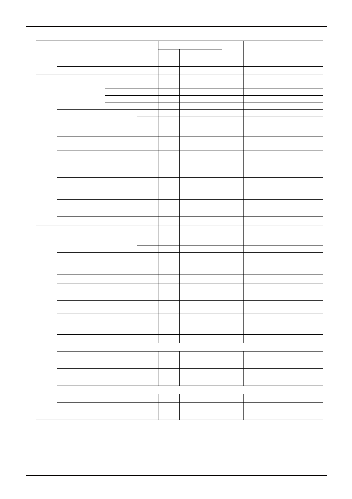
●Electric characteristic (Unless otherwise specified, Ta=+25℃, VVcc=8.5V, AVcc=8.5V)
Limits
Unit Conditions
CHIP
Parameter Symbol
Min. Typ. Max.
Circuit current1 ICC1 - 34 48 mA No signal(VIDEO)
Circuit current2 ICC2 - 23 32 mA No signal(AUDIO)
-6dB GVM6V-6.4 -6.0 -5.6 dB Vin=1.0Vpp, f=100kHz
-3dB GVM3V-3.4 -3.0 -2.6 dB Vin=1.0Vpp, f=100kHz
VIDEO
Voltage gain
Frequency characteristics1
[f=6.75MHz LPF MODE]
Frequency characteristics 2_1
[THROUGH MODE_-6dB]
Frequency characteristics 2_2
[THROUGH MODE_-3dB]
Frequency characteristics 2_3
[THROUGH MODE_0dB]
Frequency characteristics 2_4
[THROUGH MODE_3dB]
Frequency characteristics 3
[VDOUT1, VDOUT2]
Maximum output level VOM
0dB GV0
3dB GV3
6dB GV6
GF11
GF12
GF2
GF2
GF2
GF2
GF3
-0.4 0.0 0.4 dB Vin=1.0Vpp, f=100kHz
V
2.6 3.0 3.4 dB Vin=1.0Vpp, f=100kHz
V
5.6 6.0 6.4 dB Vin=1.0Vpp, f=100kHz
V
-1.5 0.0 1.0 dB Vin=1.0Vpp, f=6.75MHz/100kHz
V
- -30 -20 dB Vin=1.0Vpp, f=27MHz/100kHz
V
-0.6 0.9 1.9 dB
V
-0.7 0.8 1.8 dB
V
-0.7 0.8 1.8 dB
V
-1.0 0.5 1.5 dB
V
-3.0 -0.5 1.0 dB Vin=1.0Vpp, f=15MHz
V
2.6 - - Vp-p f=10kHz, THD=1.0%
V
Cross talk CTV - -60 -50 dB Vin=1.0Vpp, f=4.43MHz
MUTE attenuation MTV - -60 -50 dB Vin=1.0Vpp, f=4.43MHz
Common mode rejection ratio CMRR - -60 -40 dB Vin=1Vpp, f=20kHz
Voltage gain
0dB GV0
-6dB GV6
Frequency characteristics 1
[f=24kHz LPF MODE]
Frequency characteristics 2
[THROUGH MODE]
GF11
GF12
GF2
-0.4 0.0 0.4 dB Vin=1Vrms, f=1kHz
A
-6.4 -6.0 -5.6 dB Vin=1Vrms, f=1kHz
A
-2.0 -0.5 1.0 dB Vin=1Vrms, f=24kHz/1kHz
A
- -26 -15 dB Vin=1Vrms, f=96kHz/1kHz
A
-1.0 0.0 1.0 dB Vin=1Vrms, f=50kHz/1kHz
A
Total harmonic distortion THD+N - 0.002 0.1 % Vin=1Vrms, f=1kHz ※1
AUDIO
Maximum output level VOM
Cross talk CTA - -100 -85 dB Vin=2Vrms, f=1kHz ※1
2.0 2.4 - Vrms f=1kHz, THD<0.3% ※1
A
MUTE attenuation MTA - -100 -85 dB Vin=2Vrms, f=1kHz ※1
Residual noise1
[THROUGH MODE]
Residual noise2
[f=24kHz LPF MODE]
NA - 10 - uVrms
N
A_LPF
- 20 - uVrms
Common mode rejection ratio CMRR - -70 -40 dB Vin=1Vrms, f=1kHz
PSRR PSRR
- -50 - dB ※3
A
[SCL,SDA]
VIL ※4 Vin1L 0 - 1.0 V Low Level input voltage
VIH ※4 Vin1H 2.0 - 5.5 V High Level input voltage
Input bias current IINI2C -10 0 10 uA
I2C
SDA output voltage VoL 0 - 0.4 V at 3.0mA sink current
[ADR]
VIL Vin2L 0 - 1.0 V Low Level input voltage
VIH Vin2H 2.0 - 5.1 V High Level input voltage ※5
Input impedance ZIN
※1 400HzHPF + 30kHzLPF ON
※2 IHF-A Filter ON
※3 Vin=0.3Vpp, f=100Hz at VCC, 30kHzLPF ON
2
C-BUS(SCL,SDA) SPEC> VIL:-0.5[V]~0.3VDD[V], VIH:0.7 VDD[V]~VDD+0.5 or 5.5[V] (VDD:I2C-BUS_Supply voltage)
※4 <I
<BH7649KS2> Be sure to use as VIL:0.0[V]~1.0[V], VIH:2.0[V]~5.5[V]
※5 We recommend that it is connect ADR Pin to 38Pin(VREG Pin) when ADR Pin is used as “H”.
70 100 130 kΩ Pull-Down Resister
ADR
Technical Note
Vin=1.0Vpp, f=10MHz/100kHz
Gain=-6dB
Vin=1.0Vpp, f=10MHz/100kHz
Gain=-3dB
Vin=1.0Vpp, f=10MHz/100kHz
Gain=0dB
Vin=1.0Vpp, f=10MHz/100kHz
Gain=3dB
(THROUGH MODE select)
※2
LOUT1, ROUT1(LPF select)
※2
www.rohm.com
2/12
© 2011 ROHM Co., Ltd. All rights reserved.
2011.04 - Rev.
A
BH7649KS2
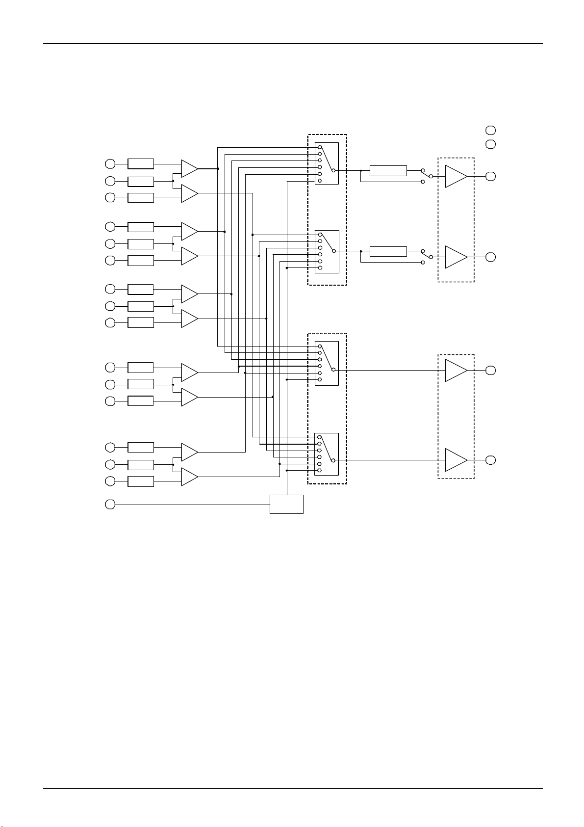
●Block Diagram (Audio block)
LIN1 2
ARET1 3
RIN1 4
Bias
Bias
Bias
LIN2 6
Bias
ARET2 7
RIN2 8
Bias
Bias
LIN3 10
ARET3 11
RIN3 12
Bias
Bias
Bias
LIN 4 14
ARET4 15
RIN4 16
Bias
Bias
Bias
LIN5 18
ARET5 19
RIN5 20
Bias
Bias
Bias
ABIAS 5
Audi o_SEL1
MUTE
MUTE
Audio_SEL2
MUTE
MUTE
BIAS
Fig.1 Block Diagram
LPF_Au dio
LPF_Au dio
Technical Note
Audio_Gain1
0/-6dB
0/-6dB
Audio_Gain2
0/-6dB
0/-6dB
13 AVcc
9 AGND
22 LOUT1
23 ROUT1
24 LOUT2
25 ROUT2
www.rohm.com
3/12
© 2011 ROHM Co., Ltd. All rights reserved.
2011.04 - Rev.
A
BH7649KS2
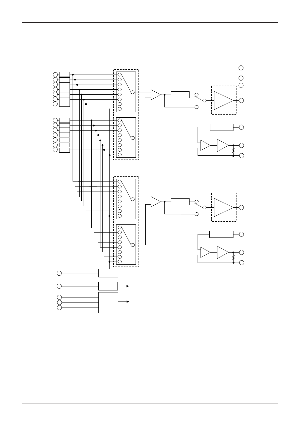
●Block Diagram (Video block)
VIN1
VIN2
VIN3
VIN4
VIN5
VIN6
VIN7
Bias
39
Bias
41
43
Bias
Bias
45
47
Bias
49
Bias
51
Bias
VRET1
VRET2
VRET3
VRET4
VRET5
VRET6
VRET7
42
Bias
Bias
44
Bias
46
Bias
48
Bias
50
52
Bias
Bias
40
VBIAS
21
VREG
38
ADR
SDA
SCL
17
36
37
BIAS2
VREG
LOGIC
Video_SEL1
MUTE
MUTE
Video_SEL2
MUTE
MUTE
Fig.2 Block Diagram
LPF_Video1
LPF_Video2
6dB
6dB
Video_Gain1
-6/-3/
0/3dB
Clamp/Bias1
75Ω
Video_Gain2
-6/-3/
0/3dB
Clamp/Bias2
75Ω
Technical Note
VVcc
26
31
VGND1
VGND2
1
VOUT1
35
34 VDIN1
VDOUT1
27
28 VDSAG1
VOUT2
33
VDIN2
32
VDOUT2
29
30
VDSAG2
www.rohm.com
4/12
© 2011 ROHM Co., Ltd. All rights reserved.
2011.04 - Rev.

A
BH7649KS2
●Package outlines
●Pin assignment table
Technical Note
BH7649KS2
Lot No.
SQFP-T52(UNIT:mm )
Fig.3 Package outlines
No. I/O Pin Name No. I/O Pin Name No. I/O Pin Name No. I/O Pin Name
1 - VGND2 14 I LIN4 27 O VDOUT1 40 I VRET1
2 I LIN1 15 I ARET4 28 O VDSAG1 41 I VIN2
3 I ARET1 16 I RIN4 29 O VDOUT2 42 I VRET2
4 I RIN1 17 I ADR 30 O VDSAG2 43 I VIN3
5 - ABIAS 18 I LIN5 31 - VGND1 44 I VRET3
6 I LIN2 19 I ARET5 32 I VDIN2 45 I VIN4
7 I ARET2 20 I RIN5 33 O VOUT2 46 I VRET4
8 I RIN2 21 - VBIAS 34 I VDIN1 47 I VIN5
9 - AGND 22 O LOUT1 35 O VOUT1 48 I VRET5
10 I LIN3 23 O ROUT1 36 I/O SDA 49 I VIN6
11 I ARET3 24 O LOUT2 37 I SCL 50 I VRET6
12 I RIN3 25 O ROUT2 38 O VREG 51 I VIN7
13 - AVcc 26 - VVcc 39 I VIN1 52 I VRET7
www.rohm.com
5/12
© 2011 ROHM Co., Ltd. All rights reserved.
2011.04 - Rev.

A
BH7649KS2
Technical Note
●I2C-BUS Control specification I
SLAVE
S
ADDRESS
A DATA1 A DATA2 A DATA3 A DATA4 A DATA5 A DATA6 A P
2
C-BUS Format (WRITE MODE)
S : Start Condition
A : Acknowledge
P : Stop Condition
b7 b6 b5 b4 b3 b2 b1 b0
SLAVE
ADDRESS
DATA1 Video_SEL1 Video_SEL2 LPF_Video1 LPF_Video2
DATA2 Video_Gain1 Video_Gain2 Clamp/Bias1 Clamp/Bias2
DATA3 Audio_SEL1 Audio_SEL2 0 LPF_Audio
DATA4 0 0 Audio_Gain1 Audio_Gain2 0 0 0 0
DATA5 Isolation_V1 Isolation_V2 Isolation_V3 Isolation_V4 Isolation_V5 Isolation_V6 Isolation_V7 0
DATA6 Isolation_A1 Isolation_A2 Isolation_A3 Isolation_A4 Isolation_A5 0 0 0
When power is turned on, all parts start from LOW condition.
[Prohibited matter] The terminal inputs of ADR do not change from start to stop condition. Operation error might happen.
1 0 0 1 0 0 ADR 0
Video_power
-off1
Video_power
-off2
www.rohm.com
6/12
© 2011 ROHM Co., Ltd. All rights reserved.
2011.04 - Rev.

A
BH7649KS2
●Selecting input switch / Setting mode
Data name Status Data name Status Data name Status
ADR
Video_SEL1
000 : VIN1
001 : VIN2
010 : VIN3 Video_power-off1
011 : VIN4 0 : On 0 : On
100 : VIN5 1 : Off 1 : Off
101 : VIN6 Video_power-off2
110 : VIN7 0 : On 0 : On
111 : MUTE 1 : Off 1 : Off
Video_SEL2
000 : VIN1 000 : LIN1, RIN1 0 : On
Sets the slave address by
ADR pin
0 : 90H
ADR pin = “ L ”
1 : 92H
ADR pin =” H ”
Signal input selectors
(Video_SEL1)
Signal input selectors
(Video_SEL2)
Clamp/Bias1
Clamp/Bias2
Audio_ SEL1
Input mode selectors
(Clamp/Bias1 : VDIN1)
0 : Clamp input mode
(VDOUT1:direct drive)
1 : Bias input mode
(VDOUT1:output coupling “C”)
Input mode selectors
(Clamp/Bias2 : VDIN2)
0 : Clamp input mode
(VDOUT2 direct drive)
1 : Bias input mode
(VDOUT2:output coupling “C”)
Power-off function selectors
(VDIN1 - VDOUT1)
Power-off function selectors
(VDIN2 - VDOUT2)
Signal input selectors
(Audio_ SEL1)
Isolation_V1 Isolator function selectors (VIN1)
0 : On
1 : Off
Isolation_V2 Isolator function selectors (VIN2)
0 : On
1 : Off
Isolation_V3 Isolator function selectors (VIN3)
Isolation_V4 Isolator function selectors (VIN4)
Isolation_V5 Isolator function selectors (VIN5)
Technical Note
001 : VIN2 001 : LIN2, RIN2 1 : Off
010 : VIN3 010 : LIN3, RIN3 Isolation_V6 Isolator function selectors (VIN6)
011 : VIN4 011 : LIN4, RIN4 0 : On
100 : VIN5 100 : LIN5, RIN5 1 : Off
101 : VIN6 101 : MUTE Isolation_V7 Isolator function selectors (VIN7)
110 : VIN7 110 : MUTE 0 : On
111 : M UTE 111 : M UTE 1 : Off
LPF_Video1 LPF function selectors of VOUT1 Audio_ SEL2
0 : 6.75MHz 000 : LIN1, RIN1 0 : On
1 : Through 001 : LIN2, RIN2 1 : Off
LPF_Video2 LPF function selectors of VOUT2 010 : LIN3, RIN3 Isolation_A2
0 : 6.75MHz 011 : LIN4, RIN4 0 : On
1 : Through 100 : LIN5, RIN5 1 : Off
Video_Gain1
00 : -6dB 110 : MUTE 0 : On
01 : -3dB 111 : MUTE 1 : Off
10 : 0dB LPF_Audio
11 : 3dB 0 : Through 0 : On
Video_Gain2
00 : -6dB Audio_ Gain1
01 : -3dB 0 : 0dB 0 : On
Output gain selectors
(Video_Gain1)
Output gain selectors
(Video_Gain2)
101 : MUTE Isolation_A3
1 : 24kHz 1 : Off
Signal input selectors
(Audio_ SEL2)
LPF function selectors of
LOUT1 and ROUT1
Output gain selectors
(Audio_Gain1)
Isolation_A1
Isolation_A4
Isolation_A5
Isolator function selectors (LIN1,
RIN1)
Isolator function selectors (LIN2,
RIN2)
Isolator function selectors (LIN3,
RIN3)
Isolator function selectors (LIN4,
RIN4)
Isolator function selectors (LIN5,
RIN5)
10 : 0dB 1 : -6dB 1 : Off
11 : 3dB Audio_ Gain2
0 : 0dB
1 : -6dB
www.rohm.com
7/12
© 2011 ROHM Co., Ltd. All rights reserved.
Output gain selectors
(Audio_Gain2)
2011.04 - Rev.

A
BH7649KS2
●Application circuit example
*3
1μ
1μ
1μ
1μ
1μ
1μ
1μ
1μ
1μ
1μ
1μ
40
41
42
43
44
45
46
47
48
49
50
VRE T1
VIN2
VRE T2
VIN3
VRET3
VIN4
VRET4
VIN5
VRET5
VIN6
VRE T6
1μ
1μ
51
52
VIN7
VRE T7
*1. 75 ohm Driver connection
At CLAMP mode: Connect directly
At BIAS mode: Connect via coupling capacitor
(N ot o nly 27 -28 pin, b ut a ls o 29 -30 pi n)
75
*1
28 27
MPU
1μ
22μ
VIN1
VGND2
1 2 3
*4
*2. When adjusting gain by external resistors.
(Not only 32-33 pin, but also 34-35pin)
[Abou t the va lue o f the se comp onent s]
○Adju stin g gain by R 2(0 to 2.2kΩ)
○Ad ju stin g C2 re fer to the va lu e of R 2.
*2
SCL
VRE G
LIN1
ARE T1
4 5 6 7 8 9 10 11
1μ 1μ 1μ
R1:2.2kΩ
C2:15pF
R2:2.2kΩ
*2
SDA
VOU T1
RIN1
ABIAS
22μ
C1: 0.1μF (at CLAMP)
1.0μF (at BI AS)
33 32
C1:0.1μF(at CLAMP m ode)
1.0μF(at BI AS mo de)
*2
10k
C1 C1
VDIN1
VOU T2
LIN2
ARET 2
1μ 1μ 1μ
Fig.4
10k
VGND 1
VD1 N2
RIN2
AGND
*3. When video isolator is off
(Not only 39-40 pin, but also 41-52 pin)
75
open
40 39
*3
22μ
Technical Note
*1
75
75
100μ
22μ
2930 3132 333435 36 37 38 39
VDO UT2
VDSAG2
LIN3
ARET 3
12 13
1μ 1μ 1μ
+
1μ
75
75
100 μ
3
open
22μ
0. 1μ
10μ
10μ
10μ
10μ
22μ
1μ
1μ
1μ
1μ
1μ
1μ
27 28
VVcc
VDSAG1
RIN3
0.1μ
*4. When audio isolator is off
(Not only 6-8 pin, but also 10-12, 14-16, 18-20 pin)
*4
26
VDO UT1
25
ROUT2
24
LOUT2
23
ROUT1
22
LOU T1
VBIA S
21
20
RIN5
19
ARE T5
18
LIN5
17
ADR
16
RIN4
15
ARE T4
14
LIN4
AVcc
22μ
2
1μ + + 1 μ
10kΩ
10k Ω
10kΩ
10kΩ
4
www.rohm.com
8/12
© 2011 ROHM Co., Ltd. All rights reserved.
2011.04 - Rev.

A
BH7649KS2
●Evaluation board circuit diagram
VGND
VGND
75
VGND
R_40A
VGND
75
VGND
VGND
VGND
75
VGND
VGND
VGND
75
VGND
VGND
VGND
75
VGND
R_42A
R_44A
VGND
75
VGND
R_46A
R_48A
VGND
75
VGND
R_50A
R_52A
CN40_A
VGND
VRET2
CN44_A
VGND
VRET4
CN48_A
VGND
VRET6
CN52_A
R39
100
R40
40
0
41
R41
0
CN42_A
42
R42
0
43
R43
0
44
R44
0
45
R45
0
CN46_A
46
R46
0
47
R47
0
48
R48
0
49
R49
0
CN50_A
50
R50
0
51
R51
0
52
R52
0
Technical Note
AGND
AGND
AGND
AGND
AGND
AGND
GND
JVVCC
CN_34A
CN_35B
CN_33B
CN_32A
iso
Bias
VRET1
iso
Bias
VIN2
VRET2
Bias
iso
VIN3
VRET3
VIN4
iso
Bias
VRET4
iso
Bias
VIN5
VRET5
iso
Bias
VIN6
VRET6
iso
Bias
VIN7
VRET7
R_2B
1.2K
R_2A
1.2K
CN_2
1
2
3
4
5
6
7
8
1
2
3
4
5
6
7
8
R_4B
1.2K
R_4A
1.2K
CN_4
Amp.
Through
LPF/
10kΩ
Amp.
Through
LPF/
10kΩ
R_6B
1.2K
R_6A
1.2K
CN_6
Driver
Clamp
75Ω
Bias
Driver
Clamp
75Ω
Bias
Amp.
10kΩ
Amp.
10kΩ
Amp.
LPF
10kΩ
Amp.
LPF
10kΩ
2
2
R_10B
1.2K
R_10A
1.2K
CN_10
R_8B
1.2K
R_8A
1.2K
CN_8
VVCC
26
0
ROUT2
25
CR_25
0
LOUT2
24
CR_24
0
ROUT1
23
CR_23
0
LOUT1
22
CR_22
VBIAS
21
20
RIN5
R20
0
ARET5
19
R19
Bias iso
Bias iso
R_12B
1.2K
R_12A
1.2K
CN_12
0
18
LIN5
R18
SW_ADR
0
L
ADR
17
RIN4
16
R16
0
15
ARET4
R15
0
LIN4
14
R14
0
C_13B
0.1μ
C_13A
2.2μ
VGND
VREG
H
CN_ 15A
VVCC
AVCC
JAVCC
VVCC
ROUT2
R25
10K
LOUT2
R24
10K
ROUT1
R23
10K
LOUT1
R22
10K
CN_ 15A
R_15B
1.2K
R_15A
1.2K
CN15_B
1K
RSDA
1K
RSCL
Fig.5
VGND
VGND
VGND
VGND
VGND
VGND
R_19B
1.2K
R_19A
1.2K
CN19_B
www.rohm.com
9/12
© 2011 ROHM Co., Ltd. All rights reserved.
2011.04 - Rev.

A
BH7649KS2
●Evaluation board PCB layer
Technical Note
Fig.6
www.rohm.com
10/12
© 2011 ROHM Co., Ltd. All rights reserved.
2011.04 - Rev.
A
BH7649KS2
●Notes for use
(1) Absolute maximum ratings
If the absolute maximum ratings for applied voltage and/or operation temperature are exceeded, LSI damage may
result. Therefore, do not apply voltage or use in a temperature that exceeds these absolute maximum ratings. If it is
possible that absolute maximum ratings will be exceeded, use a physical safety device such as a fuse and make sure
that no conditions that might exceed the absolute maximum ratings will be applied to the LSI IC.
(2) GND potential
Regardless of the operation mode, the voltage of the GND pin should be at least the minimum voltage. Actually check
whether or not the voltage at each pin, including transient phenomena, is less than the
GND pin voltage.
(3) Thermal design
The thermal design should be done using an ample margin that takes into consideration the allowable dissipation
under actual use conditions. Perform thermal design in which there are adequate margins by taking into account the
allowable power dissipation in actual states of use.
(4) Shorts between pins and mounting errors
When mounting LSI ICs onto the circuit board, make sure each LSI’s orientation and position is correct. The ICs may
become damaged if they are not mounted correctly when the power is turned on. Similarly, damage may also result if a
short occurs, such as when a foreign object is positioned between pins in an IC, or between a pin and power supply or
GND connection.
(5) Operation in strong electromagnetic field
When used within a strong electromagnetic field, evaluate carefully to avoid the risk of operation faults.
(6) When not using a sag compensation circuit
Connect the sag compensation pin and output pin as closely as possible. There is a danger of high frequency
oscillation. Also make the distance from the output pin (OUT pin, SAG pin) to the 75Ω resistance as short as possible.
(7) When using a sag compensation circuit
Make the length of the output pin (OUT pin, SAG pin) and capacitor as short as possible. There is a danger of high
frequency oscillation. Also make the distance from the output pin (OUT pin, SAG pin) to the 75Ω resistance as short
as possible. If these cautions is not observed in board layout, connect a capacitor (0.01µF~0.1µF) as short as
possible
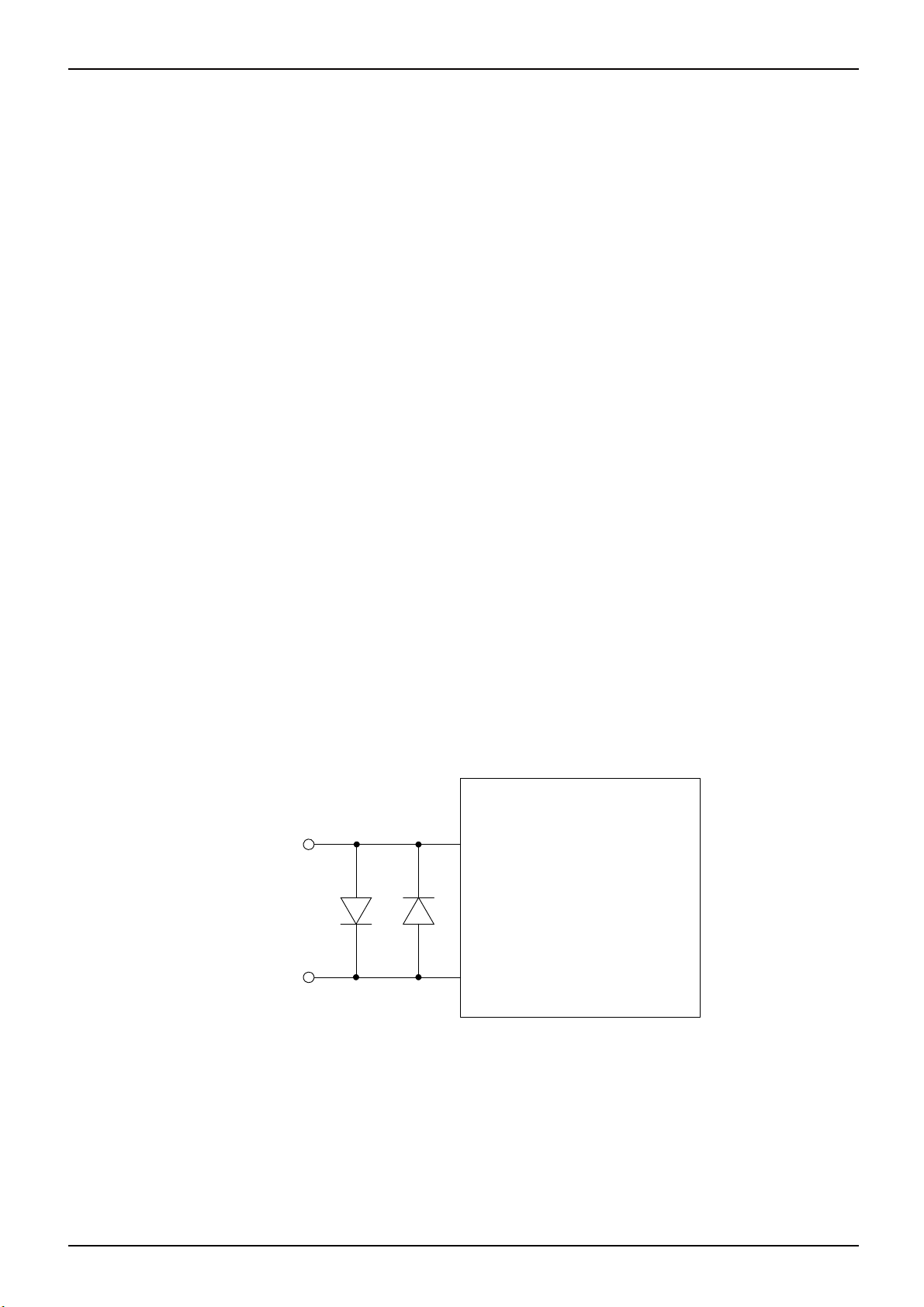
(8) VGND1(31pin), VGND2(1pin) and AGND(9pin) connection
When to float any one of GND pins(VGND1, VGND2 and AGND) during operation, the internal ESD protection diode
Between VGND1, VGND2 and AGND may be damaged by large current surge. If the abnormal design like floating any
one of GND pins is required, it is advisable to connect external diodes between GND pins. The connection detail of
external diodes is illustrated in Fig.7.
AGND
VGND1
VGND2
*
*
* :1SR154-400(ROHM) etc.
Fig.7 External diodes
9pin
31pin
1pin
Technical Note
BH7649KS2
www.rohm.com
11/13
© 2011 ROHM Co., Ltd. All rights reserved.
2011.04 - Rev.

A
BH7649KS2
●Ordering part number
B D 7 6 4 9 K S 2
Technical Note
Part No. Part No.
SQFP-T52
12.0± 0.3
10.0± 0.2
39
40
10.0± 0.2
12.0± 0.3
52
1
1.4± 0.1
0.1± 0.1
0.65
27
13
0.3± 0.1
Package
KS2 : SQFP-T52
Packaging and forming specification
None: Tray
<Tape and Reel information>
Tray (with dry pack)Container
26
14
0.15
0.5
0.125± 0.1
(Unit : mm)
Quantity
Direction of feed
1pin
1000pcs
Direction of product is fixed in a tray
Order quantity needs to be multiple of the minimum quantity.
∗
www.rohm.com
12/12
© 2011 ROHM Co., Ltd. All rights reserved.
2011.04 - Rev.

Notes
No copying or reproduction of this document, in part or in whole, is permitted without the
consent of ROHM Co.,Ltd.
The content specied herein is subject to change for improvement without notice.
The content specied herein is for the purpose of introducing ROHM's products (hereinafter
"Products"). If you wish to use any such Product, please be sure to refer to the specications,
which can be obtained from ROHM upon request.
Examples of application circuits, circuit constants and any other information contained herein
illustrate the standard usage and operations of the Products. The peripheral conditions must
be taken into account when designing circuits for mass production.
Great care was taken in ensuring the accuracy of the information specied in this document.
However, should you incur any damage arising from any inaccuracy or misprint of such
information, ROHM shall bear no responsibility for such damage.
The technical information specied herein is intended only to show the typical functions of and
examples of application circuits for the Products. ROHM does not grant you, explicitly or
implicitly, any license to use or exercise intellectual property or other rights held by ROHM and
other parties. ROHM shall bear no responsibility whatsoever for any dispute arising from the
use of such technical information.
The Products specied in this document are intended to be used with general-use electronic
equipment or devices (such as audio visual equipment, ofce-automation equipment, communication devices, electronic appliances and amusement devices).
The Products specied in this document are not designed to be radiation tolerant.
While ROHM always makes efforts to enhance the quality and reliability of its Products, a
Product may fail or malfunction for a variety of reasons.
Please be sure to implement in your equipment using the Products safety measures to guard
against the possibility of physical injury, re or any other damage caused in the event of the
failure of any Product, such as derating, redundancy, re control and fail-safe designs. ROHM
shall bear no responsibility whatsoever for your use of any Product outside of the prescribed
scope or not in accordance with the instruction manual.
The Products are not designed or manufactured to be used with any equipment, device or
system which requires an extremely high level of reliability the failure or malfunction of which
may result in a direct threat to human life or create a risk of human injury (such as a medical
instrument, transportation equipment, aerospace machinery, nuclear-reactor controller, fuelcontroller or other safety device). ROHM shall bear no responsibility in any way for use of any
of the Products for the above special purposes. If a Product is intended to be used for any
such special purpose, please contact a ROHM sales representative before purchasing.
If you intend to export or ship overseas any Product or technology specied herein that may
be controlled under the Foreign Exchange and the Foreign Trade Law, you will be required to
obtain a license or permit under the Law.
Notice
www.rohm.com
© 2011 ROHM Co., Ltd. All rights reserved.
Thank you for your accessing to ROHM product informations.
More detail product informations and catalogs are available, please contact us.
ROHM Customer Support System
http://www.rohm.com/contact/
R1120
A
 Loading...