

1/4
Structure : Silicon Monolithic Integrated Circuit
Product name : Wide Bandwidth Audio-Video SW for TV
: BH7645KS2
Type
Outer dimensions : Fig.1 SQFP-T52
Block diagram : Fig.2
Features : 1) Video inputs selector : 2-inputs component, 2-inputs Y/C, and 2-inputs composite
2) Component inputs : Correspond to D5 standard
3) Built-in LPF selector(6.75MHz/13.5MHz/30MHz/Through)
4) Built-in Video MUTE function
5) Audio inputs selector : 6-inputs (Lch, Rch)
6) Built-in Power-on MUTE function
2
7) I
C-BUS control
8) Optional Slave address modifications(90H/92H)
2
9) I
C-BUS is compatible with fast mode of Version2.0, but not compatible with Hs mode
10) Built-in detector 3ch(S_SW1/S_SW2/S_SW3)
11) Built-in output port 2ch(PORT1_OUT/PORT2_OUT)
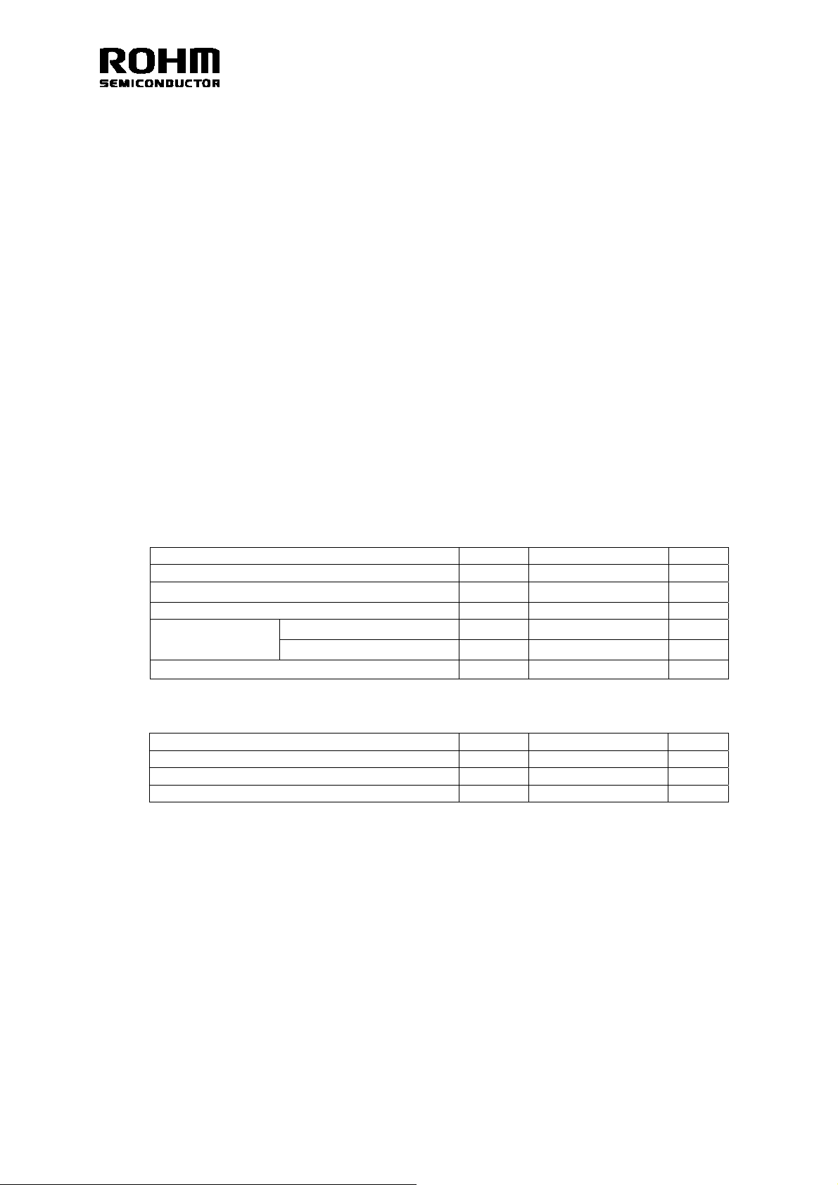
○Absolute Maximum Ratings (Ta=+25℃)
Parameter Symbol Ratings Unit
Supply voltage1 (2pin, 29pin, 33pin, 39pin, 44pin) Vcc1 7 V
Supply voltage2 (12pin) Vcc2 8.8 V
Power dissipation Pd 1300 *1 mW
Input voltage range
Storage temperature range Tstg -55 ~ +125 ℃
VIDEO PART, LOGIC PART V
AUDIO PART V
0 ~ Vcc1+0.2 V
IN1
0 ~ Vcc2+0.2 V
IN2
*1 When mounting on a 70mm×70mm×1.6mm PCB board
Reduced by 13mW/℃ at Ta = +25℃ or higher
○Operating Range
Parameter Symbol Range Unit
Supply voltage1 (2pin, 29pin, 33pin, 39pin, 44pin) Vcc1 +4.5 ~ +5.5 V
Supply voltage2 (12pin) Vcc2 +7.5 ~ +8.5 V
Operating temperature range Topr -40 ~ +85 ℃
* This product is not designed for protection against radioactive rays.
* Note the power supply sequence.
REV. A
2/4
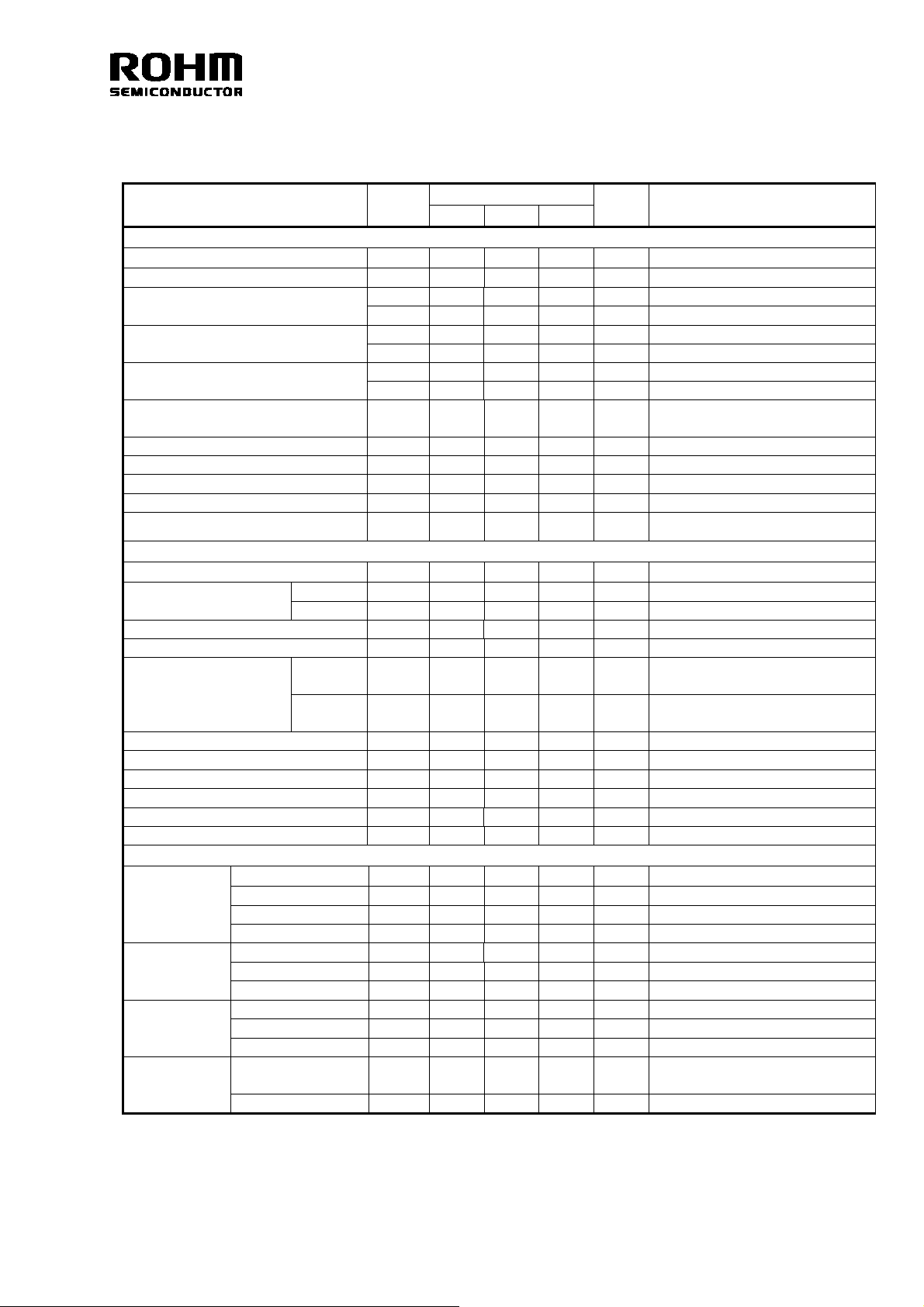
A
○Electrical characteristics (Unless otherwise specified, Ta= 25℃, Vcc1=5.0V, Vcc2=8.0V)
Item Symbol
Min. Typ. Max.
[VIDEO PART]
Circuit current ICCV - 55 80 mA No signal
Voltage gain GVV -0.5 0.0 0.5 dB Vin=1.0Vpp, f=100kHz
Frequency characteristics1
[f=6.75MHz LPF MODE]
Frequency characteristics 2
[f=13.5MHz LPF MODE]
Frequency characteristics 3
[f=30MHz LPF MODE]
Frequency characteristics 4
[f=THROUGH MODE]
Maximum output level VOM
SW crosstalk CTSW
Channel crosstalk CTCH
GF
GF
GF
GF
GF
GF
GF
1-1V
1-2V
2-1V
2-2V
3-1V
3-2V
4-1V
-1.5 0.0 1.0 dB Vin=1.0Vpp, f=6.75MHz/100kHz
-1.5 0.0 1.0 dB Vin=1.0Vpp, f=13.5MHz/100kHz
-1.5 0.0 1.0 dB Vin=1.0Vpp, f=30MHz/100kHz
-3.0 -0.5 2.0 dB Vin=1.0Vpp, f=54MHz/100kHz
V
V
V
MUTE attenuation MTV - -60 -50 dB Vin=1.0Vpp, f=10MHz
Bias input terminal Input impedance ZINV 100 150 - kΩ
[AUDIO PART] (at Gain=0dB)
Circuit current ICCA - 10 15 mA No signal
Voltage gain
0dB GV0A -0.5 0.0 0.5 dB Vin=1.0Vrms, f=1kHz
6dB GV6A 5.5 6.0 6.5 dB Vin=1.0Vrms, f=1kHz
Frequency characteristics GFA -3.0 0.0 3.0 dB Vin=1.0Vrms, f=50kHz/1kHz
Total harmonic distortion THDA - 0.03 0.1 % Vin=1.0Vrms, f=1kHz ※1
0dB VOM0
A
Maximum output level
6dB VOM6
Channel crosstalk CTCH
SW crosstalk CTSW
A
A
A
MUTE attenuation MTA - -100 -85 dB Vin=2.0Vrms, f=1kHz ※1
Remain noise NA - 30 50 uVrms ※1
PSRR PSRR
Input impedance ZINA 100 150 - kΩ
[LOGIC PART etc.]
VIL Vin1L 0 - 1.0 V Low Level input voltage
[SCL]
[SDA]
VIH Vin1H 2.0 - Vcc1 V High Level input voltage
Input bias current IINI2C -10 0 10 uA
SDA output voltage VinL 0 - 0.4 V IL=3.0mA(sink)
VIL Vin2L 0 - 1.0 V Low Level input voltage
[ADR]
[S_SW1]
[S_SW2]
[S_SW3]
[PORT1_OUT]
[PORT2_OUT]
VIH Vin2H 2.0 - Vcc1 V High Level input voltage
Input impedance ZIN
ADR
VIL Vin2L 0 - 1.0 V Low Level input voltage
VIH Vin2H 2.0 - Vcc1 V High Level input voltage
Input impedance ZIN
PORT output
voltage
V
PL
100 150 - kΩ Pull up resistance
SSW
- - 0.5 V I
Leak current IPH - - 5.0 uA Vcc2=8.0V
Limits
Unit Conditions
- -30 -20 dB Vin=1.0Vpp, f=27MHz/100kHz
- -30 -20 dB Vin=1.0Vpp, f=54MHz/100kHz
- -18 -10 dB Vin=1.0Vpp, f=74MHz/100kHz
2.6 3.0 - Vpp f=10kHz, THD=1.0%
- -60 -50 dB Vin=1.0Vpp, f=10MHz
- -60 -50 dB Vin=1.0Vpp, f=10MHz
2.0 2.4 - Vrms
2.0 2.4 - Vrms
Maximum value of distortion<0.3%
Maximum value of distortion<0.3%
- -100 -85 dB Vin=2.0Vrms, f=1kHz ※1
- -100 -85 dB Vin=2.0Vrms, f=1kHz ※1
- -45 -38 dB ※2
70 100 130 kΩ
※1 400HzHPF + 30kHzLPF ON
※2 Vin=0.3Vpp, f=100Hz at VCC, 30kHzLPF ON
f=1kHz ※1
f=1kHz ※1
=2.5mA
L
REV. A

3/4
イ
系
W
W
○Physical dimensions ○Block diagram
CY/Y/
Vcc5V RGBout
PORT1 OUT
CYin1
ADDRESS
CYin2
PBin1
TEST1
PBin2
S SW3
S SW2
PRin1
S SW1
PRin2
40
41
42
43
44
45
46
47
48
49
50
51
52
Clamp
Clamp
1 2 3 4 5 6 7 8 9 10 11
Y1in1
: テレビ用Hd 対応AVス
BH7645KS2
:
BH7645KS2
: 1) ビデオ入力セレクタ:
ネント 入力2系統、Y/C 入力2
Lot No.
Fig.1 SQFP-T52 ( UNIT:mm )
Vcc5V Video IN2
Bias
Bias
S SW
Bias
Bias
CVBSout1
PBout1
GND RGBout
PR/Cout1
DVcc5V
SDA
SCL
Gain_SEL
0/6dB
0/6dB
Bias
C1in1
DGND
P-on
Mute
P-on
Mute
Audio_SW
Mute
6in-1out
Mute
Vref AU
GND
I2C LOGIC
0dB
0dB
CY_S
6.75M/13.5M/
Mute
30M/Through
PB_S
Mute
PR_SW
Mute
Y_SW
Clamp
Clamp
Clamp
CVBS1
Vcc5V Video IN1
Y1in2
Vref Video
LPF1
LPF2
6.75M/13.5M/
30M/Through
LPF3
6.75M/13.5M/
30M/Through
Clamp
GND
0dB
C_SW
Bias
CVBS2
GND Video IN
Lout
12 13
Vcc8V AU
Rout
2728
GND AU
26
R6in
25
L6in
24
R5in
23
L5in
22
R4in
21
L4in
20
R3in
19
L3in
18
R2in
17
L2in
16
R1in
15
L1in
14
PORT2 OUT
Vcc5V AU
2930 31 32 33 34 3536373839
C1in2
Fig.2 Block diagram
Pin number Pin name Pin number Pin name Pin number Pin name Pin number Pin name
1 Y1in1 14 L1in 27 Rout 40 PORT1 OUT
2 Vcc5V Video IN1 15 R1in 28 Lout 41 CYin1
3 CVBS1 16 L2in 29 Vcc5V AU 42 ADDRESS
4 Vref Video 17 R2in 30 DGND 43 CYin2
5 Y1in2 18 L3in 31 SCL 44 Vcc5V Video IN2
6 GND 19 R3in 32 SDA 45 PBin1
7 CVBS2 20 L4in 33 DVcc5V 46 TEST1
8 GND Video IN 21 R4in 34 PR/Cout1 47 PBin2
9 C1in1 22 L5in 35 GND RGBout 48 S SW3
10 Vref AU 23 R5in 36 PBout1 49 S SW2
11 C1in2 24 L6in 37 GND 50 PRin1
12 Vcc8V AU 25 R6in 38 CY/Y/CVBSout1 51 S SW1
13 PORT2 OUT 26 GND AU 39 Vcc5V RGBout 52 PRin2
Pin number and Pin name
○
REV. A

4/4
○Cautions for use
(1) Absolute maximum ratings
If the absolute maximum ratings for applied voltage and/or operation temperature are exceeded, LSI damage may result.
Therefore, do not apply voltage or use in a temperature that exceeds these absolute maximum ratings.
If it is possible that absolute maximum ratings will be exceeded, use a physical safety device such as a fuse and make
sure that no conditions that might exceed the absolute maximum ratings will be applied to the LSI IC.
(2) Power supply line
Design PCB pattern to provide low impedance for the wiring between the power supply and the GND lines.
In this regard, for the digital block power supply and the analog block power supply, even though these power supplies
has the same level of potential, separate the power supply pattern for the digital block from that for the analog block,
thus suppressing the diffraction of digital noises to the analog block power supply resulting from impedance common to
the wiring patterns. For the GND line, give consideration to design the patterns in a similar manner.
Furthermore, for all power supply terminals to ICs, mount a capacitor between the power supply and the GND terminal.
At the same time, in order to use an electrolytic capacitor, thoroughly check to be sure the characteristics of the
capacitor to be used present no problem including the occurrence of capacity dropout at a low temperature, thus
determining the constant.
(3) GND potential
Regardless of the operation mode, the voltage of the GND pin should be at least the minimum voltage.
Actually check whether or not the voltage at each pin, including transient phenomena, is less than the GND pin voltage.
(4) Thermal design
The thermal design should be done using an ample margin that takes into consideration the allowable dissipation under
actual use conditions.
(5) Shorts between pins and mounting errors
When mounting LSI ICs onto the circuit board, make sure each LSI's orientation and position is correct.
The ICs may become damaged if they are not mounted correctly when the power is turned on.
Similarly, damage may also result if a short occurs, such as when a foreign object is positioned between pins in an IC,
or between a pin and a power supply or GND connection.
(6) Operation in strong electromagnetic field
When used within a strong electromagnetic field, evaluate carefully to avoid the risk of operation faults.
(7) Power supply sequence
[Power-up sequence]
Supply voltage1 (Vcc1 : 2pin, 29pin, 33pin, 39pin, 44pin) must be powered up before or at the same time as the
supply voltage2 (Vcc2 : 12pin).
[Power-down sequence]
Supply voltage2 (Vcc2 : 12pin) must be powered up before or at the same time as the supply voltage1(Vcc1 : 2pin,
29pin, 33pin, 39pin, 44pin).
REV. A

Notes
No copying or reproduction of this document, in par t or in whole, is permitted without the
consent of ROHM Co.,Ltd.
The content specied herein is subject to change for improvement without notice.
The content specied herein is for the purpose of introducing ROHM's products (hereinafter
"Products"). If you wish to use any such Product, please be sure to refer to the specications,
which can be obtained from ROHM upon request.
Examples of application circuits, circuit constants and any other information contained herein
illustrate the standard usage and operations of the Products. The peripheral conditions must
be taken into account when designing circuits for mass production.
Great care was taken in ensuring the accuracy of the information specied in this document.
However, should you incur any damage arising from any inaccuracy or misprint of such
information, ROHM shall bear no responsibility for such damage.
The technical information specied herein is intended only to show the typical functions of and
examples of application circuits for the Products. ROHM does not grant you, explicitly or
implicitly, any license to use or exercise intellectual property or other rights held by ROHM and
other parties. ROHM shall bear no responsibility whatsoever for any dispute arising from the
use of such technical information.
Notice
The Products specied in this document are intended to be used with general-use electronic
equipment or devices (such as audio visual equipment, ofce-automation equipment, communication devices, electronic appliances and amusement devices).
The Products specied in this document are not designed to be radiation tolerant.
While ROHM always makes efforts to enhance the quality and reliability of its Products, a
Product may fail or malfunction for a variety of reasons.
Please be sure to implement in your equipment using the Products safety measures to guard
against the possibility of physical injury, re or any other damage caused in the event of the
failure of any Product, such as derating, redundancy, re control and fail-safe designs. ROHM
shall bear no responsibility whatsoever for your use of any Product outside of the prescribed
scope or not in accordance with the instruction manual.
The Products are not designed or manufactured to be used with any equipment, device or
system which requires an extremely high level of reliability the failure or malfunction of which
may result in a direct threat to human life or create a risk of human injur y (such as a medical
instrument, transportation equipment, aerospace machinery, nuclear-reactor controller, fuelcontroller or other safety device). ROHM shall bear no responsibility in any way for use of any
of the Products for the above special purposes. If a Product is intended to be used for any
such special purpose, please contact a ROHM sales representative before purchasing.
If you intend to export or ship overseas any Product or technology specied herein that may
be controlled under the Foreign Exchange and the Foreign Trade Law, you will be required to
obtain a license or permit under the Law.
Thank you for your accessing to ROHM product informations.
More detail product informations and catalogs are available, please contact us.
ROHM Customer Support System
www.rohm.com
© 2010 ROHM Co., Ltd. All rights reserved.
http://www.rohm.com/contact/
R1010
A
 Loading...