

Page 1

High-performance video signal Switcher Series
Video Drivers with Built-in
Low Voltage operation Single Video Switchers
High-performance System video Driver Series
Video Drivers with Built-in
Input Selection SW
BH76330FVM, BH76331FVM, BH76360FV, BH76361FV
High-performance video signal Switcher Series
Wide Band
Low Voltage operation Single Video Switchers
BH76332FVM, BH76333FVM, BH76362FV, BH76363FV
INDEX
Video Drivers with Built-in
Low Voltage operation Single Video Switchers
BH76330FVM (3input 1output Video Switch)・・・・・・P2
BH76331FVM (3input 1output Video Switch)・・・・・・P2
No.09065EAT01
BH76360FV (6input 1output Video Switch)・・・・・・P17
BH76361FV (6input 1output Video Switch)・・・・・・P17
Wide Band
Low Voltage operation Single Video Switchers
BH76332FVM (3input 1output Video Switch)・・・・・・P2
BH76333FVM (3input 1output Video Switch)・・・・・・P2
BH76362FV (6input 1output Video Switch)・・・・・・P17
BH76363FV (6input 1output Video Switch)・・・・・・P17
www.rohm.com
© 2009 ROHM Co., Ltd. All rights reserved.
1/32
2009.04 - Rev.A
Page 2
BH76330FVM, BH76331FVM, BH76360FV, BH76361FV,
BH76332FVM, BH76333FVM, BH76362FV, BH76363FV
Technical Note
Line-up of products with built-in video amplifier and video driver
3-input, 1-output video switch
BH76330FVM, BH76331FVM, BH76332FVM, BH76333FVM
● General
BH76330FVM, BH76331FVM, BH76332FVM, and BH76333FVM are video signal switching ICs, each with three inputs and
one circuit input, which feature wide dynamic range and frequency response. Since these ICs can be used with low voltage
starting at VCC = 2.8 V, they are applicable not only in stationary devices but also in mobile devices.
This product line-up supports a broad range of input signals, depending on whether or not a 6-dB video amplifier and video
driver are included and what combination of sync tip clamp type and bias (resistor termination) type inputs are used.
● Features
1) Able to use a wide range of power supply voltage, from 2.8 V to 5.5 V
2) Wide output dynamic range
3) Excellent frequency response
(BH76330FVM and BH76331FVM: 100 kHz/10 MHz 0 dB [Typ.], BH76332FVM and BH76333FVM: 100 kHz/30
MHz 0 dB [Typ.])
4) No crosstalk between channels (Typ. -65 dB, f = 4.43 MHz)
5) Built-in standby function, circuit current during standby is 0 µA (Typ.)
6) Sync tip clamp input (BH76330FVM, BH76332FVM)
7) Bias input (Zin = 150 k) (BH76331FVM, BH76333FVM)
8) 6-dB amp and 75 driver are built in (BH76330FVM, BH76331FVM)
9) Enables two load drivers [when using output coupling capacitor] (BH76330FVM, BH76331FVM)
10) Able to be used without output coupling capacitor (BH76330FVM)
11) MSOP8 compact package
● Applications
Input switching in car navigation systems, TVs, DVD systems, etc.
● Line-up
BH76330FVM BH76331FVM BH76332FVM BH76333FVM
Supply voltage 2.8 V to 5.5 V
Amp gain 6 dB -0.1 dB
Video driver Included -
Frequency response 100 kHz/10 MHz, 0 dB (Typ.) 100 kHz/30 MHz, 0 dB (Typ.)
Input type
● Absolute maximum ratings (Ta = 25℃)
Parameter Symbol Limits Unit
Supply voltage VCC 7.0 V
Power dissipation Pd 470 *1 mW
Input voltage range VIN 0 to VCC+0.2 V
Operating temperature
range
Storage temperature
range
● Operation range (Ta = 25℃)
Parameter Symbol Min. Typ. Max Unit
Supply voltage VCC 2.8 5.0 5.5 V
Sync tip
clamp
*1 When used while Ta = 25℃, 4.7 mW is dissipated per 1℃
Mounted on 70 mm x 70 mm x 1.6 mm glass epoxy board
Bias
(Zin = 150 k)
Topr
Ts tg
Sync tip
clamp
-40 to +85 ℃
-55 to +125 ℃
(Zin = 150 k)
Bias
www.rohm.com
© 2009 ROHM Co., Ltd. All rights reserved.
2/32
2009.04 - Rev.A
Page 3
BH76330FVM, BH76331FVM, BH76360FV, BH76361FV,
BH76332FVM, BH76333FVM, BH76362FV, BH76363FV
● Electrical characteristics 1 (unless otherwise specified, Ta = 25℃, VCC = 5 V)
Parameter Symbol
76330 76331 76332 76333
Typ.
Unit Conditions
Circuit current 1 ICC1 10 9 mA When no signal
Circuit current 2 ICC2 0.0 µA During standby
Circuit current 3
ICC3-1 11 10
ICC3-2 17 -
During output of color bar signal
mA
During output of color bar signal
(no C in output)
Maximum output level VOM 4.6 3.8 3.4 Vpp f = 10 kHz, THD = 1%
Voltage gain GV 6.0 -0.1 dB Vin = 1.0 Vpp, f = 100 kHz
G
0 - dB Vin = 1.0 Vpp, f = 10 MHz/100 kHz
Frequency response
Crosstalk between
channels
F1
GF2 - 0 dB Vin = 1.0 Vpp, f = 30 MHz/100 kHz
CT -65 dB Vin = 1.0 Vpp, f = 4.43 MHz
Mute attenuation MT -65 dB Vin = 1.0 Vpp, f = 4.43 MHz
CTL pin switch level
CTL pin inflow current I
THH 1.2
V
VTHL 0.45
50
THH
V High level threshold voltage
Min
V Low level threshold voltage
Max
µA CTL pin = 2.0 V applied
Max
Input impedance Zin - 150 - 150 k
Differential gain DG 0.3 %
DP-1 0.7 0.3
Differential phase
DP-2 0.0 -
Y-related S/N SNY +75 +78 dB
C-related S/N [AM] SNCA +75
C-related S/N [PM] SNCP +65
Vin = 1.0 Vpp
Standard stair step signal
deg.
Same condition as above
(no C in output)
Vin = 1.0 Vpp, bandwidth: 100 k to 6 MHz
100% white video signal
Vin = 1.0 Vpp, bandwidth: 100 to 500 kHz
dB
100% chroma voltage signal
● Electrical characteristics 2 (unless otherwise specified, Ta = 25℃, VCC = 3 V)
Parameter Symbol
76330 76331 76332 76333
Typ.
Unit Conditions
Circuit current 1 ICC1 8.5 8.0 mA When no signal
Circuit current 2 ICC2 0.0 µA During standby
ICC3-1 9.5 9.0 mA During output of color bar signal
Circuit current 3
ICC3-2 15.5 -
During output of color bar signal
(no C in output)
Maximum output level VOM 2.7 2.8 1.8 1.9 Vpp f = 10 kHz, THD = 1%
Voltage gain GV 6.0 -0.1 dB Vin = 1.0 Vpp, f = 100 kHz
G
0 - dB Vin = 1.0 Vpp, f = 10 MHz/100 kHz
Frequency response
Crosstalk between
channels
F1
GF2 - 0 dB Vin = 1.0 Vpp, f = 30 MHz/100 kHz
-65 dB Vin = 1.0 Vpp, f = 4.43 MHz
C
T
Mute attenuation MT -65 dB Vin = 1.0 Vpp, f = 4.43 MHz
CTL pin switch level
CTL pin inflow current I
THH 1.2
V
VTHL 0.45
50
THH
V High level threshold voltage
Min
V Low level threshold voltage
Max
µA CTL pin = 2.0 V applied
Max
Input impedance Zin - 150 150 k
Differential gain DG 0.3 0.7 0.3 %
D
-1 1.0 0.3
P
Differential phase
DP-2 0.5 -
Y-related S/N SNY +75 +78 dB
C-related S/N [AM] SNCA +75 dB
C-related S/N [PM] SNCP +65 dB
(Note) Re: ICC3, VOM, GV, GF, CT, MT, DG, DP, SNY, SNCA, and SNCP parameters
BH76330FVM and BH76331FVM: RL = 150
BH76332FVM and BH76333FVM: RL = 10 k
Vin = 1.0 Vpp
Standard stair step signal
deg.
Same condition as above
(no C in output)
Vin = 1.0 Vpp, bandwidth: 100 k to 6 MHz
100% white video signal
Vin = 1.0 Vpp, bandwidth: 100 to 500 kHz
100% chroma video signal
Technical Note
www.rohm.com
© 2009 ROHM Co., Ltd. All rights reserved.
3/32
2009.04 - Rev.A
Page 4
BH76330FVM, BH76331FVM, BH76360FV, BH76361FV,
BH76332FVM, BH76333FVM, BH76362FV, BH76363FV
● Control pin settings
CTL
A B
STBY L(OPEN) L(OPEN)
IN1 L(OPEN) H
IN2 H L(OPEN)
IN3 H H
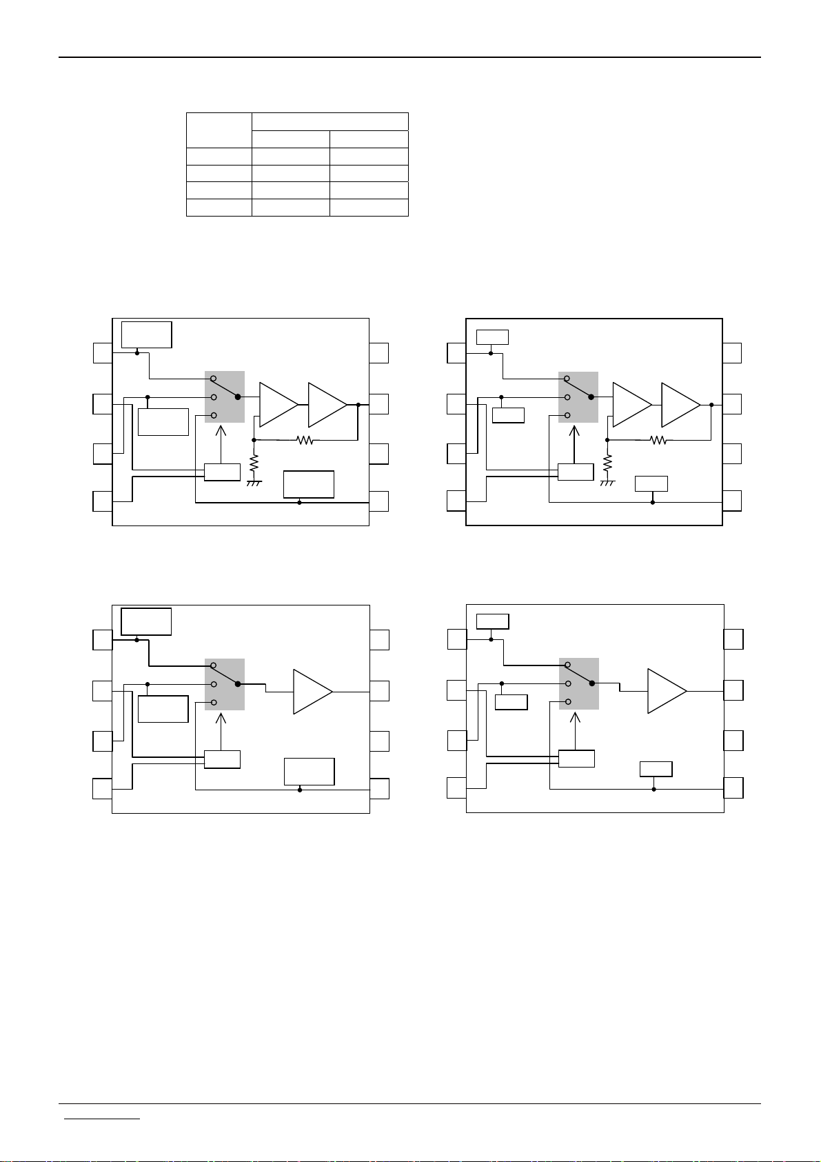
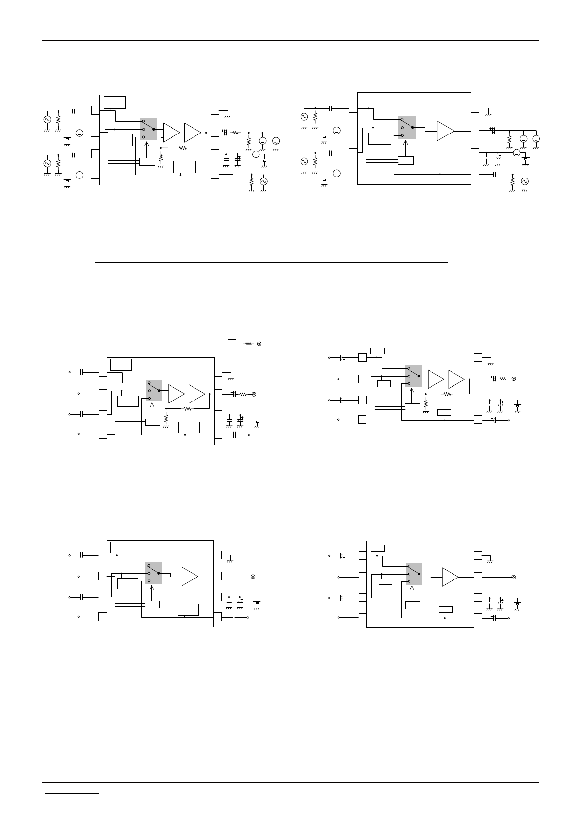
● Block diagram
CTLA
CTLB
CTLA
CTLB
Sync_Tip
IN1
Clamp
1
6dB
75Ω
IN2
2
Sync_Tip
Clamp
3 6
logic
Sync_Tip
Clamp
4 5
Fig.1 BH76330FV Fig.2 BH76331FV
Sync_Tip
IN1
Clamp
1
0dB
IN2
2
Sync_Tip
Clamp
3 6
logic
Sync_Tip
Clamp
4 5
Fig. 3 BH76332FV Fig. 4 BH76333FV
Technical Note
GND
8
OUT
7
VCC
IN3
GND
8
OUT
7
VCC
IN3
CTLA
CTLB
CTLA
CTLB
BIAS
IN1
IN2
1
2
BIAS
6dB
75Ω
GND
8
OUT
7
VCC
36
logic
BIAS
IN3
4 5
BIAS
IN1
IN2
1
2
BIAS
0dB
GND
8
OUT
7
VCC
36
logic
BIAS
IN3
4 5
www.rohm.com
© 2009 ROHM Co., Ltd. All rights reserved.
4/32
2009.04 - Rev.A
Page 5
BH76330FVM, BH76331FVM, BH76360FV, BH76361FV,
BH76332FVM, BH76333FVM, BH76362FV, BH76363FV
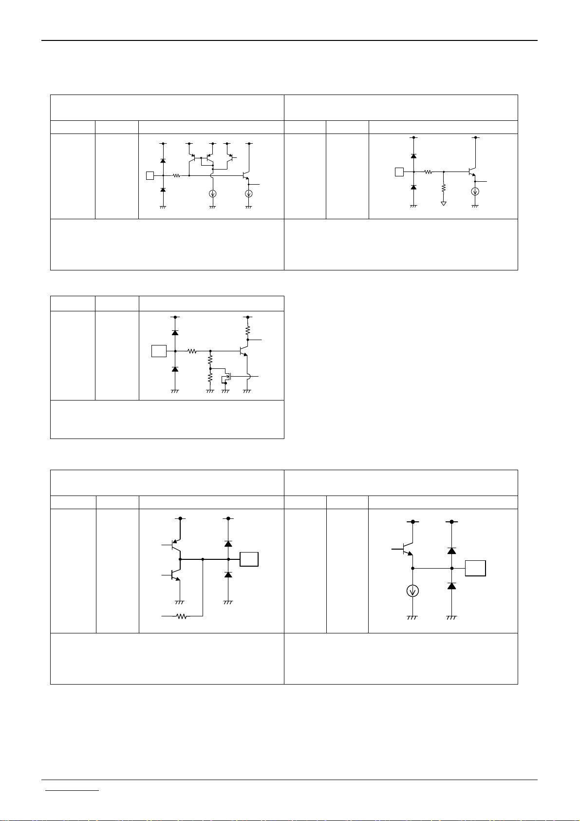
● I/O equivalent circuit diagrams
Input pins
Sync tip clamp input
BH76330FVM/BH76332FVM
Pin No. Name Equivalent circuit Pin No. Name Equivalent circuit
Bias input
BH76331FVM/BH76333FVM
Technical Note
1
3
5
IN1
IN2
IN3
IN
100Ω
Video signal input pin is used for sync tip clamp input.
・DC potential
BH76330FVM: 1.5 V BH76332FVM: 1.0 V
Control pins
Pin No. Name Equivalent circuit
200k
Ω
2
4
CTLA
CTLB
CTL
50kΩ
250kΩ
200kΩ
Switches operation mode [active or standby] and input
pin.
Threshold level is 0.45 V to 1.2 V.
Output pin
1
3
5
IN1
IN2
IN3
IN
100Ω
150kΩ
Video signal input pin is used for bias type input. Input
impedance is 150 k.
・DC potential
BH76331FVM: 3.1 V BH76333FVM: 2.5 V
With video driver
BH76330FVM/BH76331FVM
Without video driver
BH76332FVM/BH76333FVM
Pin No. Name Equivalent circuit Pin No. Name
OUT
7 OUT
14kΩ
Video signal output pin. Able to drive loads up to 75
(dual drive).
・DC potential
BH76330FVM: 0.16 V BH76331FVM: 2.5 V
7 OUT
Video signal output pin.
・DC potential
BH76332FVM: 0.3 V BH76333FVM: 1.8 V
OUT
3.0mA
Note 1) The above DC potential is only when VCC = 5 V. This value is a reference value and is not guaranteed.
Note 2) Numerical values shown in these figures are design values, and compliance to standards is not guaranteed.
www.rohm.com
© 2009 ROHM Co., Ltd. All rights reserved.
5/32
2009.04 - Rev.A
Page 6
BH76330FVM, BH76331FVM, BH76360FV, BH76361FV,
BH76332FVM, BH76333FVM, BH76362FV, BH76363FV
● Test Circuit Diagrams
VCC
Sync_Tip
IN1
0.01μF
50Ω
0.01μF
50Ω
Clamp
1
CTLA
A
2
Sync_Tip
Clamp
IN2
36
CTLB
A
4 5
logic
0.01μF
50Ω
0.01μF
50Ω
Sync_Tip
IN1
Clamp
1
CTLA
A
2
Sync_Tip
Clamp
IN2
3 6
CTLB
A
4 5
logic
6dB
Sync_Tip
Clamp
75Ω
GND
8
OUT
7
VCC
IN3
10μF
0.01μF
0.01μF
75Ω
75Ω
50Ω
10μF
V V
A
Fig. 5 BH76330FV/BH76331FV Test Circuit Diagram
Fig. 6 BH76332FV/BH76333FV Test Circuit Diagram
Test circuit diagrams are used for shipment inspections, and differ from application circuits.
● Application circuit examples
GND
8
OUT
7
VCC
IN3
470μF
0.1μF
When used without
output capacitor
7
75Ω
75Ω
47μF
VIDEO_IN
0.1μF
VIDEO_OUT
VIDEO_OUT
VCC
BIAS
VIDEO_IN
VIDEO_IN
IN1
1
4.7μF
CTLA
2
BIAS
IN2
36
4.7μF
CTLB
4 5
logic
VIDEO_IN
VIDEO_IN
Sync_Tip
IN1
Clamp
1
0.1μF
CTLA
2
Sync_Tip
Clamp
IN2
3 6
0.1μF
CTLB
4 5
logic
6dB
75Ω
Sync_Tip
Clamp
Fig. 7 BH76330FV
Fig. 8 BH76331FV
VIDEO_IN
VIDEO_IN
Sync_Tip
IN1
Clamp
1
0.1μF
CTLA
2
Sync_Tip
Clamp
IN2
3 6
0.1μF
CTLB
4 5
logic
0dB
Sync_Tip
Clamp
GND
8
OUT
7
VCC
IN3
0.1μF
0.1μF
47μF
VIDEO_OUT
VCC
VIDEO_IN
VIDEO_IN
VIDEO_IN
BIAS
IN1
1
4.7μF
CTLA
2
BIAS
IN2
36
4.7μF
CTLB
4 5
logic
Fig. 9 BH76332FV
Fig. 10 BH76333FV
See pages 6/16 to 10/16 for description of how to determine the capacity of I/O coupling capacitors.
6dB
Technical Note
GND
8
0dB
75Ω
OUT
7
VCC
IN3
OUT
OUT
GND
VCC
GND
VCC
8
7
IN3
8
7
IN3
0dB
Sync_Tip
Clamp
BIAS
BIAS
10μF
0.01μF
0.01μF
470μF
0.1μF
0.1μF
4.7μF
4.7μF
10kΩ
10μF
50Ω
75Ω
47μF
47μF
V V
A
VCC
VIDEO_OUT
VCC
VIDEO_IN
VIDEO_OUT
VCC
VIDEO_IN
www.rohm.com
© 2009 ROHM Co., Ltd. All rights reserved.
6/32
2009.04 - Rev.A
Page 7
BH76330FVM, BH76331FVM, BH76360FV, BH76361FV,
BH76332FVM, BH76333FVM, BH76362FV, BH76363FV
● Cautions for selection and use of application parts
When using this IC by itself ①
Input type
Sync_Tip_Clamp 10 M 0.1 µF
Bias 150 k 4.7 µF
Input impedance
Zin
Capacity of input coupling
capacitor (recommended
value)
Capacity of output coupling
capacitor (recommended
value)
470 µF to 1000 µF
Technical Note
Method for determining capacity of input coupling capacitor
The HPF is comprised of an input coupling capacitor and the internal input impedance Zin of the IC. Since the fc value of this HPF is
determined using the following equation (a), the above recommended capacity for the input capacitor is derived. Usually, the cutoff
frequency fc is several Hz.
fc = 1 / (2π × C × Zin)・・・・(a)
When evaluating the sag characteristics and determining the capacity of the capacitor during video signal input, a horizontal stripe signal
called "H bar" (shown in Fig. 10) is suitable, and this type of signal is used instead of a color bar signal to evaluate characteristics and
determine capacity.
Method for determining capacity of output coupling capacitor
The output pins of models with a 75 driver [BH76330FVM and BH76331FVM] have an HPF comprised of an output coupling capacitor and
load resistance R
approximately 470 µF to 1000 µF.
As for models without the 75 driver, an HPF is similarly comprised using the capacity of the output coupling capacitor and the input
impedance of the IC connected at the next stage, and the capacitance required for the output coupling capacitor should be estimated using
equation (a).
Fig.11 Example of Screen with Obvious Sag (H-bar Signal)
(= 150). When fc is set to approximately 1 Hz or 2 Hz, the capacity of the output coupling capacitor needs to be
L
When this IC is used as a standalone device ②
In models that include a 75 driver [BH76330FVM and BH76331FVM], up to two monitors (loads) can be connected (a connection example
is shown in Fig. 12). When there are multiple loads, the number of output coupling capacitors must be increased or a larger capacitance
must be used, based on the table shown below.
470μF
OUT
7
monitor
75Ω
75Ω
OUT
(470×2)μF
7
75Ω
monitor
75Ω
75Ω
monitor
75Ω
470μF
75Ω
monitor
75Ω
When this IC is used as a standalone device ③
The BH76330FVM is the only model that can be used without an output coupling capacitor.
This use method not only enables reductions in board space and part-related costs, but it is able to improve the sag characteristics by
improving low-range frequency response. However, when the output coupling capacitor is omitted, a direct current flows to the connected
set, so the specifications of the connected set should be noted carefully before starting use.
Note also that only one load can be connected when the output coupling capacitor is omitted.
Fig. 12 (a) Application Circuit Example 1 (Two Drives) Fig. 12 (b) Application Circuit Example 2 (Two Drives)
Application circuit example No. of output capacitors Capacitance per output capacitor (recommended values)
Fig. 12 (a) No. of drives required 470 µF to 1000 µF (same as with one drive)
Fig. 12 (b) 1 (No. of drive × 470 µF to 1000) uF
BH76330FV
OUT
monitor
7
75Ω
75Ω
Voltage at output ≒0.16V
When this voltage load resistance is applied,
a direct current is generated.
www.rohm.com
© 2009 ROHM Co., Ltd. All rights reserved.
Fig.13 Application Example without Output Coupling Capacitor
7/32
2009.04 - Rev.A
Page 8
BH76330FVM, BH76331FVM, BH76360FV, BH76361FV,
yp
)
BH76332FVM, BH76333FVM, BH76362FV, BH76363FV
When using several of these ICs ①
When several of these ICs are used, it enables applications in which separate images are output to the car navigation system's front and
rear monitors.
Technical Note
VIDEO IN
VIDEO IN
VIDEO IN
IN1
1
IN2
3
IN3
5
Clamp
/Bias
Clamp
/Bias
Clamp
/Bias
7
OUT
470μF
75Ω
Front monitor
75Ω
IN1
IN2
IN3
1
3
5
Clamp
/Bias
Clamp
/Bias
Clamp
/Bias
7
OUT
470μF
75Ω
Rear monitor
75Ω
When several ICs are used at the same time, the number of parallel connections of input impedance equals the number of ICs being used,
which reduces the input impedance. This also raises the fc value of the HPF formed at the input pin block, so the capacitance of the input
coupling capacitor must be increased according to equation (a). The recommended values for calculation results are listed in the table
below.
When a clamp is used as the input type, the original input impedance becomes much greater, and if two or three are used at the same time
there is no need to change the capacitance of the input coupling capacitor.
Fig.14 Application Example when Using Several ICs
Capacitance of input
coupling capacitor
(recommended values)
Input type Input impedance per IC
Sync_Tip_Clamp Approx. 10 M
Bias 150 k
Number of ICs
used
Tota l
input impedance
2 Approx. 5 M 0.1 µF
3 Approx. 3 M 0.1 µF
2 75 k 6.8 µF~
3 50 k 10 µF~
When using several of these ICs ②
When three bias input type models (BH76331FVM or BH76333FVM) are used in parallel, they can be used for RGB signal switching
applications. Likewise, when one clamp input type model (BH76330FVM or BH76332FVM) is connected in parallel with two bias input type
models (a total of three ICs used in parallel), they can be used for component signal switching applications. The same method can be used
to determine the capacitance of I/O coupling capacitors of these applications.
VIDEO IN[R1]
4.7μF
VIDEO IN[R2]
4.7μF
VIDEO IN[R3]
4.7μF
VIDEO IN[G1]
4.7μF
VIDEO IN[G2]
4.7μF
VIDEO IN[G3]
4.7μF
Bias
IN1
1
Bias
IN2
3
Bias
IN3
5
Bias
IN1
1
Bias
IN2
3
Bias
IN3
5
BH76331FV
or BH76333FV
BH76331FV
or BH76333FV
VIDEO IN[B1]
4.7μF
VIDEO IN[B2]
4.7μF
VIDEO IN[B3]
4.7μF
Bias
IN1
1
Bias
IN2
3
Bias
IN3
5
BH76331FV
or BH76333FV
Fig. 15 (a). RGB Signal Switching Application Example
(using three bias input type models in parallel)
www.rohm.com
© 2009 ROHM Co., Ltd. All rights reserved.
OUT
7
OUT
7
OUT
7
SW select
R_OUT
G_OUT
B_OUT
VIDEO IN[Py1]
VIDEO IN[Py2]
VIDEO IN[Py3]
VIDEO IN[Pb1]
VIDEO IN[Pb2]
VIDEO IN[Pb3]
VIDEO IN[Pr1]
VIDEO IN[Pr2]
VIDEO IN[Pr3]
Fig. 15 (b). Component Signal Switching Application Example
(using one clamp input type model and two bias input
e models in parallel
t
8/32
0.1uF
0.1uF
0.1uF
4.7uF
4.7uF
4.7uF
4.7uF
4.7uF
4.7uF
Clamp
IN1
1
Clamp
IN2
3
Clamp
IN3
5
Bias
IN1
1
Bias
IN2
3
Bias
IN3
5
Bias
IN1
1
Bias
IN2
3
Bias
IN3
5
BH76330FV
or BH76332FV
OUT
7
BH76331FV
or BH76333FV
OUT
7
BH76331FV
or BH76333FV
OUT
7
Py_OUT
Pb_OUT
Pr_OUT
SW select
2009.04 - Rev.A
Page 9
BH76330FVM, BH76331FVM, BH76360FV, BH76361FV,
k
(
)
y
BH76332FVM, BH76333FVM, BH76362FV, BH76363FV
Technical Note
● Cautions for use
1. The numerical values and data shown here are typical design values, not guaranteed values.
2. The application circuit examples show recommended circuits, but characteristics should be checked carefully before using
these circuits. If any external part constants are modified before use, factors such as variation in all external parts and
ROHM LSI ICs, including not only static characteristics but also transient characteristics, should be fully considered to set
an ample margin.
3. Absolute maximum ratings
If the absolute maximum ratings for applied voltage and/or operation temperature are exceeded, LSI damage may result.
Therefore, do not apply voltage or use in a temperature that exceeds these absolute maximum ratings. If it is possible that
absolute maximum ratings will be exceeded, use a physical safety device such as a fuse and make sure that no conditions
that might exceed the absolute maximum ratings will be applied to the LSI IC.
4. GND potential
Regardless of the operation mode, the voltage of the GND pin should be at least the minimum voltage. Actually check
whether or not the voltage at each pin, including transient phenomena, is less than the GND pin voltage.
5. Thermal design
The thermal design should be done using an ample margin that takes into consideration the allowable dissipation under
actual use conditions.
6. Shorts between pins and mounting errors
When mounting LSI ICs onto the circuit board, make sure each LSI's orientation and position is correct. The ICs may
become damaged if they are not mounted correctly when the power is turned on. Similarly, damage may also result if a
short occurs, such as when a foreign object is positioned between pins in an IC, or between a pin and a power supply or
GND connection.
7. Operation in strong electromagnetic field
When used within a strong electromagnetic field, evaluate carefully to avoid the risk of operation faults.
8. Place the power supply's decoupling capacitor as close as possible to the VCC pin (PIN 6) and GND pin (PIN 8).
9. With a clamp input type model (BH76330FVM or BH76332FVM), if any unused input pins are left open they will oscillate, so
unused input pins should instead be connected to GND via a capacitor or else directly connected to VCC.
10. With models that do not include a 75
driver (BH76332FVM or BH76333FVM), in some cases the capacitance added to the
set board may cause the peak frequency response to occur at a high frequency. To lower the peak frequency, connect in
series resistors having resistance of several dozen
OUT
to several hundred as close as possible to the output pin.
Output pin
7
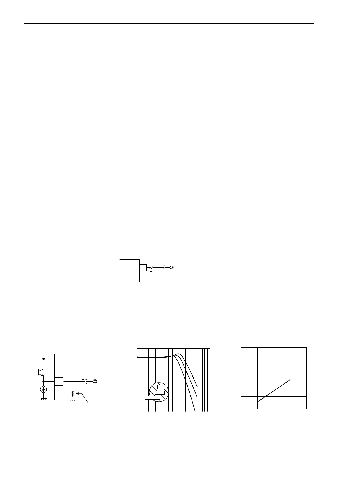
Fig.16 Positions where Resistors are Inserted to Lower Peak Frequency Response in BH76332FV or BH76333FV
Resistors (several dozen Ωto
several hundre dΩ) to lower pea
frequency
11. Frequency response in models that do not include a 75-
driver (BH76332FVM and BH76333FVM) was measured as 100
kH/30 MHz: 0 dB (Typ.) in the application circuit examples (shown in Fig. 9 and Fig. 10), and when resistance of about 1 or
2 k
is applied from the IC's output pin to GND, this frequency response can be improved (the lower limit of the applied
resistance should be 1 k
). In such cases, gain is reduced, since the output voltage is divided by the added resistance
and the output resistance of the IC.
1
OUT
7
3mA
Resistance to improve frequenc
response (R: 1-2 kΩ)
(a) Resistor insertion points
(b) Frequency response changes when resistance is inserted
Other constants are as in application examples (Figs. 9 & 10)
0
-1
-2
-3
-4
Voltage gain [dB]
-5
-6
-7
1M 10M 100M 1000M
Input amplitude: 1 Vpp, Output load resistance: 10 kΩ
R=1kΩ
R=2kΩ
No resistance
Frequency [Hz]
-0.10
-0.12
-0.14
-0.16
GAIN@f=100kHz[dB]
-0.18
-0.20
0.5 1 1.5 2 2.5
Resistance added to output pin [k]
出力端子付加抵抗値[kΩ]
(c) Voltage gain fluctuation when resistance is inserted
Voltage gain without inserted resistance: -0.11 dB
[f = 100 kHz]
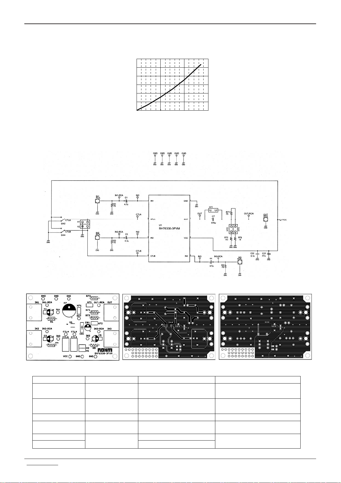
Fig.17 Result of Resistance Inserted to Improve BH76332FVM/BH76333FVM Frequency Response
www.rohm.com
© 2009 ROHM Co., Ltd. All rights reserved.
9/32
2009.04 - Rev.A
Page 10
BH76330FVM, BH76331FVM, BH76360FV, BH76361FV,
BH76332FVM, BH76333FVM, BH76362FV, BH76363FV
Technical Note
12. With clamp input type models (BH76330FVM and BH76332FVM), if the termination impedance of the video input pin
becomes higher, sync contractions or oscillation-related problems may occur. Evaluate temperature and other
characteristics carefully and use at 1 k
Fig. 18. Relation between Input Pin Termination Impedance and Amount of Sync Contraction
or less.
6
5
4
3
2
at input pin [%]
1
Amount of sync contraction
入力端子でのsync縮み量[%]
0
01k2k3k
入力終端抵抗Rin[Ω]
Input termination resistance Rin [Ω]
● Evaluation board pattern diagram and circuit diagram
Fig. 19. Evaluation Board Circuit Diagram
Parts list
Symbol Function Recommended value
R1 R3 R5 Input terminating resistor 75
C1 C3 C5
R71 Output resistor 75
C7
C01
C02
Input coupling
capacitor
Output coupling
capacitor
Decoupling capacitor
Fig. 20. Evaluation Board Pattern Diagram
See pages 6/16 to 7/16 to determine
See pages 6/16 to 7/16 to determine
10 µF
0.1 µF
Comments
-
B characteristics recommended
-
B characteristics recommended
B characteristics recommended
www.rohm.com
© 2009 ROHM Co., Ltd. All rights reserved.
10/32
2009.04 - Rev.A
Page 11

BH76330FVM, BH76331FVM, BH76360FV, BH76361FV,
p
BH76332FVM, BH76333FVM, BH76362FV, BH76363FV
Technical Note
● Reference data (1) BH76330FVM/BH76331FVM [unless otherwise specified, output capacitance C: 470 µF, RL = 150
20
BH76330FV
Ta =2 5 ℃
20
BH76330FV
VCC=5V
20
BH76331FV
Ta =2 5 ℃
BH76331FV
20
VCC=5V
15
15
15
15
10
回路電流[mA]
5
Circuit current [mA]
0
23456
Fig. 21 ICC1 vs. Supply Voltage Fig. 22 ICC1 vs. Ambient Temperature
Output capacitance C: 470 µF
出力C容量:470uF
出力Cレス
No out
ut capacitance
Supply Voltage [V]
電源電圧[V]
10
回路電流[mA]
5
Circuit current [mA]
0
-50 0 50 100
周囲温度[℃]
10
回路電流[mA]
5
Circuit current [mA]
0
23456
Supply Voltage [V]Ambient Temperature [℃] Ambient Temperature [℃]
電源電圧[V]
10
回路電流[mA]
5
Circuit current [mA]
0
-50 0 50 100
周囲温度[℃]
Fig. 23 ICC1 vs. Supply Voltage Fig.24 ICC1 vs. Ambient Temperature
BH76330/31FV
2.0
1.5
1.0
0.5
0.0
回路電流(STBY)[μA]
Circuit current (STBY) [μA]
-0.5
23456
Supply Voltage [V]
Fig.25 ICC2 vs. Supply Voltage
電源電圧[V]
Ta =2 5 ℃
BH76330/31FV
2.0
1.5
1.0
0.5
0.0
回路電流(STBY)[μA]
Circuit current (STBY) [μA]
-0.5
-50 0 50 100
Ambient Temperature [℃]
周囲温度[℃]
Fig.26 ICC2 vs. Ambient Temperature
VCC=5V
BH76330FV
6.0
5.0
4.0
3.0
最大出力レベル[Vpp]
Maximum output level [ Vpp]
2.0
23456
Supply Voltage [V]
電源電圧[V]
Ta =2 5 ℃
Fig.27 Vom vs. Supply Voltage
BH76360FV
3.0
2.8
2.6
2.4
2.2
最大出力レベル[Vpp]
Maximum output level [ Vpp]
2.0
-50 0 50 100
Ambient Temperature [℃]
周囲温度[℃]
VCC=3V
Fig.28 Vom vs. Ambient Temperature
BH76331FV
6.0
5.0
4.0
3.0
最大出力レベル[Vpp]
Maximum output level [ Vpp]
2.0
23456
Supply Voltage [V]
電源電圧[V]
Fig.29 Vom vs. Supply Voltage
Ta =2 5 ℃
BH76331FV
3.0
2.8
2.6
2.4
2.2
最大出力レベル[Vpp]
Maximum output level [ Vpp]
2.0
-50 0 50 100
Ambient Temperature [℃]
Fig.30 Vom vs. Ambient Temperature
周囲温度[℃]
VCC=3V
BH76330FV
6.3
6.2
6.1
6.0
5.9
電圧利得[dB]
Voltage gain [dB]
5.8
5.7
23 456
Supply Voltage [V] Ambient Temperature [℃]
Fig.31 G
電源電圧[V]
vs. Supply Voltage
V
Ta =2 5 ℃
BH76330FV
6.3
6.2
6.1
6.0
5.9
電圧利得[dB]
Voltage gain [dB]
5.8
5.7
-50 0 50 100
Fig.32 G
周囲温度[℃]
vs. Ambient Temperature
V
VCC=5V
BH76331FV
6.3
6.2
6.1
6.0
5.9
電圧利得[dB]
Voltage gain [dB]
5.8
5.7
23 456
Fig.33 G
Supply Voltage [V]
電源電圧[V]
vs. Supply Voltage Fig.34 GV vs. Ambient Temperature
V
Ta =2 5 ℃
BH76331FV
6.3
6.2
6.1
6.0
5.9
電圧利得[dB]
Voltage gain [dB]
5.8
5.7
-50 0 50 100
周囲温度[℃]
Ambient Temperature [℃]
VCC=5V
BH76330FV
1.0
0.5
0.0
-0.5
-1.0
-1.5
周波数特性(100k/10MHz)[dB]
-2.0
23456
Frequency response (100 kHz/10 MHz) [dB]
Fig.35 G
Supply Voltage [V]
電源電圧[V]
vs. Supply Voltage Fig.36 GF vs. Ambient Temperature
F
Ta =2 5 ℃
BH76330FV
1.0
0.5
0.0
-0.5
-1.0
-1.5
周波数特性(100k/10MHz)[dB]
-2.0
-50 0 50 100
Frequency response (100 kHz/10 MHz) [dB]
Ambient Temperature [℃]
周囲温度[℃]
VCC=5V
www.rohm.com
© 2009 ROHM Co., Ltd. All rights reserved.
11/3 2
2009.04 - Rev.A
Page 12

BH76330FVM, BH76331FVM, BH76360FV, BH76361FV,
]
]
p
p
BH76332FVM, BH76333FVM, BH76362FV, BH76363FV
BH76331FV
1.0
0.5
0.0
-0.5
-1.0
-1.5
周波数特性(100k/10MHz)[dB]
-2.0
23456
Frequency response (100 kHz/10 MHz) [dB]
Fig.37 G
Supply Voltage [V]
電源電圧[V]
vs. Supply Voltage
F
Ta =2 5 ℃
BH76331FV
1.0
0.5
0.0
-0.5
-1.0
-1.5
周波数特性(100k/10MHz)[dB]
-2.0
-50 0 50 100
Frequency response (100 kHz/10 MHz) [dB]
Fig.38 G
Ambient Temperature [℃]
周囲温度[℃]
vs. Ambient Temperature
F
VCC=5V
BH76330FV
5
0
-5
Gain[dB
-10
-15
1M 10M 100M
VCC=5V, Ta=25℃
Frequency[Hz]
Fig. 39 Frequency Response
BH76330/31FV
-65
-67
-69
-71
-73
-75
チャンネル間クロストーク(wors t)[d B]
23456
Crosstalk between channels (worst) [dB]
Fig.41 CT(worst) vs. Supply Voltage Fig.42 CT(worst) vs. Ambient Temperature Fig.43 MT(worst) vs. Supply Voltage
Supply Voltage [V]
電源電圧[V]
Ta =2 5 ℃
BH76330/31FV
-65
-67
-69
-71
-73
-75
チャンネル間クロストーク(worst)[dB]
Crosstalk between channels (worst) [dB]
-50 0 50 100
Ambient Temperature [℃]
周囲温度[℃]
VCC=5V
BH76330/31FV
-70
-72
-74
-76
-78
ミュート減衰量(wor st )[dB]
Mute attenuation (worst) [dB]
-80
23456
Supply Voltage [V]
電源電圧[V]
Ta =2 5 ℃
BH76330/31FV
20
15
CTL_A:0[V]
10
回路電流[mA]
5
Circuit current [mA]
0
0 0.5 1 1.5 2
Fig. 45 CTLb pin voltage vs Circuit Current
CTL_B pin voltage [V]
(CLT threshold )
VCC=5V, Ta=25℃
CTL_D端子電圧
BH76330/31FV
70
60
50
40
30
20
CTL端子流入電流[uA]
10
CTL pin influx current [µA]
0
-50 0 50 100
Fig.46 I
(Voltage applied to CTL pin = 2V)
周囲温度[℃]
Ambient Temperature [℃]
vs. Ambient Temperature
THH
VCC=5V
BH76330FV
2.0
1.5
1.0
微分利得[%]
0.5
Differential gain [%]
0.0
23 456
電源電圧[V]
Supply Voltage [V]
Ta =2 5 ℃
Fig.47 DG vs. Supply Voltage
BH76331FV
2.0
1.5
Ta =2 5 ℃
BH76331FV
2.0
1.5
VCC=5V
2.0
1.5
BH76330FV
出力C容量:470uF
Output capacitance C: 470 µF
No out
ut capacitance
出力Cレス
Ta =2 5 ℃
1.0
微分利得[%]
0.5
Differential gain [%]
0.0
23 456
Supply Voltage [V] Ambient Temperature [℃]
Fig.49 DG vs. Supply Voltage
電源電圧[V]
1.0
微分利得[%]
0.5
Differential gain [%]
0.0
-50 0 50 100
電源電圧[V]
Fig.50 DG vs. Ambient Temperature
1.0
微分位相[deg.]
0.5
Differential phase [deg.]
0.0
23456
Supply Voltage [V]
電源電圧[V]
Fig.51 DP vs. Supply Voltage
Technical Note
BH76331FV
5
0
-5
Gain[dB
-10
-15
1M 10M 100M
Fig. 40 Frequency Response
BH76330/31FV
-70
-72
-74
-76
-78
ミュート減衰量(worst)[dB]
Mute attenuation (worst) [dB]
-80
-50 0 50 100
Fig.44 MT(wrost) vs. Ambient Temperature
BH76330FV
2.0
1.5
1.0
微分利得[%]
0.5
Differential gain [%]
0.0
-50 0 50 100
Fig.48 DG vs. Ambient Temperature
BH76330FV
2.0
1.5
1.0
微分位相[deg.]
0.5
Differential phase [deg.]
0.0
-50 0 50 100
Ambient Temperature [℃]
Fig.52 DP vs. Ambient Temperature
VCC=5V, Ta=25℃
Frequency[Hz]
VCC=5V
周囲温度[℃]
Ambient Temperature [℃]
VCC=5V
電源電圧[V]
Ambient Temperature [℃]
VCC=5V
出力C容量:470uF
Output capacitance C: 470 µF
No out
ut capacitance
出力Cレス
電源電圧[V]
www.rohm.com
© 2009 ROHM Co., Ltd. All rights reserved.
12/32
2009.04 - Rev.A
Page 13

BH76330FVM, BH76331FVM, BH76360FV, BH76361FV,
BH76332FVM, BH76333FVM, BH76362FV, BH76363FV
Technical Note
BH76331FV
2.0
Ta =2 5 ℃
1.5
1.0
微分位相[deg.]
0.5
Differential phase [deg.]
0.0
23456
Fig.53 DP vs. Supply Voltage
電源電圧[V]
Supply Voltage [V]
BH76331FV
2.0
1.5
1.0
微分位相[deg.]
0.5
Differential phase [deg.]
0.0
-50 0 50 100
Ambient Temperature [℃]
電源電圧[V]
Fig.54 DP vs. Ambient Temperature
VCC=5V
BH76330/31FV
80
78
76
74
Y系S/N[dB]
Y S/N [dB]
72
70
23 456
Supply Voltage [V]
電源電圧[V]
Fig.55 SN
vs. Supply Voltage
Y
Ta =2 5 ℃
BH76330/31FV
80
78
76
74
Y系S/N[dB]
Y S/N [dB]
72
70
-50 0 50 100
Ambient Temperature [℃]
周囲温度[℃]
Fig.56 SN
vs. Ambient Temperature
Y
VCC=5V
BH76330/31FV
80
78
76
74
C系S/N(AM )[dB]
C S/N (AM) [dB]
72
70
23456
Supply Voltage [V]
Fig.57 SN
電源電圧[V]
vs. Supply Voltage
CA
Ta =2 5 ℃
BH76330/31FV
80
78
76
74
C系S /N(AM )[dB]
C S/N (AM) [dB]
72
70
-50 0 50 100
Ambient Temperature [℃]
周囲温度[℃]
Fig.58 SN
vs. Ambient Temperature
CA
VCC=5V
BH76330/31FV
70
69
68
67
C S/N (PM) [dB]
C系S/N(PM)[dB]
66
65
23456
Supply Voltage [V]
電源電圧[V]
Fig.59 SN
vs. Supply Voltage
CP
Ta =2 5 ℃
BH76330/31FV
70
69
68
67
C系S /N(PM )[dB]
C S/N (PM) [dB]
66
65
-50 0 50 100
Fig.60 SN
周囲温度[℃]
Ambient Temperature [℃]
vs. Ambient Temperature
CP
VCC=5V
● Reference data (2) BH76332FVM/BH76333FVM [unless otherwise specified, output capacitance C: 470 µF, RL = 10 k]
BH76332FV
20
Ta =2 5 ℃
BH76332FV
20
VCC=5V
BH76333FV
20
Ta =2 5 ℃
BH76333FV
20
VCC=5V
15
15
15
15
10
10
10
10
回路電流[mA]
5
Circuit current [mA]
0
23456
Supply Voltage [V]
Fig.61 ICC1 vs. Supply Voltage Fig.62 ICC1 vs. Ambient Temperature
電源電圧[V]
回路電流[mA]
5
Circuit current [mA]
0
-50 0 50 100
Ambient Temperature [℃]
周囲温度[℃]
回路電流[mA]
5
Circuit current [mA]
0
23456
Supply Voltage [V]
Fig.63 ICC1 vs. Supply Voltage Fig.64 ICC1 vs. Ambient Temperature
電源電圧[V]
回路電流[mA]
5
Circuit current [mA]
0
-50 0 50 100
周囲温度[℃]
Ambient Temperature [℃]
BH76332/33FV
2.0
1.5
1.0
0.5
0.0
回路電流(STBY)[μA]
Circuit current (STBY) [μA]
-0.5
23456
Supply Voltage [V]
電源電圧[V]
Fig.65 ICC2 vs. Supply Voltage
Ta =2 5 ℃
BH76332/33FV
2.0
1.5
1.0
0.5
0.0
回路電流(STBY)[μA]
Circuit current (STBY) [μA]
-0.5
-50 0 50 100
Ambient Temperature [℃] Supply Voltage [V]
周囲温度[℃]
Fig.66 ICC2 vs. Ambient Temperature
VCC=5V
BH76332FV
5.0
4.0
3.0
2.0
最大出力レベル[Vpp]
Maximum output level [ Vpp]
1.0
23456
電源電圧[V]
Fig.67 Vom vs. Supply Voltage
Ta =2 5 ℃
BH76332FV
2.5
2.3
2.1
1.9
1.7
最大出力レベル[Vpp]
Maximum output level [ Vpp]
1.5
-50 0 50 100
Ambient Temperature [℃]
Fig.68 Vom vs. Ambient Temperature
周囲温度[℃]
VCC=3V
www.rohm.com
© 2009 ROHM Co., Ltd. All rights reserved.
13/32
2009.04 - Rev.A
Page 14

BH76330FVM, BH76331FVM, BH76360FV, BH76361FV,
BH76332FVM, BH76333FVM, BH76362FV, BH76363FV
BH76333FV
5.0
Ta =2 5 ℃
4.0
3.0
2.0
最大出力レベル[Vpp]
Maximum output level [ Vpp]
1.0
23456
Supply Voltage [V]
電源電圧[V]
Fig.69 Vom vs. Supply Voltage
BH76333FV
2.5
2.3
2.1
1.9
1.7
最大出力レベル[Vpp]
Maximum output level [ Vpp]
1.5
-50 0 50 100
Ambient Temperature [℃]
VCC=3V
周囲温度[℃]
Fig.70 Vom vs. Ambient Temperature
BH76332FV
0.4
0.2
0.0
-0.2
電圧利得[dB]
Voltage gain [dB]
-0.4
-0.6
23456
Supply Voltage [V]
電源電圧[V]
Fig.71 G
vs. Supply Voltage
V
Ta =2 5 ℃
BH76333FV
0.4
0.2
0.0
-0.2
電圧利得[dB]
Voltage gain [dB]
-0.4
-0.6
23456
Supply Voltage [V]
電源電圧[V]
Fig.73 GV vs. Supply Voltage Fig.74 GV vs. Ambient Temperature
Ta =2 5 ℃
BH76333FV
0.4
0.2
0.0
-0.2
電圧利得[dB]
Voltage gain [dB]
-0.4
-0.6
-50 0 50 100
Ambient Temperature [℃]
周囲温度[℃]
VCC=5V
BH76332FV
1.0
0.5
0.0
-0.5
-1.0
-1.5
周波数特性(100k/30MHz)[dB]
-2.0
23456
Frequency response (100 kHz/10 MHz) [dB]
Supply Voltage [V]
Fig.75 G
電源電圧[V]
vs. Supply Voltage Fig.76 GF vs. Ambient Temperature
F
Ta =2 5 ℃
BH76333FV
1.0
0.5
0.0
-0.5
-1.0
-1.5
周波数特性(100k/30MHz)[dB]
-2.0
23456
Frequency response (100 kHz/10 MHz) [dB]
Fig.77 G
Supply Voltage [V]
電源電圧[V]
vs. Supply Voltage Fig.78 GF vs. Ambient Temperature Fig. 79 Frequency Response Fig. 80 Frequency Response
F
Ta =2 5 ℃
BH76333FV
1.0
0.5
0.0
-0.5
-1.0
-1.5
周波数特性(100k/30MHz)[dB]
-2.0
-50 0 50 100
Frequency response (100 kHz/10 MHz) [dB]
Ambient Temperature [℃]
VCC=5V
周囲温度[℃]
BH76332FV
2
1
0
-1
-2
Gain[dB]
-3
-4
-5
1M 10M 100M
VCC=5V ,Ta=25℃
Frequency[Hz]
BH76332/33FV
-65
-67
-69
-71
-73
-75
チャンネル間クロストーク(wors t)[d B]
23456
Crosstalk between channels (worst) [dB]
Fig.81 CT(worst) vs. Supply Voltage Fig.82 CT(worst) vs. Ambient Temperature Fig.83 MT(worst) vs. Supply Voltage
電源電圧[V]
Supply Voltage [V]
Ta =2 5 ℃
BH76332/33FV
-65
-67
-69
-71
-73
-75
チャンネル間クロストーク(worst)[dB]
-50 0 50 100
Crosstalk between channels (worst) [dB]
Ambient Temperature [℃]
周囲温度[℃]
VCC=5V
BH76332/33FV
-70
-72
-74
-76
-78
Mute attenuation (worst) [dB]
ミュート減衰量(worst)[dB]
-80
23456
Supply Voltage [V]
電源電圧[V]
Ta =2 5 ℃
Technical Note
BH76332FV
0.4
0.2
0.0
-0.2
電圧利得[dB]
Voltage gain [dB]
-0.4
-0.6
-50 0 50 100
Ambient Temperature [℃]
周囲温度[℃]
Fig.72 G
vs. Ambient Temperature
V
BH76332FV
1.0
0.5
0.0
-0.5
-1.0
-1.5
周波数特性(100k/30MHz)[dB]
-2.0
-50 0 50 100
Frequency response (100 kHz/10 MHz) [dB]
Ambient Temperature [℃]
周囲温度[℃]
BH76333FV
2
1
0
-1
-2
Gain [d B]
-3
-4
-5
1M 10M 100M
Frequency[Hz]
BH76332/33FV
-70
-72
-74
-76
-78
ミュート減衰量(worst)[dB]
Mute attenuation (worst) [dB]
-80
-50 0 50 100
Ambient Temperature [℃]
Fig.84 MT(wrost) vs. Ambient Temperature
VCC=5V
VCC=5V
VCC=5V ,Ta=25℃
VCC=5V
周囲温度[℃]
www.rohm.com
© 2009 ROHM Co., Ltd. All rights reserved.
14/32
2009.04 - Rev.A
Page 15

BH76330FVM, BH76331FVM, BH76360FV, BH76361FV,
BH76332FVM, BH76333FVM, BH76362FV, BH76363FV
BH76332/33FV
20
15
CTL_A:0[V]
10
5
回路電流[mA]
Circuit current [mA]
0
0 0.5 1 1.5 2
Fig.85 CTLb pin voltage vs Circuit Current
CTL_B pin voltage [V]
(CLT threshold )
VCC=5V, Ta=25℃
CTL_D端子電圧
BH76332/33FV
70
60
50
40
30
20
CTL端子流入電流[uA]
10
CTL pin influx current [µA]
0
-50 0 50 100
Fig.86 I
(Voltage applied to CTL pin = 2V)
周囲温度[℃]
Ambient Temperature [℃]
vs. Ambient Temperature
THH
2.0
BH76333FV
Ta =2 5 ℃
BH76333FV
2.0
1.5
1.5
1.0
微分利得[%]
0.5
Differential gain [%]
1.0
微分利得[%]
0.5
Differential gain [%]
0.0
23 456
Fig.89 DG vs. Supply Voltage
電源電圧[V]
Supply Voltage [V]
0.0
-50 0 50 100
Fig.90 DG vs. Ambient Temperature Fig.91 DP vs. Supply Voltage
電源電圧[V]
Ambient Temperature [℃]
BH76333FV
2.0
1.5
1.0
微分位相[deg.]
0.5
Differential phase [deg.]
0.0
23456
Supply Voltage [V]
電源電圧[V]
Fig.93 DP vs. Supply Voltage
Ta =2 5 ℃
BH76333FV
2.0
1.5
1.0
微分位相[deg.]
0.5
Differential phase [deg.]
0.0
-50 0 50 100
Fig.94 DP vs. Ambient Temperature
電源電圧[V]
Ambient Temperature [℃]
BH76332/33FV
80
78
Ta =2 5 ℃
BH76332/33FV
80
78
76
74
C S/N (AM) [dB]
C系S/N(AM )[dB]
72
70
23456
Supply Voltage [V]
Fig.97 SN
電源電圧[V]
vs. Supply Voltage
CA
76
74
C S/N (AM) [dB]
C系S /N(AM )[dB]
72
70
-50 0 50 100
Ambient Temperature [℃]
Fig.98 SN
周囲温度[℃]
vs. Ambient Temperature
CA
VCC=5V
VCC=5V
VCC=5V
VCC=5V
BH76332FV
2.0
1.5
1.0
微分利得[%]
0.5
Differential gain [%]
0.0
23 456
Supply Voltage [V]
電源電圧[V]
Fig.87 DG vs. Supply Voltage
BH76332FV
2.0
1.5
1.0
微分位相[deg.]
0.5
Differential phase [deg.]
0.0
23456
BH76332/33FV
80
78
76
74
Y S/N [dB]
Y系S/N[dB]
72
70
23456
Fig.95 SN
BH76332/33FV
70
69
68
67
C S/N (PM) [dB]
C系S/N(PM)[dB]
66
65
23456
Fig.99 SN
電源電圧[V]
Supply Voltage [V]
Ta =2 5 ℃
Supply Voltage [V]
電源電圧[V]
vs. Supply Voltage
Y
Supply Voltage [V]
電源電圧[V]
vs. Supply Voltage
CP
Ta =2 5 ℃
Ta =2 5 ℃
Ta =2 5 ℃
Technical Note
BH76332FV
2.0
1.5
1.0
微分利得[%]
Differential gain [%]
0.5
0.0
-50 0 50 100
Ambient Temperature [℃]
Fig.88 DG vs. Ambient Temperature
2.0
1.5
1.0
微分位相[deg.]
0.5
Differential phase [deg.]
0.0
-50 0 50 100
Fig.92 DP vs. Ambient Temperature
80
78
76
74
Y S/N [dB]
Y系S/N[dB]
72
70
-50 0 50 100
Fig.96 SN
70
69
68
67
C S/N (PM) [dB]
C系S /N(PM )[dB]
66
65
-50 0 50 100
Fig.100 SN
電源電圧[V]
BH76332FV
電源電圧[V]
Ambient Temperature [℃]
BH76332/33FV
周囲温度[℃]
Ambient Temperature [℃]
vs. Ambient Temperature
Y
BH76332/33FV
周囲温度[℃]
Ambient Temperature [℃]
vs. Ambient Temperature
CP
VCC=5V
VCC=5V
VCC=5V
VCC=5V
www.rohm.com
© 2009 ROHM Co., Ltd. All rights reserved.
15/32
2009.04 - Rev.A
Page 16

BH76330FVM, BH76331FVM, BH76360FV, BH76361FV,
BH76332FVM, BH76333FVM, BH76362FV, BH76363FV
Technical Note
● External dimensions and label codes
Max 3.25 (include . BURR)
7
6 3
3 0
Lot. No.
Model Code
BH76330FV 76330
BH76331FV 76331
BH76332FV 76332
BH76333FV 76333
MSOP8 (unit: mm )
Fig. 101 External Dimensions of BH7633xFVM Series Package
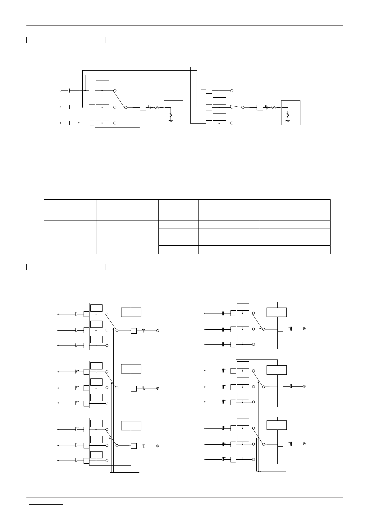
● When used with 6-input, 1-output video switch BH7636xFV
Fig. 14 above shows an application example in which two of these ICs are used. When the similar IC models BH7636xFV
and BH7633xFVM are used at the same time, the type of configuration shown below can be combined. In such cases,
input coupling capacitors can be used, as in the application example in Fig. 14.
External input
外部入力
Navigation
ナビ画面
screen
Rear camera
リアカメラ
TV
DVD
※3
※1
IIN1
IIN2
IIN3
IIN4
IIN5
IIN6
2
4
6
8
9
11
Clamp
Clamp
Clamp
Clamp
Clamp
Clamp
BH76360FV
16
OUT
※2
75Ω
Front
フロントモニタ
monitor
75Ω
1
*
Input coupling capacitor can be used with
this.
2
*
Output coupling capacitors can be omitted
when using BH76330FVM or BH76360FV,
and this helps reduce the number of parts.
3
*
Any inputs that are not used should be
connected directly to VCC or shorted with
GND via a capacitor.
IIN1
IIN2
IIN3
Clamp
1
Clamp
3
Clamp
5
BH76330FVM
16
OUT
※2
75Ω
Rear
リアモニタ
monitor
75Ω
Fig. 102 Application Example in which BH76330FVM and BH76360FV Are Used Concurrently
For details of BH7636xFV, see the BH7636xFV Series Application Notes.
www.rohm.com
© 2009 ROHM Co., Ltd. All rights reserved.
16/32
2009.04 - Rev.A
Page 17

BH76330FVM, BH76331FVM, BH76360FV, BH76361FV,
BH76332FVM, BH76333FVM, BH76362FV, BH76363FV
Technical Note
Line-up of products with built-in video amplifier and video driver
6-input, 1-output video switch
BH76360FV, BH76361FV, BH76362FV, BH76363FV
●General
BH76360FV, BH76361FV, BH76362FV, and BH76363FV are video signal switching ICs, each with six inputs and one circuit
input, which feature wide dynamic range and frequency response. Since these ICs can be used with low voltage starting at
VCC = 2.8 V, they are applicable not only in stationary devices but also in mobile devices.
This product line-up supports a broad range of input signals, depending on whether or not a 6-dB video amplifier and video
driver are included and what combination of sync tip clamp type and bias (resistor termination) type inputs are used.
●Features
1) Able to use a wide range of power supply voltage, from 2.8 V to 5.5 V
2) Wide output dynamic range
3) Excellent frequency response
(BH76360FV, BH76361FV:100kHz/10MHz 0dB[Typ.]、BH76362FV, BH76363FV:100kHz/30MHz 0dB[Typ.])
4) No crosstalk between channels (Typ.-65dB, f=4.43MHz)
5) Built-in mute function (Typ.-65dB, f=4.43MHz)
6) Built-in standby function, circuit current during standby is 0 µA (Typ.)
7) Sync tip clamp input (BH76360FV, BH76362FV)
8) Bias input (Zin=150kΩ) (BH76361FV, BH76363FV)
9) 6-dB amp and 75 driver are built in (BH76360FV, BH76361FV)
10) Enables two load drivers [when using output coupling capacitor](BH76360FV, BH76361FV)
11) Able to be used without output coupling capacitor (BH76360FV)
12) SSOP-B16 compact package
●Applications
Input switching in car navigation systems, TVs, DVD systems, etc.
●Line-up
BH76360FV BH76361FV BH76362FV BH76363FV
Supply voltage 2.8 V to 5.5 V
Amp gain 6dB -0.1dB
Video driver Included -
Frequency response 100kHz/10MHz 0dB (Typ.) 100kHz/30MHz 0dB (Typ.)
Input type
●Absolute maximum ratings (Ta = 25℃)
Parameter Symbol Limits Unit
Supply voltage VCC 7.0 V
Power dissipation Pd 450 *1 mW
Input voltage range VIN 0 to VCC+0.2 V
Operating temperature
range
Storage temperature
range
●Operation range (Ta = 25℃)
Parameter Symbol Min. Typ. Max Unit
Supply voltage VCC 2.8 5.0 5.5 V
Sync tip
clamp
*1 When used while Ta = 25℃, 4.7 mW is dissipated per 1℃
Mounted on 70 mm x 70 mm x 1.6 mm glass epoxy board
Bias
(Zin = 150 k)
Topr
Ts tg
Sync tip
clamp
-40 to +85 ℃
-55 to +125 ℃
(Zin = 150 k)
Bias
www.rohm.com
© 2009 ROHM Co., Ltd. All rights reserved.
17/32
2009.04 - Rev.A
Page 18

BH76330FVM, BH76331FVM, BH76360FV, BH76361FV,
BH76332FVM, BH76333FVM, BH76362FV, BH76363FV
Technical Note
●Electrical characteristics 1 (unless otherwise specified, Ta=25℃、VCC=5V)
Parameter Symbol
76360 76361 76362 76363
Typ.
Unit Conditions
Circuit current 1 ICC1 12 11 mA When no signal
Circuit current 2 ICC2 0.0 uA During standby
Circuit current 3
ICC3-1 13 12
ICC3-2 19 -
During output of color bar signal
mA
During output of color bar signal
(no C in output)
Maximum output level VOM 4.6 3.8 3.4 Vpp f=10kHz, THD=1%
Voltage gain GV 6.0 -0.1 dB Vin=1.0Vpp, f=100kHz
0 - dB Vin=1.0Vpp, f=10MHz/100kHz
G
Frequency response
Crosstalk between
channels
F1
GF2 - 0 dB Vin=1.0Vpp, f=30MHz/100kHz
C
-65 dB Vin=1.0Vpp, f=4.43MHz
T
Mute attenuation MT -65 dB Vin=1.0Vpp, f=4.43MHz
CTL pin switch level
CTL pin inflow current I
VTHH 1.2
VTHL 0.45
50
THH
V High Level threshold voltage
Min
V Low Level threshold voltage
Max
uA CTL pin = 2.0 V applied
Max
Input impedance Zin - 150 - 150 kΩ
Differential gain DG 0.3 %
-1 0.7 0.3
D
Differential phase
P
DP-2 0.0 - Same condition as above (no C in output)
Y-related S/N SNY +75 +78 dB
C-related S/N [AM] SNCA +75
C-related S/N [PM] SNCP +65
Vin=1.0Vpp
Standard stair step signal
deg.
Vin = 1.0 Vpp, bandwidth: 100 k to 6 MHz
100% white video signal
Vin = 1.0 Vpp, bandwidth: 100 to 500 kHz
dB
100% chroma voltage signal
●Electrical characteristics 2 (unless otherwise specified, Ta = 25℃, VCC = 3 V)
Parameter Symbol
76360 76361 76362 76363
Typ.
Unit Conditions
Circuit current 1 ICC1 10 mA When no signal
Circuit current 2 ICC2 0.0 uA During standby
ICC3-1 11 10 mA During output of color bar signal
Circuit current 3
ICC3-2 17 -
During output of color bar signal
(no C in output)
Maximum output level VOM 2.7 2.8 1.8 1.9 Vpp f=10kHz, THD=1%
Voltage gain GV 6.0 -0.1 dB Vin=1.0Vpp, f=100kHz
0 - dB Vin=1.0Vpp, f=10MHz/100kHz
G
Frequency response
Crosstalk between
channels
F1
GF2 - 0 dB Vin=1.0Vpp, f=30MHz/100kHz
C
-65 dB Vin=1.0Vpp, f=4.43MHz
T
Mute attenuation MT -65 dB Vin=1.0Vpp, f=4.43MHz
CTL pin switch level
CTL pin inflow current I
VTHH 1.2
VTHL 0.45
50
THH
V High Level threshold voltage
Min
V Low Level threshold voltage
Max
uA CTL pin = 2.0 V applied
Max
Input impedance Zin - 150 - 150 kΩ
Differential gain DG 0.3 %
Differential phase
DP-1 1.0 0.3
DP-2 0.5 - Same condition as above (no C in output)
Y-related S/N SNY +75 +78 dB
C-related S/N [AM] SNCA +75 dB
C-related S/N [PM] SNCP +65 dB
(Note) Re: ICC3, VOM, GV, GF, CT, MT, DG, DP, SNY, SNCA, SNCP parameters
BH76360FV, BH76361FV: RL = 150
BH76362FV, BH76363FV: RL = 10 k
Vin=1.0Vpp
Standard stair step signal
deg.
Vin = 1.0 Vpp, bandwidth: 100 k to 6 MHz
100% white video signal
Vin = 1.0 Vpp, bandwidth: 100 to 500 kHz
100% chroma video signal
www.rohm.com
© 2009 ROHM Co., Ltd. All rights reserved.
18/32
2009.04 - Rev.A
Page 19

BH76330FVM, BH76331FVM, BH76360FV, BH76361FV,
BH76332FVM, BH76333FVM, BH76362FV, BH76363FV
●Control pin settings
CTLA CTLB CTLC CTLD
IN1 L(OPEN) L(OPEN) L(OPEN) H
IN2 H L(OPEN) L(OPEN) H
IN3 L(OPEN) H L(OPEN) H
IN4 H H L(OPEN) H
IN5 L(OPEN) L(OPEN) H H
IN6 H L(OPEN) H H
MUTE * H H H
STBY * * * L(OPEN)
* L(OPEN) or H either is possible
●Block diagram
IN4 GND IN3 GND IN2 VCC IN1 PVCC
8 7 6 5 4 3 2 1
Sync_Tip
Clamp
Sync_Tip
Clamp
Sync_Tip
Clamp
Sync_Tip
Clamp
6dB 75Ω
Sync_Tip
Clamp
9 10 11 12 13 14 15 16
IN5
CTLA
logic
Sync_Tip
Clamp
CTLB CTLC PGND OUT
IN6
CTLD
Fig.1 BH76360FV
IN4 GND I N3 GND IN2 VC C IN1 PVCC
8 7 6 5 4 3 2 1
Sync_Tip
Clamp
Sync_Tip
Clamp
Sync_Tip
Clamp
Sync_Tip
Clamp
0dB
Sync_Tip
Clamp
9 10 11 12 13 14 15 16
IN5
CTLA
logic
Sync_Tip
Clamp
CTLB CTLC PGND OUT
IN6
CTLD
Fig.3 BH76362FV Fig.4 BH76363FV
IN4 GND I N3 GND IN2 VC C IN1 PVCC
87654 3 21
BIAS BIAS BIAS
BIAS BIAS
9 10 11 12 13 14 15 16
IN5
CTLA
BIAS
6dB 75Ω
logic
CTLB CTLC PGND OUT
IN6
CTLD
Fig.2 BH76361FV
IN4 GND I N3 GND IN2 VC C IN1 PVCC
87654 3 21
BIAS BIAS BIAS
BIAS BIAS
9 10 11 12 13 14 15 16
IN5
CTLA
BIAS
logic
CTLB CTLC PGND OUT
IN6
CTLD
Technical Note
0dB
www.rohm.com
© 2009 ROHM Co., Ltd. All rights reserved.
19/32
2009.04 - Rev.A
Page 20

BH76330FVM, BH76331FVM, BH76360FV, BH76361FV,
BH76332FVM, BH76333FVM, BH76362FV, BH76363FV
●I/O equivalent circuit diagrams
Input pins
Sync tip clamp input
BH76360FV / BH76362FV
PIN No. Name Equivalent circuit PIN No. Name Equivalent circuit
2
4
6
8
9
11
IN1
IN2
IN3
IN4
IN5
IN6
IN
100Ω
Bias input
BH76361FV / BH76363FV
2
4
6
8
9
11
IN1
IN2
IN3
IN4
IN5
IN6
IN
100Ω
Technical Note
150kΩ
Video signal input pin is used for sync tip clamp input.
・DC potential
BH76360FV:1.5V BH76362FV:1.0V
Control pins
PIN No. Name Equivalent circuit
10
12
13
14
Switches operation mode [active or standby] and input
pin.
Threshold level is 0.45 V to 1.2 V.
Output pin
With video driver
BH76360FV / BH76361FV
PIN No. Name Equivalent circuit PIN No. Name
CTLA
CTLB
CTLC
CTLD
CTL
50kΩ
200kΩ
200k
250kΩ
Video signal input pin is used for bias type input. Input
impedance is 150 k.
・DC potential
BH76361FV:3.1V BH76363FV:2.5V
Ω
Without video driver
BH76362FV / BH76363FV
OUT
16 OUT
14kΩ
Video signal output pin. Able to drive loads up to 75
(dual drive).
・DC potential
BH76360FV:0.16V BH76361FV:2.5V
Note 1) The above DC potential is only when VCC = 5 V. This value is a reference value and is not guaranteed.
Note 2) Numerical values shown in these figures are design values, and compliance to standards is not guaranteed.
www.rohm.com
© 2009 ROHM Co., Ltd. All rights reserved.
16 OUT
3.0mA
Video signal output pin.
・DC potential
BH76362FV:0.3V BH76363FV:1.8V
20/32
OUT
2009.04 - Rev.A
Page 21

BH76330FVM, BH76331FVM, BH76360FV, BH76361FV,
BH76332FVM, BH76333FVM, BH76362FV, BH76363FV
●Test Circuit Diagrams
VCC
VCC
0.01μF 10μF
A
0.01μF
50Ω
50Ω
50Ω
50Ω
0.01μF
0.01μF
0.01μF
PVCC
VCC
GND
GND
OUT
1
Clamp/
IN1
Bias
2
75Ω
3
Clamp/
IN2
Bias
4
5
Clamp/
IN3
Bias
6
6dB
logic
Clamp/
Bias
7
Clamp/
IN4
Bias
8
Clamp/
Bias
16
PGND
15
CTLD
14
CTLC
13
CTLB
12
IN6
11
CTLA
10
IN5
9
10μF
75Ω
V V75Ω
A
A
A
0.01μF
50Ω
A
0.01μF
50Ω
VCC
VCC
0.01μF10μF
A
50Ω
50Ω
50Ω
0.01μF
0.01μF
0.01μF
PVCC
VCC
GND
GND
1
Clamp/
IN1
Bias
2
3
Clamp/
IN2
Bias
4
0dB
5
Clamp/
IN3
Bias
6
7
Clamp/
IN4
0.01μF
50Ω
Bias
8
Fig.5 BH76360FV/BH76361FV Test Circuit Diagram
● Application circuit examples
VCC
VIDEO_IN
VIDEO_IN
VIDEO_IN
VIDEO_IN
VCC
VIDEO_IN
VIDEO_IN
VIDEO_IN
VIDEO_IN
Test circuit diagrams are used for shipment inspections, and differ from application circuits.
出力コンデンサレス
で使用する場合
0.1μF 10μF
PVCC
1
Sync_Tip
Clamp
IN1
2
0.1μF
0.1μF
0.1μF
0.1μF
0.1μF 10μF
0.1μF
0.1μF
0.1μF
0.1μF
VCC
3
Sync_Tip
IN2
Clamp
4
GND
5
Sync_Tip
IN3
Clamp
6
GND
7
Sync_Tip
Clamp
IN4
8
Fig.7 BH76360FV
PVCC
1
Sync_Tip
Clamp
IN1
2
VCC
3
Sync_Tip
IN2
Clamp
4
GND
5
Sync_Tip
IN3
Clamp
6
GND
7
Sync_Tip
Clamp
IN4
8
Fig.9 BH76362FV Fig.10 BH76363FV
0dB
6dB
75Ω
logic
Sync_Tip
Clamp
Sync_Tip
Clamp
logic
Sync_Tip
Clamp
Sync_Tip
Clamp
OUT
16
PGND
15
CTLD
14
CTLC
13
CTLB
12
IN6
11
CTLA
10
IN5
9
OUT
16
PGND
15
CTLD
14
CTLC
13
CTLB
12
IN6
11
CTLA
10
IN5
9
OUT
16
75Ω
VIDEO_OUT
470μF
75Ω
VIDEO_OUT
0.1μF
VIDEO_IN
0.1μF
VIDEO_IN
VIDEO_OUT
0.1μF
VIDEO_IN
0.1μF
VIDEO_IN
Fig.6 BH76362FV/BH76363FV Test Circuit Diagram
VCC
VIDEO_IN
VIDEO_IN
VIDEO_IN
VIDEO_IN
0.1μF10μF
4.7μF
4.7μF
4.7μF
4.7μF
PVCC
1
BIAS
IN1
2
VCC
3
BIAS
IN2
4
GND
5
BIAS
IN3
6
GND
7
BIAS BIAS
IN4
8
Fig.8 BH76361FV
VCC
VIDEO_IN
VIDEO_IN
VIDEO_IN
VIDEO_IN
0.1μF10μF
4.7μF
4.7μF
4.7μF
4.7μF
PVCC
1
BIAS
IN1
2
VCC
3
BIAS
IN2
4
GND
5
BIAS
IN3
6
GND
7
BIAS BIAS
IN4
8
0dB
See pages 6/16 to 10/16 for description of how to determine the capacity of I/O coupling capacitors.
75Ω
6dB
Technical Note
OUT
16
10μF
10kΩ
PGND
15
CTLD
A
14
CTLC
A
13
CTLB
OUT
16
PGND
15
CTLD
14
CTLC
13
CTLB
12
IN6
11
CTLA
10
IN5
9
OUT
16
PGND
15
CTLD
14
CTLC
13
CTLB
12
IN6
11
CTLA
10
IN5
9
12
IN6
11
CTLA
10
IN5
9
A
0.01μF
50Ω
A
0.01μF
50Ω
470μF
75Ω
4.7μF
4.7μF
VIDEO_OUT
4.7μF
4.7μF
logic
Clamp/
Clamp/
logic
logic
Bias
Bias
BIAS
BIAS
V V
VIDEO_OUT
VIDEO_IN
VIDEO_IN
VIDEO_IN
VIDEO_IN
www.rohm.com
© 2009 ROHM Co., Ltd. All rights reserved.
21/32
2009.04 - Rev.A
Page 22

BH76330FVM, BH76331FVM, BH76360FV, BH76361FV,
BH76332FVM, BH76333FVM, BH76362FV, BH76363FV
Technical Note
●Cautions for selection and use of application parts
When using this IC by itself ①
Input type
Method for determining capacity of input coupling capacitor
Sync_Tip_Clamp 10MΩ 0.1uF
Bias 150kΩ 4.7uF
Input impedance
Zin
The HPF is comprised of an input coupling capacitor and the internal input impedance Zin of the IC. Since the fc value of this HPF is
determined using the following equation (a), the above recommended capacity for the input capacitor is derived. Usually, the cutoff
frequency fc is several Hz.
fc = 1 / (2π × C × Zin)・・・・(a)
When evaluating the sag characteristics and determining the capacity of the capacitor during video signal input, a horizontal stripe signal
called "H bar" (shown in Fig. 10) is suitable, and this type of signal is used instead of a color bar signal to evaluate characteristics and
determine capacity.
Capacity of input coupling
capacitor (recommended value)
Capacity of output coupling
capacitor (recommended value)
470uF~1000uF
Method for determining capacity of output coupling capacitor
The output pins of models with a 75 driver [BH76360FV and BH76361FV] have an HPF comprised of an output coupling capacitor and
load resistance R
approximately 470 µF to 1000 µF.
As for models without the 75 driver, an HPF is similarly comprised using the capacity of the output coupling capacitor and the input
impedance of the IC connected at the next stage, and the capacitance required for the output coupling capacitor should be estimated using
equation (a).
Fig.11 Example of Screen with Obvious Sag (H-bar Signal)
(= 150). When fc is set to approximately 1 Hz or 2 Hz, the capacity of the output coupling capacitor needs to be
L
When this IC is used as a standalone device ②
In models that include a 75 driver [BH76360FV and BH76361FV], up to two monitors (loads) can be connected (a connection example is
shown in Fig. 12). When there are multiple loads, the number of output coupling capacitors must be increased or a larger capacitance must
monitor
monitor
75Ω
75Ω
OUT
(470×2)μF
16
75Ω
75Ω
monitor
75Ω
monitor
75Ω
be used, based on the table shown below.
470μF
OUT
16
470μF
75Ω
75Ω
Fig. 12 (a) Application Circuit Example 1 (Two Drives)
Fig. 12 (b) Application Circuit Example 2 (Two Drives)
Application circuit example No. of output capacitors Capacitance per output capacitor (recommended values)
Fig12(a) No. of drives required 470 µF to 1000 µF (same as with one drive)
Fig12(b) 1 (No. of drive × 470 µF to 1000) uF
When this IC is used as a standalone device ③
The BH76360FV is the only model that can be used without an output coupling capacitor.
This use method not only enables reductions in board space and part-related costs, but it is able to improve the sag characteristics by
improving low-range frequency response. However, when the output coupling capacitor is omitted, a direct current flows to the connected
set, so the specifications of the connected set should be noted carefully before starting use.
Note also that only one load can be connected when the output coupling capacitor is omitted.
monitor
75Ω
75Ω
BH76360FV
OUT
16
Voltage at output ≒0.16V
When this voltage load resistance is applied,
a direct current is generated.
www.rohm.com
© 2009 ROHM Co., Ltd. All rights reserved.
Fig.13 Application Example without Output Coupling Capacitor
22/32
2009.04 - Rev.A
Page 23

BH76330FVM, BH76331FVM, BH76360FV, BH76361FV,
BH76332FVM, BH76333FVM, BH76362FV, BH76363FV
When using several of these ICs ①
When several of these ICs are used, it enables applications in which separate images are output to the car navigation system's front and
rear monitors.
Technical Note
VIDEO IN
VIDEO IN
VIDEO IN
IN1
2
IN2
4
IN3
6
Clamp
/Bias
Clamp
/Bias
Clamp
/Bias
Clamp
/Bias
IN1
2
16
OUT
470μF
Front monitor Rear monitor
75Ω
75Ω
IN2
IN3
4
6
Clamp
/Bias
Clamp
/Bias
Fig.14 Application Example when Using Several ICs
16
OUT
470μF
75Ω
75Ω
When several ICs are used at the same time, the number of parallel connections of input impedance equals the number of ICs being used,
which reduces the input impedance. This also raises the fc value of the HPF formed at the input pin block, so the capacitance of the input
coupling capacitor must be increased according to equation (a). The recommended values for calculation results are listed in the table
below.
When a clamp is used as the input type, the original input impedance becomes much greater, and if two or three are used at the same
time there is no need to change the capacitance of the input coupling capacitor.
Capacitance of input
coupling capacitor
(recommended values)
Input type Input impedance per IC
Sync_Tip_Clamp Approx. 10 M
Bias 150kΩ
Number of ICs
used
Tota l
input impedance
2 Approx. 5 M 0.1uF
3 Approx. 3 M 0.1uF
2 75kΩ 6.8uF~
3 50kΩ 10uF~
When using several of these ICs ②
When three bias input type models (BH76361FV or BH76363FV) are used in parallel, they can be used for RGB signal switching
applications. Likewise, when one clamp input type model (BH76360FV or BH76362FV) is connected in parallel with two bias input type
models (a total of three ICs used in parallel), they can be used for component signal switching applications. The same method can be used
to determine the capacitance of I/O coupling capacitors of these applications.
VIDEO IN[R1]
4.7μF
VIDEO IN[R2]
4.7μF
VIDEO IN[R3]
4.7μF
VIDEO IN[G1]
4.7μF
VIDEO IN[G2]
4.7μF
VIDEO IN[G3]
4.7μF
Bias
IN1
2
Bias
IN2
4
Bias
IN3
6
Bias
IN1
2
Bias
IN2
4
Bias
IN3
6
BH76361FV
or BH76363FV
OUT
16
BH76361FV
or BH76363FV
OUT
16
R_OUT
G_OUT
VIDEO IN[B1]
4.7μF
VIDEO IN[B2]
4.7μF
VIDEO IN[B3]
4.7μF
Bias
IN1
2
Bias
IN2
4
Bias
IN3
6
Fig. 15 (a). RGB Signal Switching Application Example
(using three bias input type models in parallel)
www.rohm.com
© 2009 ROHM Co., Ltd. All rights reserved.
BH76361FV
or BH76363FV
OUT
16
B_OUT
SW セレクト
23/32
VIDEO IN[Py1]
VIDEO IN[Py2]
VIDEO IN[Py3]
VIDEO IN[Pb1]
VIDEO IN[Pb2]
VIDEO IN[Pb3]
VIDEO IN[Pr1]
VIDEO IN[Pr2]
VIDEO IN[Pr3]
Fig. 15 (b). Component Signal Switching Application Example
(using one clamp input type model and two bias input
type models in parallel)
0.1uF
0.1uF
0.1uF
4.7uF
4.7uF
4.7uF
4.7uF
4.7uF
4.7uF
Clamp
IN1
2
Clamp
IN2
4
Clamp
IN3
6
Bias
IN1
2
Bias
IN2
4
Bias
IN3
6
Bias
IN1
2
Bias
IN2
4
Bias
IN3
6
BH76360FV
or BH76362FV
OUT
16
BH76361FV
or BH76363FV
OUT
16
BH76361FV
or BH76363FV
OUT
16
Py_OUT
Pb_OUT
Pr_OUT
SW セレクト
2009.04 - Rev.A
Page 24

BH76330FVM, BH76331FVM, BH76360FV, BH76361FV,
A
BH76332FVM, BH76333FVM, BH76362FV, BH76363FV
Technical Note
●Cautions for use
1. The numerical values and data shown here are typical design values, not guaranteed values.
2. The application circuit examples show recommended circuits, but characteristics should be checked carefully before using
these circuits. If any external part constants are modified before use, factors such as variation in all external parts and
ROHM LSI ICs, including not only static characteristics but also transient characteristics, should be fully considered to set
an ample margin.
3. Absolute maximum ratings
If the absolute maximum ratings for applied voltage and/or operation temperature are exceeded, LSI damage may result.
Therefore, do not apply voltage or use in a temperature that exceeds these absolute maximum ratings. If it is possible that
absolute maximum ratings will be exceeded, use a physical safety device such as a fuse and make sure that no conditions
that might exceed the absolute maximum ratings will be applied to the LSI IC.
4. GND potential
Regardless of the operation mode, the voltage of the GND pin should be at least the minimum voltage. Actually check
whether or not the voltage at each pin, including transient phenomena, is less than the GND pin voltage.
5. Thermal design
The thermal design should be done using an ample margin that takes into consideration the allowable dissipation under
actual use conditions.
6. Shorts between pins and mounting errors
When mounting LSI ICs onto the circuit board, make sure each LSI's orientation and position is correct. The ICs may
become damaged if they are not mounted correctly when the power is turned on. Similarly, damage may also result if a
short occurs, such as when a foreign object is positioned between pins in an IC, or between a pin and a power supply or
GND connection.
7. Operation in strong electromagnetic field
When used within a strong electromagnetic field, evaluate carefully to avoid the risk of operation faults.
8. Place the power supply's decoupling capacitor as close as possible to the VCC pin (PIN 1,PIN3) and GND pin (PIN 5, PIN7,
PIN15).
9. With a clamp input type model (BH76360FV or BH76362FV), if any unused input pins are left open they will oscillate, so
unused input pins should instead be connected to GND via a capacitor or else directly connected to VCC.
10. With models that do not include a 75
driver (BH76362FV or BH76363FV), in some cases the capacitance added to the set
board may cause the peak frequency response to occur at a high frequency. To lower the peak frequency, connect in
series resistors having resistance of several dozen
to several hundred as close as possible to the output pin.
Output pin
OUT
16
Fig.16 Positions where Resistors are Inserted to Lower Peak Frequency Response in BH76362FV or BH76363FV
Resistors (sev eral dozen Ωto
several hundredΩ) to lower peak
frequency
11. Frequency response in models that do not include a 75-
driver (BH76362FV and BH76363FV) was measured as 100
kH/30 MHz: 0 dB (Typ.) in the application circuit examples (shown in Fig. 9 and Fig. 10), and when resistance of about 1 or
is applied from the IC's output pin to GND, this frequency response can be improved (the lower limit of the applied
2 k
resistance should be 1 k). In such cases, gain is reduced, since the output voltage is divided by the added resistance
and the output resistance of the IC.
OUT
16
3m
Resistance to improve frequency
response (R: 1- 2 kΩ)
(a) Resistor insertion points
Fig.17 Result of Resistance Inserted to Improve BH76362FV/BH76363FV Frequency Response
www.rohm.com
© 2009 ROHM Co., Ltd. All rights reserved.
(b) Frequency response changes when resistance is inserted
Other constants are as in application examples (Figs. 9 & 10)
1
0
-1
-2
-3
No resistance
抵抗なし
R=1kΩ
R=2kΩ
周波数[Hz]
Frequency [Hz]
-4
電圧利得[dB]
Voltage gain [dB]
-5
Input amplitude: 1 Vpp, Output load resistance: 10 kΩ
-6
-7
1M 10M 100M 1000M
24/32
-0.10
-0.12
-0.14
-0.16
GAIN@f=100kHz[dB]
-0.18
-0.20
0.511.522.5
出力端子付加抵抗値[kΩ]
Resistance added to output pin [k]
(c) Voltage gain fluctuation when resistance is inserted
[f = 100 kHz]
(Voltage gain without inserted resistance: -0.11 dB)
2009.04 - Rev.A
Page 25

BH76330FVM, BH76331FVM, BH76360FV, BH76361FV,
BH76332FVM, BH76333FVM, BH76362FV, BH76363FV
Technical Note
12. With clamp input type models (BH76360FV and BH76362FV), if the termination impedance of the video input pin becomes
higher, sync contractions or oscillation-related problems may occur. Evaluate temperature and other characteristics
carefully and use at 1 k
or less.
6
5
4
3
2
at input pin [%]
1
Amount of sync contraction
入力端子でのsync縮み量[%]
0
01k2k3k
入力終端抵抗Rin[Ω]
Input termination resistance Rin [Ω]
Fig. 18. Relation between Input Pin Termination Impedance and Amount of Sync Contraction
● Evaluation board pattern diagram and circuit diagram
IN1
IN1-RCA
RCA
R2
75
IN2
IN2-RCA
RCA
R4
75
VCC
C01
47u
+
C02
0.1u
1
C2
IN1
+
C4
IN2
+
2
3
+
C03
C04
47u
0.1u
4
5
OUT
SW12 SW13 SW1 4
SW10
GND
H L H L H L H
CTLA CTLB CTLC CTLD
OUT-RCA OUT
C16
R161
H161
H164
H162
H163
R163
C02
R162
R164
IN1 IN2 IN3 IN4
GND
VCC
R2
IN1-RCA
IN1
IN2-RCA
C2
IN2
IN3
RCA
C6
IN3
IN3-RCA
+
R6
75
6
7
IN4
RCA
C8
IN4
IN4-RCA
+
R8
75
8
Fig.19 Evaluation Board Circuit Diagram
U1
C04
CTLD H4
CTLC CTLA
CTLD CTLB
IN3
GND
CTLA H1
CTLB H2
CTLC H3
BH76360~5FV
R6
IN3-RCA
C6
R11
R9
IN4
L
C01
C03
R4
C4
IN6-RCA
IN5 IN6
IN5-RCA
IN4-RCA
IN6
C11
IN5
C9
GND
R8
GND
C8
Fig.20 Evaluation Board Pattern Diagram
Parts list
Symbol Function Recommended value Comments
R2 R4 R6
R8 R9 R11
C2 C4 C6
C8 C9 C11
R161 Output resistor 75Ω -
C16
C01(C03)
C02(C04)
Input terminating resistor 75Ω -
Input coupling
capacitor
Output coupling
capacitor
Decoupling capacitor
GND GND GND GND
GND
H161
R161
75
C16
BH7636xFV
BH7636xFV
OUT
16
15
14
13
12
+
470u
H163
H162
H164
R162
150
R163
CTLD
CTLC
CTLB
150
11
CTLA
10
9
OUT
OUT-RCA
RCA
R164
75
H3
H2 H4
H1
IN6
IN5
CTLD SW14
CTLC
CTLB
CTLA
C11
IN6-RCA
+
C9
IN5-RCA
+
L
H
SW13
SW12
SW10
A-13AP
IN6
RCA
R11
75
IN5
RCA
R9
75
See pages 6/16 to 7/16 to determine B characteristics recommended
See pages 6/16 to 7/16 to determine B characteristics recommended
10uF
0.1uF
B characteristics recommended
www.rohm.com
© 2009 ROHM Co., Ltd. All rights reserved.
25/32
2009.04 - Rev.A
Page 26

BH76330FVM, BH76331FVM, BH76360FV, BH76361FV,
p
p
BH76332FVM, BH76333FVM, BH76362FV, BH76363FV
Technical Note
● Reference data (1) BH76360FV / BH76361FV [unless otherwise specified, output capacitance C: 470 µF, RL = 150 ]
20
BH76360FV
Ta =2 5 ℃
20
BH76360FV
VCC=5V
BH76361FV
20
Ta =2 5 ℃
BH76361FV
20
15
15
15
15
10
回路電流[mA]
5
Circuit current [mA]
0
23 456
Fig.21 ICC1 vs. Supply Voltage Fig.22 ICC1 vs. Ambient Temperature
出力C容量:470uF
Output capacitance C: 470 µF
出力Cレス
No out
ut capacitance
Supply Voltage [V]
電源電圧[V]
10
回路電流[mA]
5
Circuit current [mA]
0
-50 0 50 100
.
出力C容量:470uF
Output capacitance C: 470 µF
出力Cレス
No out
ut capacitance
Ambient Temperature [℃]
周囲温度[℃]
10
回路電流[mA]
5
Circuit current [mA]
0
23456
Supply Voltage [V]
Fig.23 ICC1 vs. Supply Voltage Fig.24 ICC1 vs. Ambient Temperature
電源電圧[V]
10
回路電流[mA]
5
Circuit current [mA]
0
-50 0 50 100
周囲温度[℃]
Ambient Temperature [℃]
BH76360/61FV
2.0
1.5
1.0
0.5
0.0
回路電流(STBY)[μA]
Circuit current (STBY) [μA]
-0.5
23456
Supply Voltage [V]
電源電圧[V]
Fig.25 ICC2 vs. Supply Voltage
Ta =2 5 ℃
BH76360/61FV
2.0
1.5
1.0
0.5
0.0
回路電流(STBY)[μA]
Circuit current (STBY) [μA]
-0.5
-50 0 50 100
Ambient Temperature [℃]
周囲温度[℃]
Fig.26 ICC2 vs. Ambient Temperature
VCC=5V
BH76360FV
6.0
5.0
4.0
3.0
最大出力レベル[Vpp]
Maximum output level [ Vpp]
2.0
23456
電源電圧[V]
Supply Voltage [V]
Ta =2 5 ℃
Fig.27 Vom vs. Supply Voltage
BH76360FV
3.0
2.8
2.6
2.4
2.2
最大出力レベル[Vpp]
2.0
-50 0 50 100
Ambient Temperature [℃]
周囲温度[℃]
Fig.28 Vom vs. Ambient Temperature
BH76361FV
6.0
Ta =2 5 ℃
5.0
4.0
3.0
最大出力レベル[Vpp]
Maximum output level [ Vpp]
2.0
23456
Supply Voltage [V]
電源電圧[V]
Fig.29 Vom vs. Supply Voltage Fig.30 Vom vs. Ambient Temperature
BH76361FV
3.0
2.8
2.6
2.4
2.2
最大出力レベル[Vpp]
Maximum output level [ Vpp]
2.0
-50 0 50 100
Ambient Temperature [℃]
周囲温度[℃]
VCC=3V
BH76360FV
6.3
6.2
6.1
6.0
5.9
電圧利得[dB]
Voltage gain [dB]
5.8
5.7
23 456
Supply Voltage [V]
電源電圧[V]
Fig.31 G
vs. Supply Voltage
V
Ta =2 5 ℃
BH76360FV
6.3
6.2
6.1
6.0
5.9
電圧利得[dB]
Voltage gain [dB]
5.8
5.7
-50 0 50 100
Ambient Temperature [℃]
周囲温度[℃]
Fig.32 G
vs. Ambient Temperature
V
BH76361FV
6.3
6.2
6.1
6.0
5.9
電圧利得[dB]
Voltage gain [dB]
5.8
5.7
23 456
Supply Voltage [V]
電源電圧[V]
Fig.33 GV vs. Supply Voltage
Ta =2 5 ℃
BH76361FV
6.3
6.2
6.1
6.0
5.9
電圧利得[dB]
Voltage gain [dB]
5.8
5.7
-50 0 50 100
周囲温度[℃]
Ambient Temperature [℃]
VCC=5V
Fig.34 GV vs. Ambient Temperature
BH76360FV
1.0
0.5
0.0
-0.5
-1.0
-1.5
周波数特性(100k/10MHz)[dB]
-2.0
23456
Frequency response (100 kHz/10 MHz) [dB]
Supply Voltage [V]
Fig.35 G
電源電圧[V]
vs. Supply Voltage Fig.36 GF vs. Ambient Temperature
F
Ta =2 5 ℃
BH76360FV
1.0
0.5
0.0
-0.5
-1.0
-1.5
周波数特性(100k/10MHz)[dB]
-2.0
-50 0 50 100
Frequency response (100 kHz/10 MHz) [dB]
Ambient Temperature [℃]
周囲温度[℃]
VCC=5V
VCC=3V
VCC=5V
VCC=5V
www.rohm.com
© 2009 ROHM Co., Ltd. All rights reserved.
26/32
2009.04 - Rev.A
Page 27

BH76330FVM, BH76331FVM, BH76360FV, BH76361FV,
]
]
p
p
BH76332FVM, BH76333FVM, BH76362FV, BH76363FV
BH76361FV
1.0
0.5
0.0
-0.5
-1.0
-1.5
周波数特性(100k/10MHz)[dB]
-2.0
23456
Frequency response (100 kHz/10 MHz) [dB]
Supply Voltage [V]
Fig.37 G
電源電圧[V]
vs. Supply Voltage
F
Ta =2 5 ℃
BH76361FV
1.0
0.5
0.0
-0.5
-1.0
-1.5
周波数特性(100k/10MHz)[dB]
-2.0
-50 0 50 100
Frequency response (100 kHz/10 MHz) [dB]
Fig.38 G
Ambient Temperature [℃]
周囲温度[℃]
vs. Ambient Temperature Fig.39 Frequency Response
F
BH76360/61FV
-65
-67
-69
-71
-73
-75
チャンネル間クロストーク(wors t)[d B]
23456
Crosstalk between channels (worst) [dB]
Fig.41 CT(worst) vs. Supply Voltage
Supply Voltage [V]
電源電圧[V]
Ta =2 5 ℃
BH76360/61FV
-65
-67
-69
-71
-73
-75
チャンネル間クロストーク(worst)[dB]
-50 0 50 100
Ambient Temperature [℃]
周囲温度[℃]
Fig.42 CT(worst) vs. Ambient Temperature
BH76360/61FV
20
15
10
回路電流[mA]
5
Circuit current [mA]
0
0 0.5 1 1.5 2
Fig. 45 CTLd pin voltage vs Circuit Current
CTL_D pin voltage [V]
(CLT threshold )
VCC=5V, Ta=25℃
CTL_D端子電圧
BH76360/61FV
70
60
50
40
30
20
CTL端子流入電流[uA]
10
CTL pin influx current [µA]
0
-50 0 50 100
Fig.46 I
(Voltage applied to CTL pin = 2V)
周囲温度[℃]
Ambient Temperature [℃]
vs. Ambient Temperature
THH
BH76361FV
2
Ta =2 5 ℃
BH76361FV
2
1.5
1.5
1
微分利得[%]
0.5
Differential gain [%]
0
23456
Fig.49 DG vs. Supply Voltage
Supply Voltage [V] Ambient Temperature [℃]
電源電圧[V]
1
微分利得[%]
0.5
Differential gain [%]
0
-50 0 50 100
周囲温度[℃]
Fig.50 DG vs. Ambient Temperature Fig.51 DP vs. Supply Voltage
VCC=5V
VCC=5V
VCC=5V
VCC=5V
BH76360FV
5
0
-5
Gain[dB
-10
-15
1M 10M 100M
BH76360/61FV
-70
-72
-74
-76
-78
ミュート減衰量(wor st )[dB]
Mute attenuation (worst) [dB]
-80
23456
VCC=5V, Ta=25℃
Frequency[Hz]
Supply Voltage [V]
電源電圧[V]
Ta =2 5 ℃
Fig.43 MT(worst) vs. Supply Voltage
BH76360FV
2.0
1.5
1.0
微分利得[%]
0.5
Differential gain [%]
0.0
23 456
Supply Voltage [V]
電源電圧[V]
Ta =2 5 ℃
Fig.47 DG vs. Supply Voltage
BH76360FV
2.0
1.5
1.0
微分位相[deg. ]
0.5
Differential phase [deg.]
0.0
Output capacitance C: 470 µF
No out
23456
電源電圧[V]
Supply Voltage [V]
出力C容量:470uF
出力Cレス
ut capacitance
Ta =2 5 ℃
Technical Note
BH76361FV
5
0
-5
Gain[dB
-10
-15
1M 10M 100M
Fig. 40 Frequency Response
BH76360/61FV
-70
-72
-74
-76
-78
ミュート減衰量(worst)[dB]
Mute attenuation (worst) [dB]
-80
-50 0 50 100
Fig.44 MT(wrost) vs. Ambient Temperature
BH76360FV
2.0
1.5
1.0
微分利得[%]
0.5
Differential gain [%]
0.0
-50 0 50 100
Fig.48 DG vs. Ambient Temperature
BH76360FV
2.0
1.5
1.0
微分位相[deg]
0.5
Differential phase [deg.]
0.0
-50 0 50 100
Ambient Temperature [℃]
Fig.52 DP vs. Ambient Temperature
VCC=5V, Ta=25℃
Frequency[Hz]
VCC=5V
周囲温度[℃]
Ambient Temperature [℃]
VCC=5V
Ambient Temperature [℃]
周囲温度[℃]
VCC=5V
Output capacitance C: 470 µF
出力C容量:470uF
No out
ut capacitance
出力Cレス
周囲温度[℃]
www.rohm.com
© 2009 ROHM Co., Ltd. All rights reserved.
27/32
2009.04 - Rev.A
Page 28

BH76330FVM, BH76331FVM, BH76360FV, BH76361FV,
BH76332FVM, BH76333FVM, BH76362FV, BH76363FV
Technical Note
BH76361FV
2
1.5
1
微分位相[deg.]
0.5
Differential phase [deg.]
0
23456
Supply Voltage [V]
Fig.53 DP vs. Supply Voltage
電源電圧[V]
Ta =2 5 ℃
BH76361FV
2
1.5
1
微分位相[deg]
0.5
Differential phase [deg.]
0
-50 0 50 100
Ambient Temperature [℃]
周囲温度[℃]
VCC=5V
Fig.54 DP vs. Ambient Temperature
BH76360/61FV
80
78
76
74
Y系S/N[dB]
Y S/N [dB]
72
70
23 456
Supply Voltage [V]
電源電圧[V]
Fig.55 SN
vs. Supply Voltage
Y
Ta =2 5 ℃
BH76360/61FV
80
78
76
74
Y系S/N[dB]
Y S/N [dB]
72
70
-50 0 50 100
Ambient Temperature [℃]
周囲温度[℃]
Fig.56 SN
vs. Ambient Temperature
Y
VCC=5V
BH76360/61FV
80
78
76
74
C系S/N(AM )[dB]
C S/N (AM) [dB]
72
70
23456
Supply Voltage [V]
Fig.57 SNCA vs. Supply Voltage
電源電圧[V]
Ta =2 5 ℃
BH76360/61FV
80
78
76
74
C系S /N(AM )[d B]
C S/N (AM) [dB]
72
70
-50 0 50 100
Ambient Temperature [℃]
Fig.58 SN
周囲温度[℃]
vs. Ambient Temperature
CA
VCC=5V
BH76360/61FV
70
69
68
67
C S/N (PM) [dB]
C系S/N(PM)[dB]
66
65
23456
Supply Voltage [V]
電源電圧[V]
Fig.59 SN
vs. Supply Voltage
CP
Ta =2 5 ℃
BH76360/61FV
70
69
68
67
C系S /N(PM )[dB]
C S/N (PM) [dB]
66
65
-50 0 50 100
Fig.60 SN
周囲温度[℃]
Ambient Temperature [℃]
vs. Ambient Temperature
CP
VCC=5V
●Reference data (2) BH76362FV/BH76363FV [unless otherwise specified, output capacitance C: 470 µF, RL = 10 k
]
BH76362FV
20
Ta =2 5 ℃
BH76362FV
20
VCC=5V
BH76363FV
20
Ta =2 5 ℃
BH76363FV
20
VCC=5V
15
15
15
15
10
回路電流[mA]
5
Circuit current [mA]
0
23 456
Fig.61 ICC1 vs. Supply Voltage Fig.62 ICC1 vs. Ambient Temperature Fig.63 ICC1 vs. Supply Voltage Fig.64 ICC1 vs. Ambient Temperature
Supply Voltage [V]
電源電圧[V]
10
回路電流[mA]
5
Circuit current [mA]
0
-50 0 50 100
周囲温度[℃]
Ambient Temperature [℃]
10
回路電流[mA]
5
Circuit current [mA]
0
23 456
Supply Voltage [V]
電源電圧[V]
10
回路電流[mA]
5
Circuit current [mA]
0
-50 0 50 100
Ambient Temperature [℃]
周囲温度[℃]
BH76362/63FV
2.0
1.5
1.0
0.5
0.0
回路電流(STBY)[μA]
Circuit current (STBY) [μA]
-0.5
23456
Fig.65 ICC2 vs. Supply Voltage
電源電圧[V]
Supply Voltage [V]
Ta =2 5 ℃
BH76362/63FV
2.0
1.5
1.0
0.5
0.0
回路電流(STBY)[μA]
Circuit current (STBY) [μA]
-0.5
-50 0 50 100
Ambient Temperature [℃] Supply Voltage [V]
周囲温度[℃]
VCC=5V
Fig.66 ICC2 vs. Ambient Temperature
BH76362FV
5.0
4.0
3.0
2.0
最大出力レベル[Vpp]
Maximum output level [ Vpp]
1.0
23456
電源電圧[V]
Ta =2 5 ℃
Fig.67 Vom vs. Supply Voltage
BH76362FV
2.5
2.3
2.1
1.9
1.7
最大出力レベル[Vpp]
Maximum output level [ Vpp]
1.5
-50 0 50 100
Ambient Temperature [℃]
周囲温度[℃]
Fig.68 Vom vs. Ambient Temperature
VCC=3V
www.rohm.com
© 2009 ROHM Co., Ltd. All rights reserved.
28/32
2009.04 - Rev.A
Page 29

BH76330FVM, BH76331FVM, BH76360FV, BH76361FV,
BH76332FVM, BH76333FVM, BH76362FV, BH76363FV
5.0
BH76363FV
Ta =2 5 ℃
4.0
3.0
2.0
最大出力レベル[Vpp]
Maximum output level [ Vpp]
1.0
23456
Supply Voltage [V]
電源電圧[V]
Fig.69 Vom vs. Supply Voltage
BH76363FV
2.5
2.3
2.1
1.9
1.7
最大出力レベル[Vpp]
Maximum output level [ Vpp]
1.5
-50 0 50 100
Ambient Temperature [℃]
Fig.70 Vom vs. Ambient Temperature
VCC=3V
周囲温度[℃]
BH76363FV
0.4
0.2
0.0
-0.2
電圧利得[dB]
Voltage gain [dB]
-0.4
-0.6
23456
Supply Voltage [V]
電源電圧[V]
Ta =2 5 ℃
BH76363FV
0.4
0.2
0.0
-0.2
電圧利得[dB]
Voltage gain [dB]
-0.4
-0.6
-50 0 50 100
Ambient Temperature [℃]
周囲温度[℃]
VCC=5V
BH76363FV
1.0
0.5
0.0
-0.5
-1.0
-1.5
周波数特性(100k/30MHz)[dB]
-2.0
23456
Frequency response (100 kHz/10 MHz) [dB]
Supply Voltage [V]
電源電圧[V]
Fig.77 GF vs. Supply Voltage
Ta =2 5 ℃
BH76363FV
1.0
0.5
0.0
-0.5
-1.0
-1.5
周波数特性(100k/30MHz)[dB]
-2.0
-50 0 50 100
Frequency response (100 kHz/10 MHz) [dB]
Fig.78 G
Ambient Temperature [℃]
vs. Ambient Temperature
F
VCC=5V
周囲温度[℃]
BH76362/63FV
-65
-67
-69
-71
-73
-75
チャンネル間クロストーク(wors t)[d B]
23456
Crosstalk between channels (worst) [dB]
Fig.81 CT(worst) vs. Supply Voltage
電源電圧[V]
Supply Voltage [V]
Ta =2 5 ℃
Fig.82 CT(worst) vs. Ambient Temperature Fig.83 MT(worst) vs. Supply Voltage
BH76362/63FV
-65
-67
-69
-71
-73
-75
チャンネル間クロストーク(worst)[dB]
-50 0 50 100
Crosstalk between channels (worst) [dB]
Ambient Temperature [℃]
周囲温度[℃]
VCC=5V
Technical Note
BH76362FV
0.4
0.2
0.0
-0.2
電圧利得[dB]
Voltage gain [dB]
-0.4
-0.6
23456
Supply Voltage [V]
電源電圧[V]
Fig.71 G
vs. Supply Voltage
V
BH76362FV
1.0
0.5
0.0
-0.5
-1.0
-1.5
周波数特性(100k/30MHz)[dB]
-2.0
23456
Frequency response (100 kHz/10 MHz) [dB]
Supply Voltage [V]
電源電圧[V]
Ta =2 5 ℃
Ta =2 5 ℃
Fig.75 GF vs. Supply Voltage Fig.76 GF vs. Ambient Temperature Fig.73 GV vs. Supply Voltage Fig.74 GV vs. Ambient Temperature
BH76362FV
2
1
0
-1
-2
Gain[dB]
-3
-4
-5
1M 10M 100M
VCC=5V ,Ta=25℃
Frequency[Hz]
Fig. 79 Frequency Response Fig. 80 Frequency Response
BH76362/63FV
-70
-72
-74
-76
-78
Mute attenuation (worst) [dB]
ミュート減衰量(worst)[dB]
-80
23456
Supply Voltage [V]
電源電圧[V]
Ta =2 5 ℃
BH76362FV
0.4
0.2
0.0
-0.2
電圧利得[dB]
Voltage gain [dB]
-0.4
-0.6
-50 0 50 100
Ambient Temperature [℃]
周囲温度[℃]
Fig.72 G
vs. Ambient Temperature
V
BH76362FV
1.0
0.5
0.0
-0.5
-1.0
-1.5
周波数特性(100k/30MHz)[dB]
-2.0
-50 0 50 100
Frequency response (100 kHz/10 MHz) [dB]
Ambient Temperature [℃]
周囲温度[℃]
BH76363FV
2
1
0
-1
-2
Gain [d B]
-3
-4
-5
1M 10M 100M
VCC=5V ,Ta=25℃
Frequency[Hz]
BH76362/63FV
-70
-72
-74
-76
-78
ミュート減衰量(worst)[dB]
Mute attenuation (worst) [dB]
-80
-50 0 50 100
周囲温度[℃]
Ambient Temperature [℃]
Fig.84 MT(wrost) vs. Ambient Temperature
VCC=5V
VCC=5V
VCC=5V
www.rohm.com
© 2009 ROHM Co., Ltd. All rights reserved.
29/32
2009.04 - Rev.A
Page 30
BH76330FVM, BH76331FVM, BH76360FV, BH76361FV,
BH76332FVM, BH76333FVM, BH76362FV, BH76363FV
BH76362/63FV
20
15
10
5
回路電流[mA]
Circuit current [mA]
0
0 0.5 1 1.5 2
Fig.85 CTLd pin voltage vs Circuit Current
CTL_D pin voltage [V]
(CLT threshold )
VCC=5V, Ta=25℃
CTL_D端子電圧
BH76362/63FV
70
60
50
40
30
20
CTL端子流入電流[uA]
10
CTL pin influx current [µA]
0
-50 0 50 100
Fig.86 I
(Voltage applied to CTL pin = 2V)
周囲温度[℃]
Ambient Temperature [℃]
vs. Ambient Temperature
THH
2.0
BH76363FV
Ta =2 5 ℃
BH76363FV
2.0
1.5
1.5
1.0
微分利得[%]
0.5
Differential gain [%]
0.0
23 456
Supply Voltage [V]
Fig.89 DG vs. Supply Voltage
電源電圧[V]
1.0
微分利得[%]
0.5
Differential gain [%]
0.0
-50 0 50 100
周囲温度[℃]
Ambient Temperature [℃]
Fig.90 DG vs. Ambient Temperature
2.0
BH76363FV
Ta =2 5 ℃
BH76363FV
2.0
1.5
1.5
1.0
微分位相[%]
0.5
Differential phase [deg.]
0.0
23 456
Supply Voltage [V]
電源電圧[V]
Fig.93 DP vs. Supply Voltage
1.0
微分位相[%]
0.5
Differential phase [deg.]
0.0
-50 0 50 100
Ambient Temperature [℃]
周囲温度[℃]
Fig.94 DP vs. Ambient Temperature
BH76362/63FV
80
78
76
74
C S/N (AM) [dB]
C系S/N(AM )[dB]
72
70
23456
Supply Voltage [V]
Fig.97 SNCA vs. Supply Voltage
電源電圧[V]
Ta =2 5 ℃
BH76362/63FV
80
78
76
74
C S/N (AM) [dB]
C系S /N(AM )[dB]
72
70
-50 0 50 100
Ambient Temperature [℃]
Fig.98 SN
周囲温度[℃]
vs. Ambient Temperature
CA
VCC=5V
VCC=5V
VCC=5V
VCC=5V
BH76362FV
2.0
1.5
1.0
微分利得 [%]
0.5
Differential gain [%]
0.0
23456
電源電圧[V]
Supply Voltage [V]
Ta =2 5 ℃
Fig.87 DG vs. Supply Voltage
BH76362FV
2.0
1.5
1.0
微分位相[deg.]
0.5
Differential phase [deg.]
0.0
23 456
Supply Voltage [V]
電源電圧[V]
Ta =2 5 ℃
Fig.91 DP vs. Supply Voltage
BH76362/63FV
80
78
76
74
Y S/N [dB]
Y系S/N[dB]
72
70
23456
Supply Voltage [V]
Fig.95 SN
Y
BH76362/63FV
70
69
68
67
C S/N (PM) [dB]
C系S/N(PM)[dB]
66
65
23456
Supply Voltage [V]
Fig.99 SN
Ta =2 5 ℃
電源電圧[V]
vs. Supply Voltage
Ta =2 5 ℃
電源電圧[V]
vs. Supply Voltage
CP
Technical Note
BH76362FV
2
1.5
1
微分利得[%]
0.5
Differential gain [%]
0
-50 0 50 100
Ambient Temperature [℃]
周囲温度[℃]
Fig.88 DG vs. Ambient Temperature
BH76362FV
2.0
1.5
1.0
微分位相[%]
0.5
Differential phase [deg.]
0.0
-50 0 50 100
Ambient Temperature [℃]
周囲温度[℃]
Fig.92 DP vs. Ambient Temperature
BH76362/63FV
80
78
76
74
Y S/N [dB]
Y系S/N[dB]
72
70
-50 0 50 100
Fig.96 SN
周囲温度[℃]
Ambient Temperature [℃]
vs. Ambient Temperature
Y
BH76362/63FV
70
69
68
67
C S/N (PM) [dB]
C系S /N(PM )[dB]
66
65
-50 0 50 100
Fig.100 SN
周囲温度[℃]
Ambient Temperature [℃]
vs. Ambient Temperature
CP
VCC=5V
VCC=5V
VCC=5V
VCC=5V
www.rohm.com
© 2009 ROHM Co., Ltd. All rights reserved.
30/32
2009.04 - Rev.A
Page 31

BH76330FVM, BH76331FVM, BH76360FV, BH76361FV,
BH76332FVM, BH76333FVM, BH76362FV, BH76363FV
Technical Note
● External dimensions and label codes
76360
Lot.No.
Model Code
BH76360FV 76360
BH76361FV 76361
BH76362FV 76362
BH76363FV 76363
SSOP-B16 (unit: mm )
Fig.101 External Dimensions of BH7636xFV Series Package
●When used with 3-input, 1-output video switch BH7633xFVM
Fig. 14 above shows an application example in which two of these ICs are used. When the similar IC models BH7633xFVM
and BH7636xFV are used at the same time, the type of configuration shown below can be combined. In such cases, input
coupling capacitors can be used, as in the application example in Fig. 14.
External input
外部入力
Navigation
ナビ画面
Rear camera
リアカメラ
TV
DVD
screen
※3
※1
IIN1
IIN2
IIN3
IIN4
IIN5
IIN6
2
4
6
8
9
11
Clamp
Clamp
Clamp
Clamp
Clamp
Clamp
BH76360FV
16
OUT
※2
75Ω
Front
フロントモニタ
monitor
75Ω
1
*
Input coupling capacitor can be used with
this.
2
*
Output coupling capacitors can be omitted
when using BH76330FVM or BH76360FV,
and this helps reduce the number of parts.
3
*
Any inputs that are not used should be
connected directly to VCC or shorted with
GND via a capacitor.
IIN1
IIN2
IIN3
Clamp
1
Clamp
3
Clamp
5
BH76330FVM
16
OUT
※2
75Ω
Rear
Rear
monitor
リアモニタ
monitor
75Ω
Fig.102 Application Example in which BH76330FVM and BH76360FV Are Used Concurrently
For details of BH7633xFVM, see the BH7633xFVM Series Application Notes.
www.rohm.com
© 2009 ROHM Co., Ltd. All rights reserved.
31/32
2009.04 - Rev.A
Page 32
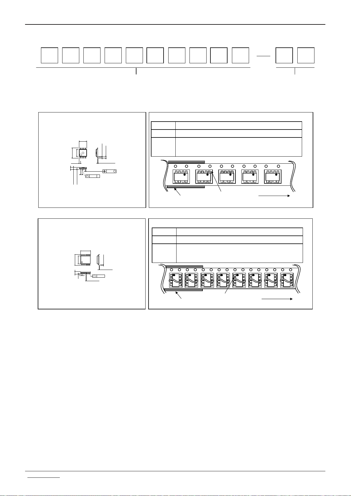
BH76330FVM, BH76331FVM, BH76360FV, BH76361FV,
p
(
y
p
p
BH76332FVM, BH76333FVM, BH76362FV, BH76363FV
●Selection of order type
B
H
7
6
3 3
MSOP8
<Dimension>
4.0 ± 0.2
0.475
0.9Max.
0.75 ± 0.05
0.1
±
2.8
2.9 ± 0.1
0.65
0.08 ± 0.05
58
41
+0.05
0.22
−0.04
0.08 S
BH76330FVM
BH76331FVM
BH76360FV
BH76361FV
0.6 ± 0.2
0.29 ± 0.15
+0.05
0.145
−0.03
0.08
M
Part No.
BH76332FVM
BH76333FVM
BH76362FV
BH76363FV
<Tape and Reel information>
Tape
Quantity
Direction
of feed
SSOP-B16
<Dimension>
(Unit:mm)
6.4 ± 0.3
1.15 ± 0.1
5.0 ± 0.2
0.2
±
4.4
1
0.65
0.1
9816
0.22 ± 0.1
0.3Min.
0.15 ± 0.1
0.1
Unit:mm)
0 F V
Embossed carrier tape
cs
3000
TR
(The direction is the 1pin of product is at the upper right when you hold
reel on the left hand and you pull out the tape on the right hand)
XX
X
X
X X
X
Reel
<Tape and Reel information>
Tape
Quantit
Direction
of feed
Embossed carrier ta
2500
E2
Reel
XX
X
X
X X
X
1Pin
※When you order , please order in times the amount of package quantity.
cs
(The direction is the 1pin of product is at the upper left when you hold
reel on the left hand and you pull out the tape on the right hand)
1pin
※When you order , please order in times the amount of package quantity.
M T R
Tape and Reel information
1234
XX
X
X X
X
X
e
Direction of feed
X X
X
X
X X
X
Direction of feed
1234
X X
X
X X
X
1234
Technical Note
TR
E2
X
1234
www.rohm.com
© 2009 ROHM Co., Ltd. All rights reserved.
32/32
2009.04 - Rev.A
Page 33

Notes
No copying or reproduction of this document, in part or in whole, is permitted without the
consent of ROHM Co.,Ltd.
The content specied herein is subject to change for improvement without notice.
The content specied herein is for the purpose of introducing ROHM's products (hereinafter
"Products"). If you wish to use any such Product, please be sure to refer to the specications,
which can be obtained from ROHM upon request.
Examples of application circuits, circuit constants and any other information contained herein
illustrate the standard usage and operations of the Products. The peripheral conditions must
be taken into account when designing circuits for mass production.
Great care was taken in ensuring the accuracy of the information specied in this document.
However, should you incur any damage arising from any inaccuracy or misprint of such
information, ROHM shall bear no responsibility for such damage.
The technical information specied herein is intended only to show the typical functions of and
examples of application circuits for the Products. ROHM does not grant you, explicitly or
implicitly, any license to use or exercise intellectual property or other rights held by ROHM and
other par ties. ROHM shall bear no responsibility whatsoever for any dispute arising from the
use of such technical information.
Notice
The Products specied in this document are intended to be used with general-use electronic
equipment or devices (such as audio visual equipment, ofce-automation equipment, communication devices, electronic appliances and amusement devices).
The Products specied in this document are not designed to be radiation tolerant.
While ROHM always makes efforts to enhance the quality and reliability of its Products, a
Product may fail or malfunction for a variety of reasons.
Please be sure to implement in your equipment using the Products safety measures to guard
against the possibility of physical injury, re or any other damage caused in the event of the
failure of any Product, such as derating, redundancy, re control and fail-safe designs. ROHM
shall bear no responsibility whatsoever for your use of any Product outside of the prescribed
scope or not in accordance with the instruction manual.
The Products are not designed or manufactured to be used with any equipment, device or
system which requires an extremely high level of reliability the failure or malfunction of which
may result in a direct threat to human life or create a risk of human injury (such as a medical
instrument, transportation equipment, aerospace machiner y, nuclear-reactor controller,
fuel-controller or other safety device). ROHM shall bear no responsibility in any way for use of
any of the Products for the above special purposes. If a Product is intended to be used for any
such special purpose, please contact a ROHM sales representative before purchasing.
If you intend to export or ship overseas any Product or technology specied herein that may
be controlled under the Foreign Exchange and the Foreign Trade Law, you will be required to
obtain a license or permit under the Law.
www.rohm.com
© 2009 ROHM Co., Ltd. All rights reserved.
Thank you for your accessing to ROHM product informations.
More detail product informations and catalogs are available, please contact us.
ROHM Customer Support System
http://www.rohm.com/contact/
R0039
A
 Loading...