

ROHM BH7236AF Datasheet
1
Multimedia ICs
Color TV Signal Encoder
BH7236AF
The BH7236AF converts analog RGB signals into color TV signals in the NTSC and PAL formats. From inputs of
analog RGB signals, a composite synch signal, burst pulses and a color carrier, this IC generates a color TV signal,
and can be adapted for either NTSC or PAL standards, which are selected externally. When set to PAL, chroma
phase is switched for each line.
The chroma signals and luminosity signals can be combined into a color TV signal or output separately, making this
IC suitable for S pins. There are also pins for analog RGB signal output, and each output pin has its own internal
75Ω driver.
•
Applications
TV peripherals
•
Features
1) Can be adapted for NTSC and PAL formats.
2) Internal burst timing signal generator with half-H
killer.
3) Internal flip-flop for PAL phase switching.
4) Separate Y / C output pins.
5) Analog RGB signal output pins.
6) Internal 75Ω driver. (outputs color TV signals, luminosity signals, chroma signals and analog RGB signals)
7) Adaptable for color subcarrier pulse input.
•
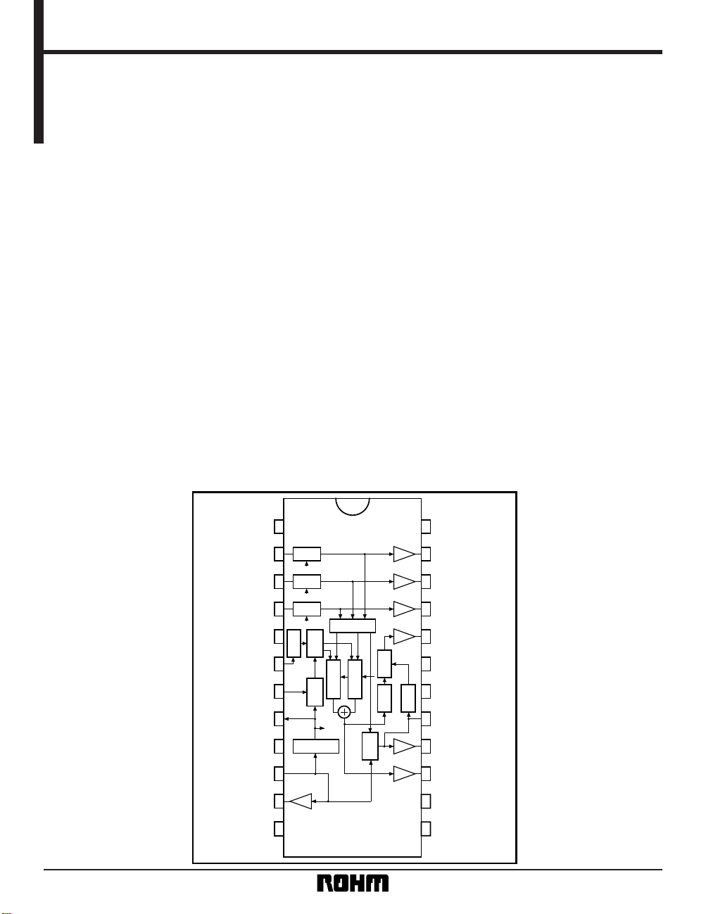
Block diagram
1
2
3
4
5
6
7
8
9
10
11
12
24
23
22
21
20
19
18
17
16
15
14
13
CLAMP
75Ω
75Ω
75Ω
75Ω
75Ω
75Ω
CLAMP
CLAMP
FILTER
PHASE
SIFTER
MATRIX
B-Y MOD.
R-Y MOD.
F · F
Y / C
MIX
BPF
DELAY
SYNC
MIX
BFP GEN.
BFP
BFP
GND2
R
OUT
GOUT
BOUT
VOUT
VCC2
YOUT
COUT
GND1
RIN
GIN
BIN
SCIN
NT / PAL
BFPOUT
SYNCIN
SYNCOUT
V
CC1
N. C.
N. C.
N. C.
N. C.
N. C
YTRAP
SYNC
SYNC
SYNC

2
Multimedia ICs BH7236AF
•
Pin descriptions
Pin name
1 GND1 Ground for all drivers other than the 75
Ω
driver.
2 RIN Analog R signal input. Drive at low impedance.
3 GIN Analog G signal input. Drive at low impedance.
4 BIN Analog B signal input. Drive at low impedance.
5 N. C. This pin is not connected inside the IC.
6 SCIN
7 NT / PAL
8 BFPOUT
9 N. C. This pin is not connected inside the IC.
10 SYNCIN
11 SYNCOUT Composite synchronization signal output.
12
13 N. C. This pin is not connected inside the IC.
14 N. C. This pin is not connected inside the IC.
15 C
OUT
Chroma signal output. Internal 75Ω driver.
16 Y
OUT
Luminance signal output. Internal 75Ω driver.
17 YTRAP
18 N. C. This pin is not connected inside the IC.
19
20 V
OUT
Color TV signal output. Internal 75Ωdriver.
21 B
OUT
Analog B signal output. Internal 75Ω driver.
22 G
OUT
Analog G signal output. Internal 75Ω driver.
23 R
OUT
Analog R signal output. Internal 75Ω driver.
24 GND2 Ground for the 75
Ω
driver.
Power supply pin for all except the 75
Ω
driver.
Power supply pin for the 75
Ω
driver.
Color subcarrier input. Input a 3.579545MHz
(
NTSC) or 4.433619MHz (PAL) sign wave or pulse wave
(50% duty). Do not exceed the range of GND-Vcc.
Burst timing output. Burst timing is generated inside the IC when the subcarrier and composite
synchronization signal.
Selecting the type of color TV signal output. The high level selects NTSC, the low level PAL. Internally
pulled up to 50k
Ω
.
Attached luminance trap filter. Attaching a trap filter reduces chroma signal cross-color caused
by the luminance signal. Output impedance is approximately 2k
Ω
.
Pin No. Function
V
CC1
V
CC2
Composite synchronization signal input. When the low level is input, the synchronization signal is output to
both YOUT and VOUT, and inputs to RIN, GIN and BIN are clamped. This pin is internally pulled up to 100k
Ω
.
 Loading...