

Page 1

A
System Lens Driver Series for Mobile Phone Cameras
2-wire serial interface
Lens Driver for Voice Coil Motor
(I2C BUS compatible)
BH6456GUL
●General Description
The BH6456GUL motor driver provide 1 Full on Driver a
H-bridge.
This lens driver is offered in an ultra-small functional lens
system for use in an auto focus system using a Piezo
actuator.
●Features
Ultra-small chip size package .
Low ON-Resistance Power CMOS output.
Built-in 15MHz Oscillator
Built-in UVLO (Under Voltage Locked Out: UVLO).
Built-in TSD (Thermal Shut Down) circuit.
Standby current consumption: 0μA Typ.
1.8V can be put into each control input terminal
●Applications
For Auto focus of camera module
Digital still camera
Camera Modules
Lens Auto focus
Web Cameras
●Typical Application Circuit(s)
SDA
SCL
2-wire
Serial
Interface
TSD
UVLO
PS
Controller
15MHz
OSC
Pre
Driver
Fig.1 Block Diagram
○Product structure:Silicon monolithic integrated circuit ○This product is not designed protection against radioactive rays
●Key Specifications
Pch ON Resistance: 0.70Ω(Typ.)
Nch ON Resistance: 0.70Ω(Typ.)
Standby current consumption: 0μA (Typ.)
15MHz OSC: ±3.0%
Operating temperature range: -25℃ to +85℃
●Package(s) W(Typ.) x D(Typ.) x H(Max.)
VCSP50L1 1.95mm x 1.00mm x 0.55mm
VCC
Band
Gap
VREG
VM
OUTA
H Bridge
OUTB
GND
No.12015EAT03
www.rohm.com
© 2012 ROHM Co., Ltd. All rights reserved.
1/19
2012.03 - Rev.
Page 2
BH6456GUL
A
Technical Note
● Absolute maximum ratings (Ta=+25°C)
Parameter Symbol Limit Unit
Power supply voltage VCC -0.3 to +4.5 V
Motor power supply voltage VM -0.3 to +5.5 V
Power save input voltage VPS
-0.3 to VCC+0.3 V
Control input voltage VIN -0.3 to VCC+0.3 V
Power dissipation Pd 530*1 mW
Operating
temperature range
Topr -25 to +85 °C
Junction temperature Tjmax +125 °C
Storage temperature range Tstg -55 to +125 °C
H-bridge output current Iout -500 to +500*2 mA
*1
Conditions: mounted on a glass epoxy board (50mm 58mm 1.75mm; 8 layers). In case of Ta>25°C, reduced by 5.3 mW/°C.
*2
Must not exceed Pd, ASO, or Tjmax of 125°C.
●Operating Conditions (Ta= -25°C to +85°C)
Parameter Symbol Min. Typ. Max. Unit
Power supply voltage VCC 2.3 3.0 3.6 V
Motor power supply voltage VM 2.3 3.0 4.8 V
Power save input voltage VPS
Control input voltage VIN
2-wire serial interface transmission rate SCL
0 - VCC V
0 - VCC V
- - 400 kHz
H-bridge output current Iout - - 400*3 mA
*3
Must not exceed Pd, ASO.
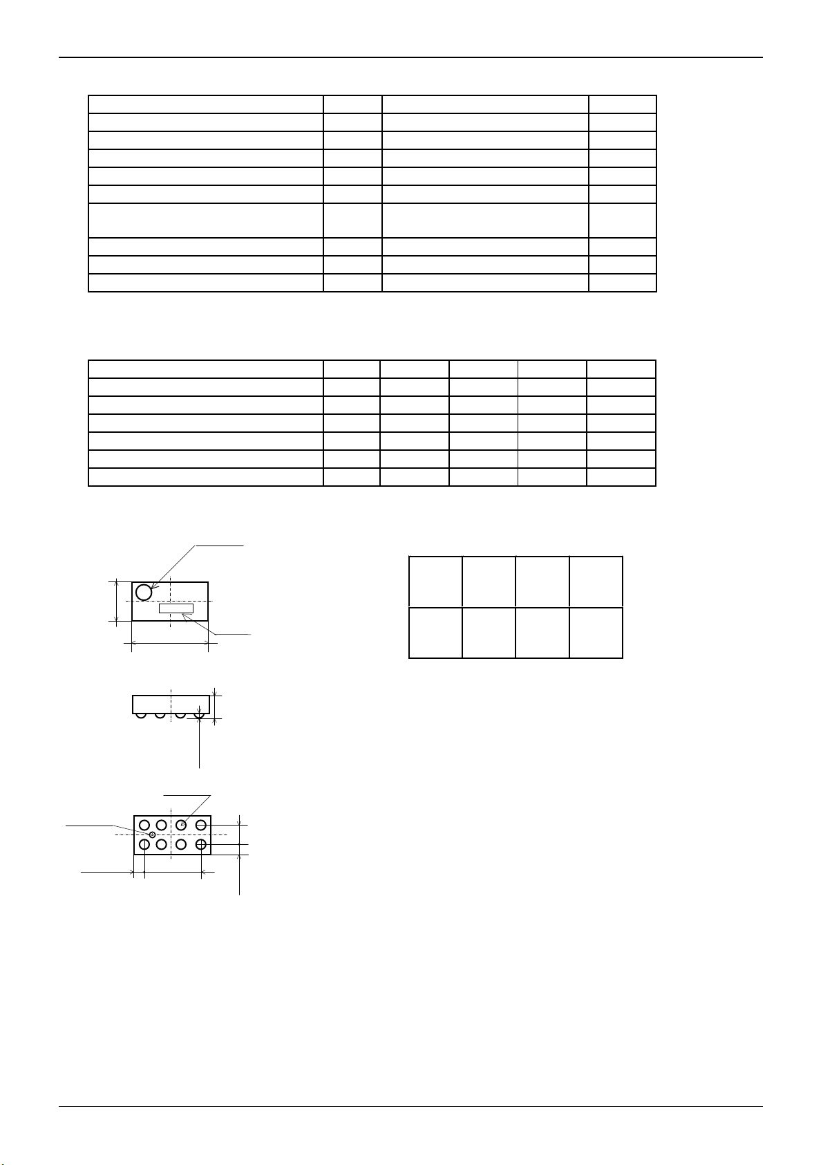
Package Outline Pin Arrangement (Top View)
1PIN MARK
1 2 3 4
AAU
(φ0.15)
INDEX POST
0.225±0.05
1.0±0.05
1.95±0.05
φ0.25±0.1
P=0.5×3
Lot No.
0.55MAX
0.1±0.05
P=0.5×1
0.25±0.05
Fig.2 VCSP50L1 Package (Unit: mm)
AVM OUTB SCL SDA
Top View
B OUTA GND VCC PS
Fig.3 Pin Arrangement (Top View)
Side View
Bottom View
www.rohm.com
© 2012 ROHM Co., Ltd. All rights reserved.
2/19
2012.02 - Rev.
Page 3

BH6456GUL
A
● Electrical Characteristics (Unless otherwise specified Ta=25°C, VCC=3.0V )
Parameter Symbol
Min. Typ. Max.
Limit
Unit Conditions
Overall
Circuit current
during standby operation
ICCST - 0 1
μA
PS=L
Circuit current ICC - 3.2 6.4 mA PS=H, SCL=400kHz, OSC active
UVLO
UVLO voltage VUVLO 1.8 - 2.2 V
Power save input
High level input voltage VPSH 1.5 - VCC V
Low level input voltage VPSL 0 - 0.5 V
High level input current
Low level input current
IPSH
IPSL
15 30 60 μA VINH=3.0V
-3 0 - μA VINL=0V
Control input(SDA,SCL)
High level input voltage
Low level input voltage
Low level output voltage
High level input current
Low level input current
VINH
VINL
VOL
IINH
IINL
1.5 - VCC V
0 - 0.5 V
- - 0.4 V IIN=3.0mA (SDA)
-10 - 10 μA Input voltage=VCC
-10 - 10 μA Input voltage=GND
H Bridge Drive
Ω
Output ON-Resistance
Cycle length of
sequence drive
RONP - 0.7 1.0
RONN - 0.7 1.0
TMIN 10.35 10.67 11.00 μs*4 Built in CLK 160 count
Output rise time Tr - 0.1 0.8 μs
Output fall time Tf - 0.02 0.4 μs
*4
The time that 1 cycle of sequence drive at the below setting of 2-wire serial data
*5
Output switching wave
ta[7:0] = 0x13, brake1[7:0] = 0x03, tb[7:0] = 0x1E, brake2[7:0] = 0x6B, osc[2:0] = 0x0
Ω
*5
7.5Ω load condition
*5
7.5Ω load condition
Output
voltage
90%
10%
10%
Tf Tr
90%
100
0%
Technical Note
www.rohm.com
© 2012 ROHM Co., Ltd. All rights reserved.
3/19
2012.02 - Rev.
Page 4

BH6456GUL
A
Technical Note
●2 wire Serial Interface Register detail
Write mode :S 0 0 0 1 1 0 0 0 A PST2T1T0W3W2W1W0 A D7D6D5D4D3D2D1D0 A P Master is output
Read mode :S00011000APST2T1T0W3W2W1W0AS00011001AD7D6D5D4D3D2D1D0nA P
S=Start condition A=Acknowledge PS=Power save W3~W0=Resister address
P=Stop condition nA=not Acknowledge T2~T0=Test bit D7~D0=Data
↑ ↑
Write Up date Slave is output
↑ ↑
Write Read
●Resister
Address W3 W2 W1 W0 D7 D6 D5 D4 D3 D2 D1 D0
0H 0 0 0 0 HiZE initB[2] initB[1] InitB[0] init START MODE dir
1H 0 0 0 1 ta[7] ta[6] ta[5] ta[4] ta[3] ta[2] ta[1] ta[0]
2H 0 0 1 0 brake1[7] brake1[6] brake1[5] brake1[4] brake1[3] brake1[2] brake1[1] brake1[0]
3H 0 0 1 1 tb[7] tb[6] tb[5] tb[4] tb[3] tb[2] tb[1] tb[0]
4H 0 1 0 0 brake2[7] brake2[6] brake2[5] brake2[4] brake2[3] brake2[2] brake2[1] brake2[0]
5H 0 1 0 1 cnt[7] cnt[6] cnt[5] cnt[4] cnt[3] cnt[2] cnt[1] cnt[0]
6H 0 1 1 0 cnt[15] cnt[14] cnt[13] cnt[12] cnt[11] cnt[10] cnt[9] cnt[8]
7H 0 1 1 1 pa pb osc[2] osc[1] osc[0] cntck[2] cntck[1] cntck[0]
8H 1 0 0 0 TEST TEST TEST TEST TEST TEST TEST TEST
9H 1 0 0 1 TEST TEST TEST TEST TEST TEST TEST TEST
AH 1 0 1 0 TEST TEST TEST TEST TEST TEST EXT initEXT
BH 1 0 1 1 TEST TEST TEST TEST TEST TEST TEST TEST
CH 1 1 0 0 TEST TEST TEST TEST TEST TEST TEST TEST
www.rohm.com
© 2012 ROHM Co., Ltd. All rights reserved.
4/19
2012.02 - Rev.
Page 5
BH6456GUL
A
Technical Note
●2 wire Serial Interface Action Timing Characteristics (Unless otherwise specified, Ta=-25 to +85°C, VCC=2.3 to 4.8V)
Parameter Symbol
FAST-MO DE*6 STANDARD-MODE*6
Min. Typ. Max. Min. Typ. Max.
SCL frequency fSCL - - 400 - - 100 kHz
Data clock high time tHIGH 0.6 - - 4.0 - - μs
Data clock low time tLOW 1.3 - - 4.7 - - μs
Start condition hold time tHD:STA 0.6 - - 4.0 - - μs
Start condition setup time tSU:STA 0.6 - - 4.7 - - μs
Data hold time tHD:DAT 0 - 0.9 0 - 3.45 μs
Data setup time tSU:DAT 100 - - 250 - - ns
Stop condition setup time tSU:STO 0.6 - - 4.0 - - μs
BUS release time tBUF 1.3 - - 4.7 - - μs
Noise removal valid period tI 0 - 50 0 - 50 ns
*6
Standard-mode and Fast-mode 2-wire serial interface devices must be able to transmit or receive at that speed.
The maximum bit transfer rates of 100 kbit/s for Standard-mode devices and 400 kbit/s for Fast-mode devices
This transfer rates is provided the maximum transfer rates, for example it is able to drive 100 kbit/s of clocks with Fast-mode.
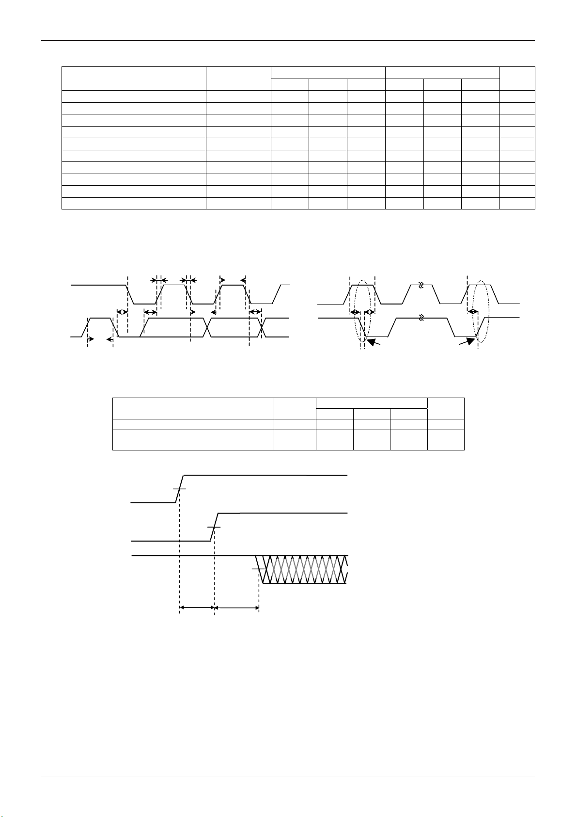
●2 wire Serial Interface Data timing
SCL
SDA
tHD : STA
tBUF
tR
tF
tSU : DAT
tLOW
tHIGH
tHD : DAT
SCL
SDA
tSU : STA
tHD : STA
START BIT
tSU : STO
STOP BIT
Fig.4 Serial data timing Fig.5 Start stop bit timing
●Recommend to power supply turning on operation timing
Parameter Symbol
Recommendation limit
Min. Typ. Max.
Unit
PS input H voltage set-up time TPS 1 - - us
2-wire serial interface input data set-up
time
tI2C 1 - - us
●Sequence of data input timing to power supply
VCC,VM
50%
PS
50%
2-wire serial input
50%
Serial data
Unit
www.rohm.com
© 2012 ROHM Co., Ltd. All rights reserved.
tPS tI2C
5/19
2012.02 - Rev.
Page 6

BH6456GUL
A
●Driving wave setting
○ The structure of the driving wave for SIDM
1cycle=(ta+1)+brake1+tb+brake2
Technical Note
Ⅰ Ⅱ
1osc 1osc1osc1osc 1osc1osc
Ⅲ Ⅳ Ⅴ Ⅵ
Ⅶ
①
②
ta+1
Ⅱcw(ccw) Ⅵ CCW(cw)
*1
Ⅰ.HiZ
*1
The state at A or B and C is HiZ.
*2
At mode=0,the output logic is a setting of a short brake.
dir(address:OH,D2) ① ② Note
Driving wave is set by the 4 parameters of ta / brake1 / tb / brake2.
osc period is set by the osc(Internal CLK basic cycle setting).
ta : On section is ( ta +1-1) = ta counts for cw(ccw) state.
brake1 : On section is (brake1 -1) count for short brake state.
tb : On section is (tb1 -1) count for ccw(cw) state.
brake2 : On section is (brake2 -1) count for short brake state.
(Ex.) In case of setting 1 cycle = 10.67
osc[2:0]( = Basic cycle setting ) = 3’b000( = Basic cycle = 66.67ns)、and ta / brake1 / tb / brake2 setting below;
brake1
*1
ⅢHiZ
Ⅴ HiZ
Ⅳ Short brake
tb
*1
*2
Ⅶ HiZ
*1
0 OUTA OUTB Move to the direction of Macro
1 OUTB OUTA Move to the direction of ∞
μs、ta = 1.27μs、brake1 = 0.13μs、tb = 1.93μs, brake2 = 7.07μs.
ta[7:0] = 0x13 = 19 count → ON section = 19+1-1= 19 count
brake1[7:0] = 0x03 = 3 count → ON section = 2 count
tb[7:0] = 0x1E = 30 count → ON section = 29 count
brake2[7:0] = 0x6B = 107 count → ON section = 106 count
Ⅷ
brake2
Ⅷ Short brake
*2
CW:Forward rotation
CCW:Reverse rotation
Ⅰ Ⅱ Ⅲ
ta
Ⅱ cw(ccw)
*1
Ⅰ HiZ
Ⅲ HiZ
*1
www.rohm.com
© 2012 ROHM Co., Ltd. All rights reserved.
6/19
2012.02 - Rev.
Page 7

BH6456GUL
A
○ Driver function table
Sequence setting
mode = 0, osc = 0x0 or osc≠0x0 and HiZE = 0
Ⅰ Ⅱ Ⅲ Ⅳ Ⅴ Ⅵ Ⅶ Ⅷ
Technical Note
output①
output②
mode HiZ CW HiZ
HiZ H HiZ L L L L L
L L L L HiZ H HiZ L
Short
brake
HiZ CCW HiZ
mode = 0, osc≠0x0 and HiZE = 1
output①
output②
mode
*3 The output ② status of Ⅶ dosen’t become from HiZ(66.67nsec) to Low.It is outputted HiZ.
Ⅰ Ⅱ Ⅲ Ⅳ Ⅴ Ⅵ Ⅶ Ⅷ
HiZ(66.67ns
ec)→H
L L L L
HiZ(66.67ns
ec)→CW
H
CW
HiZ(66.67ns
ec)→L
HiZ(66.67ns
ec)→Short
brake
L L L L L
Short
brake
HiZ(66.67ns
ec)→H
HiZ(66.67ns
ec)→CCW
H HiZ*3 L
CCW HiZ*3
mode = 1, osc = 0x0 or osc≠0x0 and HiZE = 0
output①
output②
mode HiZ CW HiZ HiZ HiZ CCW HiZ HiZ
Ⅰ Ⅱ Ⅲ Ⅳ Ⅴ Ⅵ Ⅶ Ⅷ
HiZ H HiZ HiZ L L L HiZ
L L L HiZ HiZ H HiZ HiZ
mode = 1, osc≠0x0 and HiZE = 1
Ⅰ Ⅱ Ⅲ Ⅳ Ⅴ Ⅵ Ⅶ Ⅷ
Short
brake
Short
brake
output①
output②
mode
*4 The output ① status of Ⅶ dosen’t become from Low (66.67nsec) to HiZ .It is outputed Low.
HiZ(66.67ns
ec)→H
L L
HiZ(66.67ns
ec)→CW
H HiZ HiZ
L(66.67nsec
)→HiZ
CW HiZ HiZ
HiZ
HiZ(66.67ns
HiZ(66.67ns
HiZ(66.67ns
ec)→CCW
Truth table of Pa and Pb
sequence pa pb OUTA OUTB Function mode
OFF 0 0 Z Z STOP
OFF 0 1 L H CCW
OFF 1 0 H L CW
OFF 1 1 L L Short brake
ON X x - - Follow with the sequence
ec)→L
ec)→H
L L*4 HiZ
H HiZ HiZ
CCW HiZ HiZ
www.rohm.com
© 2012 ROHM Co., Ltd. All rights reserved.
7/19
2012.02 - Rev.
Page 8

BH6456GUL
A
○Normal sequence
Setting ta[7:0], brake1[7:0], tb[7:0], brake2[7:0], osc[2:0], HiZE, pa, pb, cntck[2:0], cnt[15:0]
input data
START
START = Hi → Lo while normal sequence, stop the sequence
input data
dir
Macro direction select
direction select
∞
1cycle
OUTA
OUTB
output data
EXT
Internal Counter
Count up
set
value
Reset
Count up
Reset
Move to Macro direction (movement at set cycle)
Normal sequence
input data
START
Set output logic by
pa , pb
In this case of short brake
In the case of dir = Lo → Hi or Hi → Lo input while
START=Hi,reset setting cycle,and start normal
Normal sequence
Move to ∞ to direction
Set output logic by
pa , pb
input data
dir
Macro direction select
∞ direction select
Technical Note
1cycle
OUTA
OUTB
output data
EXT
Internal Counter
Count up Count up
Normal sequence
Move to macro direction
www.rohm.com
© 2012 ROHM Co., Ltd. All rights reserved.
set
value
Normal sequence
Move to macro direction
8/19
set value
see output logic by pa,pb
2012.02 - Rev.
Page 9

BH6456GUL
A
○Initial sequence
Setting ta[7:0], brake1[7:0], tb[7:0], brake2[7:0], osc[2:0], HiZE, pa, pb, cntck[2:0], cnt[15:0], initB[2:0]
Count stop
Stop squence
I2C input data
I2C input data
I2C output data
Internal Counter
START
init
initEXT
reset
reset reset
set
output
set
output
∞dir
N ormal sequence
Count up
∞ direction
direction
∞
Setting value
m
Count up Count up Count up Count up
set
Normal sequence
output
reset
set
output
∞ dir
Technical Note
S et output logic by
pa
, pb(I2C)
Move to ∞ direction
Ignore dir(I2C) signal
I2C input data
START
I2C input data
I2C output data
initEXT
Internal Counter
init
Initial sequence
Move to macro direction
setting initB[2:0]
(
Count up
Count up
∞ direction
In the case of init(I2C)= Hi→Lo input
while START(I2C)=Lo,initEXT=Hi
Lo output.
)
direction
∞
Setting value
Count up Count up
set
m
output
Normal sequence
In the case of initial(I2C)= Hi→Lo
input while initial sequence, res et
→
setting c ycle, and obey output
logic by pa,pb(I2C).
reset
set
output
Normal sequence
In the case of START(I2C)=Lo
input while initial sequence, res et
setting cycle, and start normal
sequence.
reset
Count up
set
∞ dir m
output
∞ direction
Setting value
Set output logic by
pa,pb(I2C)
Hi
→
reset
www.rohm.com
© 2012 ROHM Co., Ltd. All rights reserved.
Initial sequence
At START(I2C)=Hi,it is initEXT(I2C)=Hi
regardless of the init(I2C) logic
Initial sequence
In the case of initEXT(I2C)=Hi
output at init(I2C)=Hi
sequence ends.
9/19
Lo after initial
→
→
2012.02 - Rev.
Lo
Page 10

BH6456GUL
A
○STOP sequence
It changes to the next state after short brake 16.7
shown in the following while the sequence is operating is done.
・ When Initial sequence ∞ direction ends
・ When Initial sequence ends
・ When normal sequence ends
・ When dir bit signal reversing input is done at START bit = H
・ When initial sequence cancels
・ When normal sequence cancels
・ When the normal sequence interrupts at an initial sequence
○ Output rise, fall waveform
μsec(typ) when the state transition
Technical Note
VM
(VM-B)*0.9+B
Output
voltage
A*0.9
A*0.1
A
Trise
Tfall
(VM-B)*0.1+B
B
0V
Output
current
A voltage = (VM voltage) – (Simulation DC output current at the only Resistance load) ×(Upper side output On-R)
B voltage = (Simulation DC output current at the only Resistance load) × (Lower side output On-R)
(Ex.) In case, the load is Resistance element = 2Ω, capacity element = 0.033
A voltage = (VM voltage) – ((VM voltage)÷(Load (R)+ Total ON-R))×(Upper side ON-R)
= 3V – (3V÷(2Ω+(1Ω+1Ω)))×1Ω
= 2.25V
B voltage = ((VM voltage)÷(Load (R)+ Total ON-R))×(Lower side ON-R)
= (3V÷(2Ω+(1Ω+1Ω)))×1Ω
= 0.75V
0mA
μF
25°C, VM=3V, Upper side output On-R = 1Ω, Lower side output On-R = 1Ω
Rise time = Trise (A×0.1 to A×0.9) = 100nsec(typ)
Fall time = Tfall ((VM-B)×0.9+B to (VM-B)×0.1+B) = 100nsec(typ)
www.rohm.com
© 2012 ROHM Co., Ltd. All rights reserved.
10/19
2012.02 - Rev.
Page 11

BH6456GUL
A
●Register detail
○Register catalogue
Bit BIT Name Function
address : 0H
D0 dir Output direction setting while normal sequence
D1 MODE Mode of brake1/brake2 setting for initial/normal sequence
D2 START Start setting for normal sequence
D3 init Start setting for initial sequence
D4 Initb[0] Macro direction setting while initial sequence[0]
D5 Initb[1] Macro direction setting while initial sequence [1]
D6 Initb[2] Macro direction setting while initial sequence [2]
D7 HiZE
address : 1H
D0 ta[0] Drive waveform setting[0] ta
D1 ta[1] Drive waveform setting[1] ta
D2 ta[2] Drive waveform setting[2] ta
D3 ta[3] Drive waveform setting[3] ta
D4 ta[4] Drive waveform setting[4] ta
D5 ta[5] Drive waveform setting[5] ta
D6 ta[6] Drive waveform setting[6] ta
D7 ta[7] Drive waveform setting[7] ta
address : 2H
D0 brake1[0] Drive waveform setting[0] brake1
D1 brake1[1] Drive waveform setting[1] brake1
D2 brake1[2] Drive waveform setting[2] brake1
D3 brake1[3] Drive waveform setting[3] brake1
D4 brake1[4] Drive waveform setting[4] brake1
D5 brake1[5] Drive waveform setting[5] brake1
D6 brake1[6] Drive waveform setting[6] brake1
D7 brake1[7] Drive waveform setting[7] brake1
address : 3H
D0 tb[0] Drive waveform setting[0] tb
D1 tb[1] Drive waveform setting[1] tb
D2 tb[2] Drive waveform setting[2] tb
D3 tb[3] Drive waveform setting[3] tb
D4 tb[4] Drive waveform setting[4] tb
D5 tb[5] Drive waveform setting[5] tb
D6 tb[6] Drive waveform setting[6] tb
D7 tb[7] Drive waveform setting[7] tb
Dead time setting (Lo: 1 cycle of osc[2:0] setting、 Hi: Internal CLK 1 cycle (typ
66.67nsec)
Technical Note
www.rohm.com
© 2012 ROHM Co., Ltd. All rights reserved.
11/19
2012.02 - Rev.
Page 12

BH6456GUL
A
Bit BIT Name Function
address : 4H
D0 brake2[0] Drive waveform setting[0] brake2
D1 brake2[1] Drive waveform setting[1] brake2
D2 brake2[2] Drive waveform setting[2] brake2
D3 brake2[3] Drive waveform setting[3] brake2
D4 brake2[4] Drive waveform setting[4] brake2
D5 brake2[5] Drive waveform setting[5] brake2
D6 brake2[6] Drive waveform setting[6] brake2
D7 brake2[7] Drive waveform setting[7] brake2
address : 5H
D0 cnt[0] Drive time count setting[0]
D1 cnt[1] Drive time count setting[1]
D2 cnt[2] Drive time count setting[2]
D3 cnt[3] Drive time count setting[3]
D4 cnt[4] Drive time count setting[4]
D5 cnt[5] Drive time count setting[5]
D6 cnt[6] Drive time count setting[6]
D7 cnt[7] Drive time count setting[7]
address : 6H
D0 cnt[8] Drive time count setting[8]
D1 cnt[9] Drive time count setting[9]
D2 cnt[10] Drive time count setting[10]
D3 cnt[11] Drive time count setting[11]
D4 cnt[12] Drive time count setting[12]
D5 cnt[13] Drive time count setting[13]
D6 cnt[14] Drive time count setting[14]
D7 cnt[15] Drive time count setting[15]
address : 7H
D0 cntck[0] Drive time basic cycle setting[0]
D1 cntck[1] Drive time basic cycle setting [1]
D2 cntck[2] Drive time basic cycle setting [2]
D3 osc[0] Internal CLK basic cycle setting[0]
D4 osc[1] Internal CLK basic cycle setting [1]
D5 osc[2] Internal CLK basic cycle setting [2]
D6 pb Output logic setting b
D7 pa Output logic setting a
Technical Note
www.rohm.com
© 2012 ROHM Co., Ltd. All rights reserved.
12/19
2012.02 - Rev.
Page 13

BH6456GUL
A
Bit BIT Name Function
address : 8H
D0 cntout[0] Drive time count value output[0]
D1 cntout[1] Drive time count value output[1]
D2 cntout[2] Drive time count value output[2]
D3 cntout[3] Drive time count value output[3]
D4 cntout[4] Drive time count value output[4]
D5 cntout[5] Drive time count value output[5]
D6 cntout[6] Drive time count value output[6]
D7 cntout[7] Drive time count value output[7]
address : 9H
D0 cntout[8] Drive time count value output[8]
D1 cntout[9] Drive time count value output[9]
D2 cntout[10] Drive time count value output[10]
D3 cntout[11] Drive time count value output[11]
D4 cntout[12] Drive time count value output[12]
D5 cntout[13] Drive time count value output[13]
D6 cntout[14] Drive time count value output[14]
D7 cntout[15] Drive time count value output[15]
address : AH
D0 initEXT After initial sequence, Hi output
D1 EXT Hi output while normal sequence、Lo output at the stop mode
D2 TEST
D3 TEST
D4 TEST
D5 TEST
D6 TEST
D7 TEST
address : BH
D0 TEST
D1 TEST
D2 TEST
D3 TEST
D4 TEST
D5 TEST
D6 TEST
D7 TEST
address : CH
D0 TEST
D1 TEST
D2 TEST
D3 TEST
D4 TEST
D5 TEST
D6 TEST
D7 TEST
Technical Note
www.rohm.com
© 2012 ROHM Co., Ltd. All rights reserved.
13/19
2012.02 - Rev.
Page 14

BH6456GUL
A
○Internal CLK basic cycle setting [osc] Internal CLK 1 cycle = 66.67nsec(typ)
Magnificati
on
3’b000 1 3’b010 3 3’b100 5 3’b110 7
3’b001 2 3’b011 4 3’b101 6 3’b111 8
Internal
CLK cycle
number
Magnificati
on
Internal
CLK cycle
number
Magnificati
on
Internal
CLK cycle
number
○Drive waveform [ta, brake1, tb, brake2]
Osc
Time setting
8’b0000_0000 1 8’b0100_0000 64 8’b1000_0000 128 8’b1100_0000 192
8’b0000_0001 1 8’b0100_0001 65 8’b1000_0001 129 8’b1100_0001 193
8’b0000_0010 2 8’b0100_0010 66 8’b1000_0010 130 8’b1100_0010 194
8’b0000_0011 3 8’b0100_0011 67 8’b1000_0011 131 8’b1100_0011 195
… … … … … … … …
8’b0011_1101 61 8’b0111_1101 125 8’b1101_1101 189 8’b1111_1101 253
8’b0011_1110 62 8’b0111_1110 126 8’b1101_1110 190 8’b1111_1110 254
8’b0011_1111 63 8’ b0 111_1111 127 8’b1101_1111 191 8’b1111 _1111 255
Cycle
number
Time setting
Osc
Cycle
number
Time setting
Osc
Cycle
number
○Drive time basic cycle setting [cntck]
Magnificati
on
Cycle
number
Magnificati
on
Cycle
number
Magnificati
on
Cycle
number
Magnificati
on
Time setting
Magnificati
on
Technical Note
Internal
CLK cycle
number
Osc
Cycle
number
Cycle
number
3’b000 1 3’b010 4 3’b100 15 3’b110 64
3’b001 2 3’b011 8 3’b101 32 3’b111 127
www.rohm.com
© 2012 ROHM Co., Ltd. All rights reserved.
14/19
2012.02 - Rev.
Page 15

BH6456GUL
A
○Macro direction setting while initial sequence [initB] ( (Total count number) = (cntck)×(initB))
count
setting
3’b000 1 3’b010 4 3’b100 15 3’b110 64
3’b001 2 3’b011 8 3’b101 32 3’b111 127
Cntck cycle
number
count
setting
Cntck cycle
number
count
setting
Cntck cycle
number
count
setting
○Drive time count setting [cnt] ( (Total Drive count number) = (cntck)×(cnt))
count setting Cntck cycle
number
16’h0000 1 16’h4000 16384 16’h8000 32768 16’hC000 49152
16’h0001 1 16’h4001 16385 16’h8001 32769 16’hC001 49153
16’h0002 2 16’h4002 16386 16’h8002 32770 16’hC002 49154
16’h0003 3 16’h4003 16387 16’h8003 32771 16’hC003 49155
… … … … … … … …
16’h3FFD 16381 16’h7FFD 32765 16’hBFFD 49149 16’hFFFD 65533
16’h3FFE 16382 16’h7FFE 32766 16’hBFFE 49150 16’hFFFE 65534
16’h3FFF 16383 16’h7FFF 32767 16’hBFFF 49151 16’hFFFF 65535
count setting Cntck cycle
number
count
setting
Cntck cycle
number
count
setting
(Ex.) In case, setting cntck[2:0] = 3’b001, cnt[15:0] = 16’h8000
cntck×cnt = 2×32768
= 65536count
= 851.968msec (In case of setting a cycle = 13usec)
Technical Note
Cntck cycle
number
Cntck
cycle number
www.rohm.com
© 2012 ROHM Co., Ltd. All rights reserved.
15/19
2012.02 - Rev.
Page 16

BH6456GUL
A
●I/O Peripheral Circuit
1) Pull up resistance of SDA terminal
SDA is NMOS open drain, so requires pull up resistance. As for this resistance value (RPU), select an appropriate
value to this resistance value from micro-controller V
action frequency is limited. The smaller the R
, the larger the consumption current at action.
PU
, IL, and VOL – IOL characteristics of this IC. If RPU is large,
IL
2) Maximum value of R
The maximum value of R
PU
is determined by the following factors.
PU
(Ⅰ)SDA rise time to be determined by the capacity (CBUS) of BUS line of R
And AC timing should be satisfied even when SDA rise time is late.
(Ⅱ)The BUS electric potential V
to be determined by input leak total (IL) of device connected to BUS at output of “H” to
1
SDA BUS and RPU should sufficiently secure the input “H” level (VIH) of micro-controller and driver including
recommended noise margin 0.2VCC.
VCC - I
Example.) VCC = 3V, I
- 0.2×VCC ≧ VIH
L×RPU
∴R
≦ ・・・・・①
PU
0.8×VCC - VIH
L
I
=10μA, V
L
= 0.7×VCC
IH
from ①
0.8×3 - 0.7×3
R
≦ = 30kΩ
PU
10×10-6
3) Minimum value of R
The minimum value of R
(Ⅰ)When IC outputs LOW, it should be satisfied that V
VCC-VOL
(Ⅱ)V
= 0.4V should secure the input “L” level (VIL) of micro-controller and driver including recommended noise
OLMAX
Fig.6 2 wire Serial Interface 1
PU
is determined by the following factors.
PU
= 0.4V, and I
OLMAX
≦ I
・・・・・②
OL
RPU
margin 0.1VCC.
V
≦ VIL-0.1×VCC
OLMAX
Ex.) VCC = 3V, V
≧ = 867[Ω]
R
PU
And V
= 0.4[V], V
OL
=0.4V, I
OL
OL
3 - 0.4
-3
3×10
= 0.3×3 = 0.9[V]
IL
= 3mA, micro-controller, driver V
IL
Therefore, the condition (Ⅱ) is satisfied.
4) Pull up resistance of SCL terminal
WHEN SCL control is made at CMOS output port, there is no need but in the case there is timing where SCL
becomes “Hi-Z”, add a pull up resistance. As for the pull up resistance, one of several kΩ to several ten kΩ is
recommended in consideration of drive performance of output port of micro-controller.
PU
Micro-controller
OLMAX
= 0.3×VCC
Technical Note
and SDA should be tR or below.
IL
= 3mA.
RPU
V1
Bus line capacity
CBUS
IL
BR24LX
SDA terminal
www.rohm.com
© 2012 ROHM Co., Ltd. All rights reserved.
16/19
2012.02 - Rev.
Page 17

BH6456GUL
A
A
Technical Note
●Cautions on Micro-controller Connection
1) R
s
In the 2 wire Serial Interface, it is recommended that SDA port is of open drain input/output. However, when to use
CMOS input / output of tri state to SDA port, inset a series resistance R
between the pull up resistance Rpu and the
s
SDA terminal of driver. This controls over current that occurs when PMOS of the micro-controller and NMOS of driver
are turned ON simultaneously. R
when SDA port is open drain input/output, R
also plays the role of protection of SDA terminal against surge. Therefore, even
s
can be used.
s
CK
Micro-controller
Fig.7 2 wire Serial Interface 2 Fig.8 Input / Output collision timing
2) Maximum value of R
s
The maximum value of Rs is determined by the following relations.
(Ⅰ)SDA rise time to be determined by the capacity (C
And AC timing should be satisfied even when SDA rise time is late.
(Ⅱ)The BUS electric potential V
should sufficiently secure the input “L” level (V
V
IL
3) Minimum value of R
Fig.10 2 wire Serial Interface 4
micro-controller
Fig.9 2 wire Serial Interface 3 R
S
The minimum value of R
source line, and instantaneous power failure of power source may occur. When allowable over current is defined as I,
the following relation must be satisfied. Determine the allowable current in consideration of impedance of power
source line in set and so forth. Set the over current to driver 10mA or below.
VCC
R
S
Exampre) When VCC=3V, I=10mA, From ④
≧ =300[Ω]
R
s
RPU
Rs
Driver
SCL
H output of micro-controller
SDA
L output of Driver
Over current flows to SDA line by H output of micro-controller
and L output of Driver
) of BUS line of Rpu and SDA should be tR or below.
b
to be determined by Rpu and Rs at the moment when driver outputs “L” to SDA BUS
2
) of micro-controller including recommended noise margin 0.1VCC.
IL
VCC
R
PU
Bus line
capacity
C
b
V2
Rs
IOL
VOL
(VCC-VOL)×RS
R
PU+RS
∴Rs ≦ ×RPU ・・・・③
VIL-VOL-0.1×VCC
1.1×VCC-V
Example) When VCC = 3V, V
+0.1×VCC ≦ VIL
+V
OL
IL
= 0.3×VCC, V
IL
= 0.4V, R
OL
from ③
driver
0.3×3 - 0.4 - 0.1×3
≦ ×20×103 = 1.67[kΩ]
s
is determined by over current at BUS collision. When over current flows, noises in power
s
≦ I ・・・・④
3
1.1×3 - 0.3×3
RPU
RS
Over current I
10×10-3
H output
Microcontroller
= 20kΩ,
PU
Driver
L output
www.rohm.com
© 2012 ROHM Co., Ltd. All rights reserved.
17/19
2012.02 - Rev.
Page 18

BH6456GUL
A
●Operation Notes
1) Absolute maximum ratings
Use of the IC in excess of absolute maximum ratings, such as the applied voltage (VCC) or operating temperature
range (Topr), may result in IC damage. Assumptions should not be made regarding the state of the IC (short mode or
open mode) when such damage is suffered. A physical safety measure, such as a fuse, should be implemented
when using the IC at times where the absolute maximum ratings may be exceeded.
2) Storage temperature range (Tstq)
As long as the IC is kept within this range, there should be no problems in the IC’s performance. Conversely,
extreme temperature changes may result in poor IC performance, even if the changes are within the above range.
3) Power supply and wiring
Be sure to connect the power terminals outside the IC. Do not leave them open. Because a return current is
generated by a counter electromotive force of the motor, take necessary measures such as putting a Capacitor
between the power source and the ground as a passageway for the regenerative current. Be sure to connect a
Capacitor of proper capacitance (0.1μF to 10μF) between the power source and the ground at the foot of the IC, and
ensure that there is no problem in properties of electrolytic Capacitors such as decrease in capacitance at low
temperatures. When the connected power source does not have enough current absorbing capability, there is a
possibility that the voltage of the power source line increases by the regenerative current an exceeds the absolute
maximum rating of this product and the peripheral circuits.
Therefore, be sure to take physical safety measures such as putting a zener diode for a voltage clamp between the
power source an the ground.
4) Ground terminal and wiring
The potential at GND terminals should be made the lowest under any operating conditions. Ensure that there are no
terminals where the potentials are below the potential at GND terminals, including the transient phenomena. The
motor ground terminals RNF and PGND, and the small signal ground terminal GND are not interconnected with one
another inside the IC. It is recommended that you should isolate the large-current RNF pattern and PGND pattern
from the small-signal GND pattern, and should establish a one-point grounding at a reference point of the set, to
avoid fluctuation of small-signal G voltages caused by voltage changes due to pattern wire resistances and large
currents. Also prevent the voltage variation of the ground wiring patterns of external components. Use short and thick
power source and ground wirings to ensure low impedance.
5) Thermal design
Use a proper thermal design that allows for a sufficient margin of the power dissipation (Pd) at actual operating
conditions.
6) Pin short and wrong direction assembly of the device
Use caution when positioning the IC for mounting on printed circuit boards. The IC may be damaged if there is any
connection error or if positive and ground power supply terminals are reversed. The IC may also be damaged if pins
are shorted together or are shorted to other circuit’s power lines.
7) Avoiding strong magnetic field
Malfunction may occur if the IC is used around a strong magnetic field.
8) ASO
Ensure that the output transistors of the motor driver are not driven under excess conditions of the absolute
maximum ratings and ASO.
9) TSD (Thermal Shut Down) circuit
If the junction temperature (Tjmax) reaches 150°C, the TSD circuit will operate, and the coil output circuit of the
motor will open. There is a temperature hysterics of approximately 25°C. The TSD circuit is designed only to shut off
the IC in order to prevent runaway thermal operating. It is not designed to protect the IC or guarantee its operation.
The performance of the IC’s characteristics is not guaranteed and it is recommended that the device is replaced after
the TSD is activated.
Technical Note
www.rohm.com
© 2012 ROHM Co., Ltd. All rights reserved.
18/19
2012.02 - Rev.
Page 19

BH6456GUL
A
10) Regarding the input pin of the IC
This monolithic IC contains P+ isolation and P substrate layers between adjacent elements to keep them isolated.
P-N junctions are formed at the intersection of these P layers with the N layers of other elements, creating a parasitic
diode or transistor. For example, the relation between each potential is as follows:
When GND > Pin A, the P-N junction operates as a parasitic diode.
When GND > Pin B, the P-N junction operates as a parasitic diode and transistor.
Parasitic elements can occur inevitably in the structure of the IC. The operation of parasitic elements can result in
mutual interference among circuits, operational faults, or physical damage. Accordingly, methods by which parasitic
elements operate, such as applying a voltage that is lower than the GND (P substrate) voltage to an input pin, should
not be used.
Pin A
N
P+ P
Parasitic element
GND
●Ordering Information
P
Resistor
+
N N
P substrate
Pin B
Pin A
Parasitic
element
Fig.11 Example of Simple IC Architecture
N
Parasitic elements
P+
C
N
B
E
N
P
GND
Transistor (NPN)
P+
N
P substrate
GND
Technical Note
Pin B
B C
Other adjacent
elements
E
GND
Parasitic
elements
B H 6 4 5 6
Part Number
G U L
Package
VCSP50L1
E 2
Packaging and forming specification
E2: Embossed tape and reel
www.rohm.com
© 2012 ROHM Co., Ltd. All rights reserved.
19/19
2012.02 - Rev.
Page 20

Notes
No copying or reproduction of this document, in par t or in whole, is permitted without the
consent of ROHM Co.,Ltd.
The content specied herein is subject to change for improvement without notice.
The content specied herein is for the purpose of introducing ROHM's products (hereinafter
"Products"). If you wish to use any such Product, please be sure to refer to the specications,
which can be obtained from ROHM upon request.
Examples of application circuits, circuit constants and any other information contained herein
illustrate the standard usage and operations of the Products. The peripheral conditions must
be taken into account when designing circuits for mass production.
Great care was taken in ensuring the accuracy of the information specied in this document.
However, should you incur any damage arising from any inaccuracy or misprint of such
information, ROHM shall bear no responsibility for such damage.
The technical information specied herein is intended only to show the typical functions of and
examples of application circuits for the Products. ROHM does not grant you, explicitly or
implicitly, any license to use or exercise intellectual property or other rights held by ROHM and
other parties. ROHM shall bear no responsibility whatsoever for any dispute arising from the
use of such technical information.
The Products specied in this document are intended to be used with general-use electronic
equipment or devices (such as audio visual equipment, ofce-automation equipment, communication devices, electronic appliances and amusement devices).
The Products specied in this document are not designed to be radiation tolerant.
While ROHM always makes efforts to enhance the quality and reliability of its Products, a
Product may fail or malfunction for a variety of reasons.
Please be sure to implement in your equipment using the Products safety measures to guard
against the possibility of physical injury, re or any other damage caused in the event of the
failure of any Product, such as derating, redundancy, re control and fail-safe designs. ROHM
shall bear no responsibility whatsoever for your use of any Product outside of the prescribed
scope or not in accordance with the instruction manual.
The Products are not designed or manufactured to be used with any equipment, device or
system which requires an extremely high level of reliability the failure or malfunction of which
may result in a direct threat to human life or create a risk of human injury (such as a medical
instrument, transportation equipment, aerospace machinery, nuclear-reactor controller, fuelcontroller or other safety device). ROHM shall bear no responsibility in any way for use of any
of the Products for the above special purposes. If a Product is intended to be used for any
such special purpose, please contact a ROHM sales representative before purchasing.
If you intend to export or ship overseas any Product or technology specied herein that may
be controlled under the Foreign Exchange and the Foreign Trade Law, you will be required to
obtain a license or permit under the Law.
Notice
Thank you for your accessing to ROHM product informations.
More detail product informations and catalogs are available, please contact us.
ROHM Customer Support System
www.rohm.com
© 2012 ROHM Co., Ltd. All rights reserved.
http://www.rohm.com/contact/
R1120
A
 Loading...