

Page 1

A
System Lens Driver Series for Mobile Phone Cameras
Parallel Interface Type
Lens Drivers for Voice Coil Motor
BD6883GUL,BH6453GUL,BD6886GUL,BD6369GUL
No.12015EAT02
●Description
The BD6883GUL, and the BH6453GUL motor driver provide 1 Constant-Current Driver Half-bridge, and 1 Constant-Voltage
Driver Half-bridge channel. The BD6886GUL, and the BD6369GUL motor driver provide 1 Constant-Voltage Driver H-bridge
channel. These lens drivers are offered in an ultra-small functional lens system for use in an auto focus system using a
Voice Coil motor.
●Features
1) BD6883GUL Characteristics
1) Ultra-small chip size package; 1.1mm×1.6mm×0.55mm
2) Low ON-Resistance Power CMOS output; on high side PMOS typ.0.65Ω, on low side NMOS typ.0.40Ω
3) ESD resistance (Human Body Model); 8kV
4) Built-in ±5% high-precision Constant-Voltage Driver (phase compensation capacitor-free design)
5) Built-in UVLO (Under Voltage Locked Out: UVLO)
6) Built-in TSD (Thermal Shut Down) circuit
7) Standby current consumption: 0μA Typ.
2) BH6453GUL Characteristics
1) Ultra-small chip size package; 1.5mm×0.9mm×0.55mm
2) Low ON-Resistance Power CMOS output; on high side PMOS typ.1.2Ω, on low side NMOS typ.0.4Ω
3) ESD resistance (Human Body Model); 8kV
4) Built in resistor for output current detect (phase compensation capacitor-free design)
5) 1.8V can be put into each control input terminal
6) Built-in UVLO (Under Voltage Locked Out: UVLO)
7) Built-in TSD (Thermal Shut Down) circuit
8) Standby current consumption: 0μA Typ.
3) BD6886GUL, BD6369GUL Characteristics
1) Ultra-small chip size package; 2.1mm×2.1mm×0.55mm
2) Low ON-Resistance Power CMOS output; on high and low sides in total typ.0.80Ω
3) ESD resistance (Human Body Model); 8kV
4) Built-in ±5% high-precision Constant-Voltage Driver (phase compensation capacitor-free design)
5) Control Input mode selection function
6) Built-in UVLO (Under Voltage Locked Out: UVLO)
7) Built-in TSD (Thermal Shut Down) circuit
8) Standby current consumption: 0μA Typ.
www.rohm.com
© 2012 ROHM Co., Ltd. All rights reserved.
1/16
2012.03 - Rev.
Page 2
BD6883GUL,BH6453GUL,BD6886GUL,BD6369GUL
A
Technical Note
●Absolute Maximum Ratings (Ta=+25°C)
Parameter
Symb
ol
BD6883GUL BH6453GUL BD6886GUL BD6369GUL
Limit
Unit
Power supply voltage VCC -0.5 to +6.5 -0.5 to +4.5 -0.5 to +6.5 -0.5 to +6.5 V
Motor power supply voltage VM - - -0.5 to +6.5 -0.5 to +6.5 V
Control input voltage VIN -0.5 to VCC+0.5 -0.5 to VCC+0.5 -0.5 to VCC+0.5 -0.5 to VCC+0.5 V
Input voltage for
Constant-Voltage setting
Input voltage for
Constant-Current setting
Power dissipation Pd 510
Operating
temperature range
VLIM -0.5 to VCC+0.5 - -0.5 to VM+0.5 -0.5 to VM+0.5 V
CLIM - -0.5 to VCC+0.5 - - V
1
※
430
2
※
730
3
※
730
3
※
mW
Topr -25 to +85 -25 to +85 -25 to +85 -25 to +85 °C
Junction temperature Tjmax +150 +125 +150 +150 °C
Storage temperature range Tstg -55 to +150 -55 to +125 -55 to +150 -55 to +150 °C
H-bridge output current Iout -200 to +200
1
※
Reduced by 4.08mW/°C over 25°C, when mounted on a glass epoxy board (50mm 58mm 1.75mm; 8 layers).
2
※
Reduced by 4.30mW/°C over 25°C, when mounted on a glass epoxy board (50mm 58mm 1.75mm; 8 layers).
3
※
Reduced by 5.84mW/°C over 25°C, when mounted on a glass epoxy board (50mm 58mm 1.75mm; 8 layers).
4
※
Must not exceed Pd, ASO, or Tjmax of 150°C.
5
※
Must not exceed Pd, ASO, or Tjmax of 125°C.
4
※
-300 to +300
5
※
-200 to +200
4
※
-500 to +500
4
※
mA
●Operating Conditions
Parameter Symbol
BD6883GUL BH6453GUL BD6886GUL BD6369GUL
Limit Unit
Power supply voltage VCC +2.5 to +5.5 +2.3 to +3.6 +2.5 to +5.5 +2.5 to +5.5 V
Motor power supply voltage VM - - +2.5 to +5.5 +2.5 to +5.5 V
Control input voltage VIN 0 to VCC 0 to VCC 0 to VCC 0 to VCC V
Input voltage for
Constant-Voltage setting
Input voltage for
Constant-Current setting
H-bridge output current Iout -150 to +150
6
※
Must not exceed Pd or ASO.
VLIM 0 to VCC - 0 to VM 0 to VM V
CLIM - 0 to VCC - - V
6
※
-200 to +200
6
※
-150 to +150
6
※
-400 +400
6
※
mA
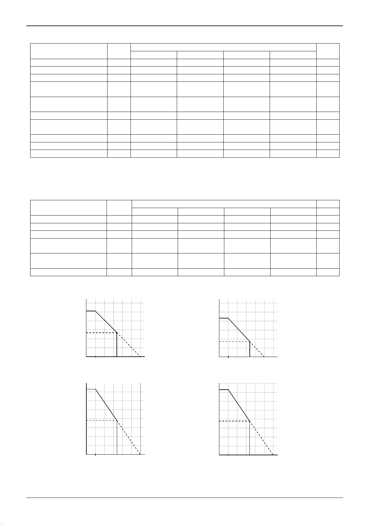
●Power Dissipation Reduction
510
430
265
172
Power Dissipation:Pd[mW]
0 25 85 150
Ambient Temperature:Ta[ ° C]
Fig.1 BD6883GUL Power Dissipation Reduction Fig.2 BH6453GUL Power Dissipation Reduction
730
Power Dissipation:Pd[mW]
0
25 85
Ambient Temperature:Ta[ ° C ]
730
125
380
380
Power Dissipation:Pd[mW]
0
25
Ambient Temperature:Ta[ ° C]
Fig.3 BD6886GUL Power Dissipation Reduction Fig.4 BD6369GUL Power Dissipation Reduction
85 150
Power Dissipation:Pd[mW]
0 25 85 150
Ambient Temperature:Ta[ ° C]
www.rohm.com
© 2012 ROHM Co., Ltd. All rights reserved.
2/16
2012.03 - Rev.
Page 3
BD6883GUL,BH6453GUL,BD6886GUL,BD6369GUL
A
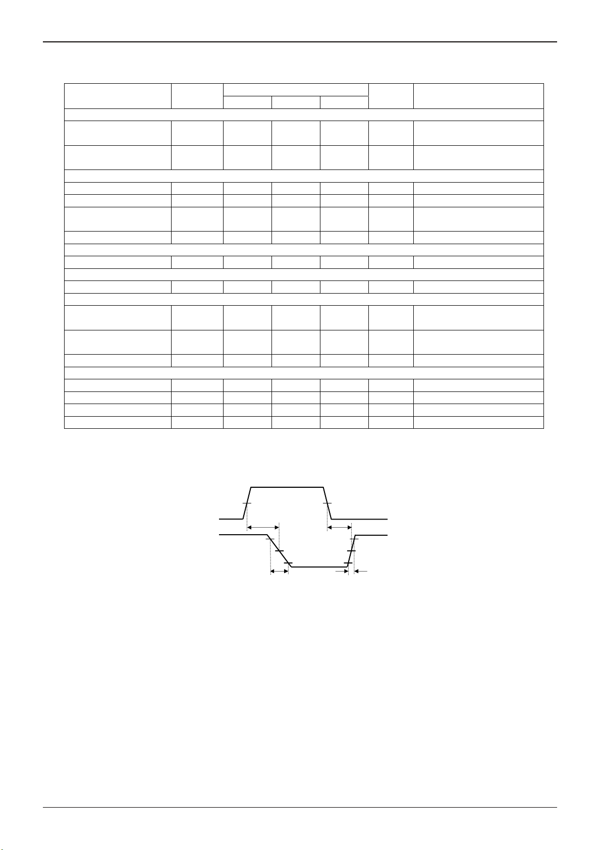
●Electrical Characteristics
1) BD6883GUL Electrical Characteristics (Unless otherwise specified, Ta=25°C, VCC=3.0V)
Parameter Symbol
Overall
Circuit current
during standby operation
Circuit current ICC - 0.9 1.4 mA
Control input (VIN=IN, PS)
High level input voltage VINH 2.0 - VCC V
Low level input voltage VINL 0 - 0.7 V
High level input current IINH 15 30 60 μA
Low level input current IINL -1 0 - μA VINL=0V
Input for Constant-Voltage setting
Input current IVLIM -1.5 -0.5 - μA VLIM=0V
UVLO
UVLO voltage VUVLO 1.6 - 2.4 V
Constant-Voltage Drive block
PMOS Output
ON-Resistance
NMOS Output
ON-Resistance
Output high-level voltage VOH 1.9×VLIM 2.0×VLIM 2.1×VLIM V VLIM=1V with 10Ω load
Output AC characteristic
Turn-on time ton - 1.5 5 μs Io=-150mA, 10Ω load
Turn-off time toff - 0.1 2 μs Io=-150mA, 10Ω load
Rise time tr - 1.5 8 μs Io=-150mA, 10Ω load
Fall time tf - 0.05 1 μs Io=-150mA, 10Ω load
ICCST - 0 10 μA PS=0V
RONP - 0.65 0.80 Ω Io=-150mA
RONN - 0.40 0.60 Ω Io=+150mA
Min Typ Max
Limit
Unit Conditions
PS=3V, VLIM=3V
with no signal and load
VINH=3V,
pull-down resistor typ.100kΩ
VIN
Motor current
50% 50%
ton toff
-10%
-50% -50%
tr tf
-10%
-90% -90%
100%
0%
0%
-100%
Fig.5 BD6883GUL I/O Switching Waveform
(The direction flowing into IC is plus)
Technical Note
www.rohm.com
© 2012 ROHM Co., Ltd. All rights reserved.
3/16
2012.03 - Rev.
Page 4
BD6883GUL,BH6453GUL,BD6886GUL,BD6369GUL
A
2) BH6453GUL Electrical Characteristics (Unless otherwise specified, Ta=25°C, VCC=3.0V)
Parameter Symbol
Overall
Circuit current
during standby operation
Circuit current ICC - 0.9 1.3 mA PS=3V, IN=3V, no load
Control input (VIN=IN, PS)
High-level input voltage VINH 1.5 - VCC V
Low-level input voltage VINL 0 - 0.5 V
High-level input current IINH 15 30 60 μA
Low-level input current IINL -1 0 - μA VINL=0V
UVLO
UVLO voltage VUVLO 1.6 - 2.2 V
Constant-Current Drive block
PMOS Output
ON-Resistance
NMOS Output
ON-Resistance
Offset current Iofs 0 1 5 mA CLIM=0V
Output current Iout 180 200 220 mA CLIM=0.8V, RL=10Ω
ICCST - 0 5 μA PS=0V
RONP - 1.2 1.5 Ω Io=-200mA
RONN - 0.35 0.50 Ω Io=+200mA
Min Typ Max
Limit
Unit Conditions
Drive system of Constant-Current
I
SINK
CLIM[V]
[A]=
2×2.0(Typ.)[Ω]
: VCC-OUT current
I
SINK
CLIM: VCC-OUT current setting voltage
: VCC-OUT current detection resistance
R
RNF
Technical Note
VINH=3V,
pull down resistance typ.100kΩ
www.rohm.com
© 2012 ROHM Co., Ltd. All rights reserved.
4/16
2012.03 - Rev.
Page 5
BD6883GUL,BH6453GUL,BD6886GUL,BD6369GUL
A
Technical Note
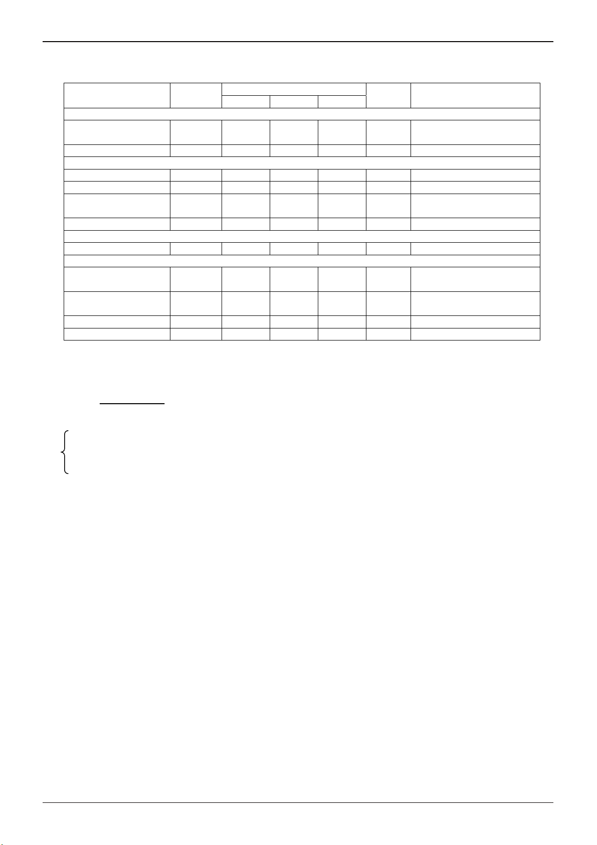
3) BD6886GUL, BD6369GUL Electrical Characteristics (Unless otherwise specified, Ta=25°C, VCC=3.0V, VM=5.0V)
Parameter Symbol
Min Typ Max
Overall
Circuit current
during standby operation
ICCST - 0 10 μA PS=0V
Circuit current 1 ICC - 0.9 1.4 mA PS=3V, with no signal
Circuit current 2 IM - 0.4 0.65 mA PS=3V, VLIM=5V, no load
Control input (VIN=INA, INB, SEL, PS)
High-level input voltage VINH 2.0 - VCC V
Low-level input voltage VINL 0 - 0.7 V
High-level input current IINH 15 30 60 μA VINH=3V
Low-level input current IINL -1 0 - μA VINL=0V
Pull-down resistor RIN 50 100 200 kΩ
Input for Constant-Voltage setting
Input current IVLIM -1.5 -0.5 - μA VLIM=0V
UVLO
UVLO voltage VUVLO 1.6 - 2.4 V
Constant-Voltage Drive block
Output ON-Resistance RON - 0.80 1.20 Ω
Output high-level voltage VOH 1.9×VLIM 2.0×VLIM 2.1×VLIM V VLIM=1V with 10Ω load
Output AC characteristic
Turn-on time ton - 1.5 5 μs Io=±150mA with 10Ω load
Turn-off time toff - 0.1 2 μs Io=±150mA with 10Ω load
Rise time tr - 2 8 μs Io=±150mA with 10Ω load
Fall time tf - 0.05 1 μs Io=±150mA with 10Ω load
Limit
Unit Conditions
Io= ± 150mA on high and low
sides in total
VIN
Motor current
50% 50%
ton
toff
90%
50% 50%
10%
-10%
-50% -50%
tf tr tf tr
ton
toff
10%
-10%
-90% -90%
90%
100%
0%
100%
0%
-100%
Fig.6 BD6886GUL, BD6369GUL I/O Switching Waveform
www.rohm.com
© 2012 ROHM Co., Ltd. All rights reserved.
5/16
2012.03 - Rev.
Page 6
BD6883GUL,BH6453GUL,BD6886GUL,BD6369GUL
A
(
L
)
(
L
)
(
(
(
(
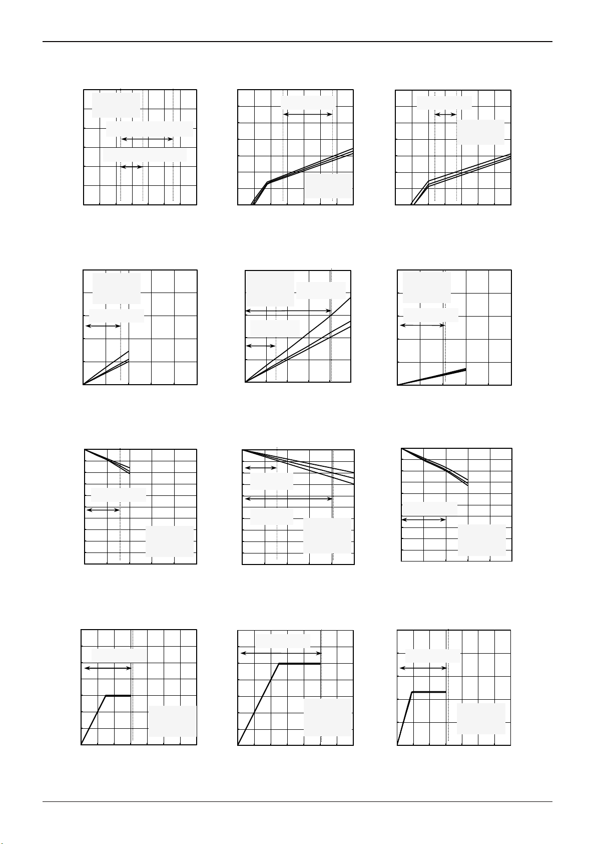
●Electrical Characteristic Diagrams
10.0
Top 85 ℃
Middle 25℃
8.0
A]
μ
6.0
4.0
2.0
Standby current, Icc [
0.0
-2.0
Lower -2
Op. range (2.5V~5.5V)
(BD6883GUL, BD6886GUL,
Op. range (2.3V~3.6 V)
(BH6453GUL)
0.0 1.0 2.0 3.0 4.0 5.0 6.0 7.0
Supply voltage, Vcc [V]
Fig.7 Standby Current
(All series)
BD6883GUL
Output voltage, VOUTL [V]
0.5
0.4
0.3
0.2
0.1
Top 85 ℃
Middle 25℃
Lower -2
5℃VM=VC
Op. range (0~150mA)
All series
BD6883GUL / BD6886GUL / BD6369GUL
3.5
3.0
2.5
2.0
1.5
Circuit current, Icc [mA]
1.0
0.5
0.0
0.0 1.0 2.0 3.0 4.0 5.0 6.0 7.0
Op. range (2.5V~5.5V)
Supply voltage, Vcc [V]
Middle 25℃
Fig.8 Circuit Current
(BD6883GUL/BD6886GUL/BD6369GUL)
BD6886GUL / BD6369GUL
Output voltage, VOUTL [V]
0.5
0.4
0.3
0.2
0.1
Top 85 ℃
Middle 25℃
Lower -2
5℃
=
Op. range (0~150mA)
(BD6886GUL)
Op. range (0~400mA)
(BD6369GUL)
Top 85 ℃
Lower -2
Technical Note
5℃Lower -
BH6453GUL
BH6453GUL
Top 85 ℃
Middle 2
3.5
3.0
2.5
2.0
1.5
Circuit current, Icc [mA]
1.0
0.5
0.0
Op. range (2.3V~3.6V)
0.01.02.03.04.05.06.07.0
Supply voltage, Vcc [V]
Fig.9 Circuit Current
(BH6453GUL)
Output voltage, VOUTL [V]
5.0
4.0
3.0
2.0
1.0
Top 85 ℃
Middle 25℃
Lower -2
5℃VM=VC
Op. range (0~200mA)
0.0
0 0.1 0.2 0.3 0.4 0.5
Output current, Io [A]
Fig.10 NMOS Output Voltage
BD6883GUL)
BD6883GUL
Top -25℃
Middle 25℃
Lower 85℃
VM=VCC=3
0.0
-0.1
-0.2
-0.3
Op. range (0~150mA)
-0.4
-0.5
-0.6
-0.7
Output voltage, VOUTH [V]
-0.8
-0.9
-1.0
0 0.1 0.2 0.3 0.4 0.5
Output current, Io [A]
Fig.13 PMOS Output Voltage
(BD6883GUL)
BD6883GUL
Top -25℃
Middle 25℃
Lower 85℃
VM=VCC=3
7.0
6.0
Op. range (0~VCC)
5.0
4.0
3.0
OUT voltage, VOH [V]
2.0
1.0
0.0
0.0 1.0 2.0 3.0 4.0 5.0 6.0 7.0
VLIM voltage [V]
Fig.16 Output High-Level Voltage
BD6883GUL)
0.0
0 0.1 0.2 0.3 0.4 0.5
Output current, Io [A]
Fig.11 NMOS Output Voltage
(BD6886GUL / BD6369GUL)
BD6886GUL / BD6369GUL
Op. range
(0~150mA)
BD6886GU
Op. range
(0~400mA)
BD6369GU
0 0.1 0.2 0.3 0.4 0.5
Output current, Io [A]
Top 85 ℃
Middle 25℃
Lower -2
5℃
=
Output voltage, VOUTH [V]
0.0
-0.1
-0.2
-0.3
-0.4
-0.5
-0.6
-0.7
-0.8
-0.9
-1.0
Fig.14 PMOS Output Voltage
(BD6886GUL / BD6369GUL)
7.0
6.0
5.0
4.0
3.0
OUT voltage, VOH [V]
2.0
1.0
0.0
0.0 1.0 2.0 3.0 4.0 5.0 6.0 7.0
BD6886GUL / BD6369GUL
Op. range (0~VM)
Top -25℃
Middle 25℃
Lower 85℃
VM=5V
VCC=3V
VLIM voltage [V]
Fig.17 Output High-Level Voltage
(BD6886GUL / BD6369GUL)
0.0
0 0.1 0.2 0.3 0.4 0.5
Output current, Io [A]
Fig.12 NMOS Output Voltage
BH6453GUL)
0.0
-0.1
-0.2
-0.3
-0.4
-0.5
Op. range (0~200mA)
-0.6
-0.7
Output voltage, VOUTH [V]
-0.8
-0.9
-1.0
0 0.1 0.2 0.3 0.4 0.5
BH6453GUL
Middle 25℃
Lower 85℃
VM=VCC=3
Output current, Io [A]
Top -25℃
Fig.15 PMOS Output Voltage
BH6453GUL
500
Op. range (0~VCC)
400
300
200
Top -25℃
Middle 25℃
Lower 85℃
VM=VCC=3
OUT current, IOUT [mA]
100
0
0.01.02.03.04.05.06.07.0
CLIM voltage, VCLIM [V]
Fig.18 Current Limit Output Voltage
BH6453GUL)
www.rohm.com
© 2012 ROHM Co., Ltd. All rights reserved.
6/16
2012.03 - Rev.
Page 7

BD6883GUL,BH6453GUL,BD6886GUL,BD6369GUL
A
● Block Diagram, Application Circuit Diagram, Pin Arrangement, Pin Function Table
1) BD6883GUL Block Diagram, Application Circuit Diagram, Pin Arrangement, Pin Function Table
Bypass filter Capacitor for power
supply input. See. P.14/16.
Setting for Constant-Voltage input terminal
In addition to the DC input, PW M signal drive
is also possible using filter com ponents.
See. P.11/16
Power-Saving
H: Active
L: Standby
Motor control input
PS
VLIM
0.1~10uF
1A
Power Save
IN
2A
Logic
2B
1B
TSD & UVLO
Pre Driver
VCC
BandGap
×2
VCC
I
SOURCE
1C
OUT
GND
2C
Fig.19 BD6883GUL Block Diagram, Application Circuit Diagram
1 2
Technical Note
0.5ch Constant-Voltage output pins.
Output H voltage.
OUT[V]=2×VLIM[V]
A
PS IN
B
VCC VLIM
C OUT GND
Fig.20 BD6883GUL Pin Arrangement (Top View)
BD6883GUL Pin Function Table
No.
Pin
Name
Function No.
Pin
Name
Function
1A PS Power-saving pin 2B VLIM Output high-level voltage setting pin
2A IN Control input pin 1C OUT Half-bridge output pin
1B VCC Power supply pin 2C GND Ground pin
www.rohm.com
© 2012 ROHM Co., Ltd. All rights reserved.
7/16
2012.03 - Rev.
Page 8

BD6883GUL,BH6453GUL,BD6886GUL,BD6369GUL
A
2) BH6453GUL Block Diagram, Application Circuit Diagram, Pin Arrangement, Pin Function Table
Bypass filter Capacitor for power
supply input. See. P.14/16.
Power-Saving
H: Active
L: Standby
PS
B1
Power Save
Motor control input
IN
A1
CLIM
A2
Logic
0.1~10uF
TSD & UVLO
Pre Driver
V/I converter
VCC
BandGap
VCC
OUT
RNF=2.0Ω
Setting for Constant-Current input term inal
In addition to the DC input, PW M signal drive
is also possible using filter com ponents.
See. P.11/16
GND
Fig.21 BH6453GUL Block Diagram, Application Circuit Diagram
1 2 3
A
IN CLIM GND
0.5ch Constant-Current output pins.
IOUT[mA] = CLIM[V] / (2×2(Typ)[Ω])
I
SINK
VCC
Technical Note
PS VCC OUT
B
Fig.22 BH6453GUL Pin Arrangement (Top View)
BH6453GUL Pin Function Table
No.
Pin
Name
Function No.
Pin
Name
1A IN Control input pin 1B PS Power-saving pin
2A CLIM Output current setting pin 2B VCC Power supply pin
3A GND Ground pin 3B OUT Half-bridge output pin
Function
www.rohm.com
© 2012 ROHM Co., Ltd. All rights reserved.
8/16
2012.03 - Rev.
Page 9

BD6883GUL,BH6453GUL,BD6886GUL,BD6369GUL
A
3) BD6886GUL, BD6369GUL Block Diagram, Application Circuit Diagram, Pin Arrangement, Pin Function Table
Bypass filter Capacitor for power
supply input. See. P.14/16.
Control Input mode selection
Setting for Constant-Voltage input terminal
In addition to the DC input, PW M signal drive
possible using filter components.
is also
See. P.11/16
Power-Saving
H: Active
L: Standby
Motor control input
INA
INB
SEL
VLIM
PS
3A
4B
3B
3C
2C
Power Save
Logic
0.1~10uF
4C
TSD & UVLO
Pre Driver
3D
VCC
BandGap
H bridge
×2
GND
Bypass filter Capacitor for power
supply input. See. P.14/16.
0.1~10uF
1B
VM
2A
OUTA
OUTB
2D
PGND
1C
I
OUT
1ch Constant-Voltage output pins.
Output H voltage.
OUT[V]=2×VLIM[V]
Fig.23 BD6886GUL, BD6369GUL Block Diagram, Application Circuit Diagram
1 2 3 4
A
N.C. OUTA PS N.C.
Technical Note
B
VM
INDEX
POST
INB INA
PGND VLIM SEL VCC
C
D
N.C. OUTB GND N.C.
Fig.24 BD6886GUL, BD6369GUL Pin Arrangement (Top View)
BD6886GUL, BD6369GUL Pin Function Table
No.
Pin
Name
Function No.
Pin
Name
Function
1A N.C. N.C. 1C PGND Motor ground pin
2A OUTA H-bridge output pin A 2C VLIM Output high-level voltage setting pin
3A PS Power-saving pin 3C SEL Control input mode selection pin
4A N.C. N.C. 4C VCC Power supply pin
1B VM Motor power supply pin 1D N.C. N.C.
2B 2D OUTB H-bridge output pin B
3B INB Control input pin B 3D GND Ground pin
4B INA Control input pin A 4D N.C. N.C.
www.rohm.com
© 2012 ROHM Co., Ltd. All rights reserved.
9/16
2012.03 - Rev.
Page 10

BD6883GUL,BH6453GUL,BD6886GUL,BD6369GUL
A
●Function Explanation
1) Power-saving function (all series)
When the L voltage is applied the PS pin, the IC’s inside circuit stop, and when 0V applied, the circuit current became
0μA(Typ.), especially.
When the IC drive, serial input while the PS pin applied H voltage. (See the electrical characteristics; P.3, 4, 5/16)
2) Control Input Pin
(Ⅰ)IN pin (BD6883GUL, BH6453GUL)
The IN pin is used to program and control the motor drive modes.
(See the electrical characteristics; P3, 4/16, and the I/O Truth Table; P12/16)
(Ⅱ)INA, INB, SEL pins (BD6886GUL, BD6369GUL)
The INA and INB are used to program and control the motor drive modes.
When the L voltage is applied to the SEL pin, the I/O logic can be set to EN (Enable)/IN mode, and when the H voltage is applied
to the one, the I/O logic can be set to IN/IN mode. (See the electrical characteristics; P5/16, and the I/O Truth Table; P12/16)
3) H-bridge and Half-bridge on the output stage (ALL series)
Specify maximum current applied to the H-bridge and Half-bridge within the operating range, in consideration of power dissipation.
(See the Operating Conditions; P.2/16)
4) Drive system of Linear Constant-Voltage H-bridge (BD6883GUL, BD6886GUL, and BD6369GUL)
To set up the output H voltage, when the voltage input to the VLIM pin, the output H voltage is two times as high as the voltage.
(Ⅰ)BD6883GUL
The output H voltage VOH [V] = 2.0×VLIM [V] (When VLIM [V] > , Output H voltage is about VCC voltage)
(Ⅱ)BD6886GUL, BD6369GUL
The output H voltage VOH [V] = 2.0×VLIM [V] (When VLIM [V] > , Output H voltage is about VM voltage)
For example, the output voltage is 2.0V±5%, if 1.0V is applied to the VLIM pin.
If the VLIM pin is shorted to the VM pin (or the same voltage level as the VM is applied), you can be used as a Full-ON Drive
H-bridge.
VCC [V]
2
VM [V]
2
5) Drive system of Linear Constant-Current H-bridge (BH6453GUL)
To detect the output current and the output current settings
The BH6453GUL built in resistor for output current detect. The output current is kept constant by comparing it with the CLIM
voltage. In addition, impress a highly accurate voltage form the outside of IC to the CLIM terminal, when you do the output current
setting accuracy or more good.
Output current I
SINK
[A] =
CLIM [V]
2×2(Typ) [Ω]
If the CLIM pin applied 0.8V, Output current is 200mA±10%.
Technical Note
・・・・・①
・・・・・②
・・・・・③
www.rohm.com
© 2012 ROHM Co., Ltd. All rights reserved.
10/16
2012.03 - Rev.
Page 11

BD6883GUL,BH6453GUL,BD6886GUL,BD6369GUL
A
7) Setting of PWM signal input VLIM and CLIM terminals (all series)
It is also possible to compose filters outside the IC, change an input voltage for output voltage and output current setting terminals
such as VLIM and CLIM terminals by the DUTY control using an PWM signal, etc., and use them as set values for control.
In this case, however, ensure the smoothing of the signals, heeding the constant number of the low-pass filter as stated below.
A cutoff frequency F
Cutoff frequency F
Set the cutoff frequency F
For example, if the cutoff frequency F
above:
Cutoff frequency F
When C
=0.1[μF], according to the formula above:
IN
R
INA
Where, an effective value of PWM signal as a DC current, according to crest values V
is as follows:
V
PWM
An actual voltage V
is as follows according to resistance potential division of R
V
LIM
For example, when an PWM signal with crest values V
above is:
V
LIM
(Ⅰ)BD6883GUL, BD6886GUL, and BD6369GUL
Where, to specify an output voltage VOH=2[V], a value VLIM=1.0[V] according to the formula in the previous page. And then,
according to the formula above, VLIM=1.0[V].
VLIM=1.0[V]=V
Therefore, R
INA
⑩
According to ⑥ and ⑩, R
(Ⅱ)BH6453GUL
Where, to specify an output current I
③, CLIM=0.4[V], and according to the formula above ⑨:
CLIM=0.4[V]=V
R
INA
According to ⑥ and ⑪: R
V
MAX
V
PWM
(-3dB attenuation frequency) of the low-pass filter in Fig25 is calculated by the formula mentioned below.
C
[Hz] = [Hz]
C
at 1/100 or below of the PWM frequency F
C
[Hz] =
C
//R
=3.2[kΩ]
INB
[V]= V
[V]= ×V
[V]= × 3[V]× 50[%]
=0.5R
=2.75R
[V]× ON DUTY[%]
MAX
input to terminals that specify output current and voltages, such as VLIM and CLIM terminals
LIM
R
INB
R
R
INB
INB
INA+RINB
R
INB
INA+RINB
R
INB
= ×3[V]×50[%]
LIM
R
INA+RINB
・・・・・
=4.8kΩ, R
INA
SINK
R
= ×3[V]×50[%]
LIM
F
PWM
INB
R
INA+RINB
=11.9kΩ, R
INA
1
2πC
(R
//R
INA
INB
)
when the PWM frequency F
PWM
IN
is set at 1/100 of F
C
1
2πC
(R
//R
)
INA
INB
=3[V] and DUTY [%]=5[%] is input, a V
MAX
PWM
IN
[V]
=9.6kΩ.
INB
=100[mA], the following formula is derived according to the formula in the previous page
=4.3kΩ
INB
R
INA
V
R
INB
Fig.25 Example PWM signal input
Technical Note
.
PWM
=50[kHz], according to the formula
PWM
1
= ×F
100
and R
INA
Output voltage / Constant current voltage terminals
LIM
VLIM / CLIM
CIN
50×103
= [Hz]
PWM
100
and ON DUTY [%]=
MAX
:
INB
value according to the formula
LIM
・・・・・④
・・・・・⑤
・・・・・⑥
ON time
ON time+ OFF time
・・・・・⑦
・・・・・⑧
・・・・・⑨
・・・・・⑪
www.rohm.com
© 2012 ROHM Co., Ltd. All rights reserved.
11/16
2012.03 - Rev.
Page 12

BD6883GUL,BH6453GUL,BD6886GUL,BD6369GUL
A
●I/O Truth Table
BD6883GUL I/O Truth Table
MODE
- H
- L X Z
L: Low, H: High, X: Don’t care, Z: Hi impedance
Sink is a direction of current flowing into the driver, and Source is a direction of current flowing out the driver.
When it is sink, which drive FULL ON.
7
※
Z at the Constant-Voltage driver output L voltage for connect feedback resistance (20kΩ Typ.) for output H voltage setting between OUT pin and GND.
But output Power MOS is OFF condition.
INPUT OUTPUT
PS IN OUT
OUTPUT MODE
L L Sink
H H Source
7
※
Standby
BH6453GUL I/O Truth Table
MODE
- H
INPUT OUTPUT
PS IN OUT
OUTPUT MODE
H L Sink
L H Source
- L X Z Standby
L: Low, H: High, X: Don’t care, Z: Hi impedance
Sink is a direction of current flowing into the driver, and Source is a direction of current flowing out the driver.
When it is source, which drive FULL ON.
BD6886GUL, BD6369GUL I/O Truth Table
MODE
EN/IN
PS SEL INA INB OUTA OUTB
INPUT OUTPUT
L X Z
L
H L H L Forward rotation
※
H H L H Reverse rotation
H
IN/IN H
- L X X X Z
L: Low, H: High, X: Don’t care, Z: Hi impedance
At forward rotation, current flows from OUTA to OUTB. At reverse rotation, current flows from OUTB to OUTA.
8
※
Z at the Constant-Voltage driver output L voltage for connect feedback resistance (20kΩ Typ.) for output H voltage setting between OUT pin and GND.
But output Power MOS is OFF condition.
L L L L Brake
L H L H Reverse rotation
H L H L Forward rotation
H H Z
※
※
7
Z
8
Z
8
Z
7
※
Standby
8
※
Standby
8
※
Standby
Technical Note
OUTPUT MODE
www.rohm.com
© 2012 ROHM Co., Ltd. All rights reserved.
12/16
2012.03 - Rev.
Page 13

BD6883GUL,BH6453GUL,BD6886GUL,BD6369GUL
A
k
k
A
●I/O Circuit Diagram
PS, IN OUT, GND
VCC
VCC
PS
IN
10k
OUT
100k
GND
Fig.26 BD6883GUL I/O Circuit Diagram (Resistance values are typical ones.)
PS
PS
25k
VCC
140
75k
IN
IN
VCC
10k
100k
CLIM
VCC
CLIM
1k
Fig.27 BH6453GUL I/O Circuit Diagram (Resistance values are typical ones.)
PS, INA, INB, SEL VM, OUTA, OUTB, PGND
PS
INA
INB
SEL
VCC
10k
100k
OUT
Fig.28 BD6886GUL, BD6369GUL I/O Circuit Diagram (Resistance values are typical ones.)
140
VM
OUTB
PGND
60k
VLIM
VLIM
OUT, GND
VLIM
VLIM
Technical Note
VCC
1k
10k
VCC
OUT
GND
VCC
1k
10k
www.rohm.com
© 2012 ROHM Co., Ltd. All rights reserved.
13/16
2012.03 - Rev.
Page 14

BD6883GUL,BH6453GUL,BD6886GUL,BD6369GUL
A
●Operation Notes
1) Absolute maximum ratings
Use of the IC in excess of absolute maximum ratings, such as the applied voltage (VCC, VM) or operating temperature
range (Topr), may result in IC damage. Assumptions should not be made regarding the state of the IC (short mode or
open mode) when such damage is suffered. A physical safety measure, such as a fuse, should be implemented when
using the IC at times where the absolute maximum ratings may be exceeded.
2) Storage temperature range (Tstg)
As long as the IC is kept within this range, there should be no problems in the IC’s performance. Conversely, extreme
temperature changes may result in poor IC performance, even if the changes are within the above range.
3) Power supply and wiring
Be sure to connect the power terminals outside the IC. Do not leave them open. Because a return current is
generated by a counter electromotive force of the motor, take necessary measures such as putting a Capacitor
between the power source and the ground as a passageway for the regenerative current. Be sure to connect a
Capacitor of proper capacitance (0.1μF to 10μF) between the power source and the ground at the foot of the IC, and
ensure that there is no problem in properties of electrolytic Capacitors such as decrease in capacitance at low
temperatures. When the connected power source does not have enough current absorbing capability, there is a
possibility that the voltage of the power source line increases by the regenerative current an exceeds the absolute
maximum rating of this product and the peripheral circuits.
Therefore, be sure to take physical safety measures such as putting a zener diode for a voltage clamp between the
power source an the ground.
4) Ground terminal and wiring
The potential at GND terminals should be made the lowest under any operating conditions. Ensure that there are no
terminals where the potentials are below the potential at GND terminals, including the transient phenomena. The
motor ground terminals PGND, and the small signal ground terminal GND are not interconnected with one another
inside the IC. It is recommended that you should isolate the large-current RNF pattern and PGND pattern from the
small-signal GND pattern, and should establish a one-point grounding at a reference point of the set, to avoid
fluctuation of small-signal GND voltages caused by voltage changes due to pattern wire resistances and large
currents. Also prevent the voltage variation of the ground wiring patterns of external components. Use short and thick
power source and ground wirings to ensure low impedance.
5) Thermal design
Use a proper thermal design that allows for a sufficient margin of the power dissipation (Pd) at actual operating
conditions.
6) Pin short and wrong direction assembly of the device.
Use caution when positioning the IC for mounting on printed circuit boards. The IC may be damaged if there is any
connection error or if positive and ground power supply terminals are reversed. The IC may also be damaged if pins
are shorted together or are shorted to other circuit’s power lines.
7) Avoiding strong magnetic field
Malfunction may occur if the IC is used around a strong magnetic field.
8) ASO
Ensure that the output transistors of the motor driver are not driven under excess conditions of the absolute maximum
ratings and ASO.
9) TSD (Thermal Shut Down) circuit
If the junction temperature (Tjmax) reaches 175°C (but the BH6453GUL is 150°C), the TSD circuit will operate, and
the coil output circuit of the motor will open. There is a temperature hysterics of approximately 25°C (but the
BH6453GUL is 20°C). The TSD circuit is designed only to shut off the IC in order to prevent runaway thermal
operation. It is not designed to protect the IC or guarantee its operation. The performance of the IC’s characteristics is
not guaranteed and it is recommended that the device is replaced after the TSD is activated.
Technical Note
www.rohm.com
© 2012 ROHM Co., Ltd. All rights reserved.
14/16
2012.03 - Rev.
Page 15

BD6883GUL,BH6453GUL,BD6886GUL,BD6369GUL
A
10) Testing an application board
When testing the IC on an application board, connecting a Capacitor to a pin with low impedance subjects the IC to
stress. Always discharge Capacitors after each process or step. Always turn the IC's power supply off before
connecting it to, or removing it from a jig or fixture, during the inspection process. Ground the IC during assembly
steps as an antistatic measure. Use similar precaution when transporting and storing the IC.
11) Regarding the input pin of the IC
This monolithic IC contains P
+
isolation and P substrate layers between adjacent elements to keep them isolated. P-N
junctions are formed at the intersection of these P layers with the N layers of other elements, creating a parasitic
diode or transistor. For example, the relation between each potential is as follows:
When GND > Pin A, the P-N junction operates as a parasitic diode.
When GND > Pin B, the P-N junction operates as a parasitic diode and transistor.
Parasitic elements can occur inevitably in the structure of the IC. The operation of parasitic elements can result in
mutual interference among circuits, operational faults, or physical damage. Accordingly, methods by which parasitic
elements operate, such as applying a voltage that is lower than the GND (P substrate) voltage to an input pin, should
not be used.
Pin A
Parasitic element
N
P+ P
P
GND
Resistor Transistor (NPN)
Pin B
Pin A
N
+
N N
P substrate
Parasitic
element
P+
Parasitic elements
Technical Note
B
C
N
E
P
P substrate
GND
P+
N
GND
Pin B
B C
E
Parasitic
GND
elements
Other adjacent elements
Fig.29 Example of Simple IC Architecture
www.rohm.com
© 2012 ROHM Co., Ltd. All rights reserved.
15/16
2012.03 - Rev.
Page 16

BD6883GUL,BH6453GUL,BD6886GUL,BD6369GUL
A
(
(
(
●Selecting a Model Name when Ordering
Technical Note
B X 6 X X X
Rohm model name
6883 : Constant voltage 0.5ch
6453 : Constant current 0.5ch
6886 : Constant voltage 1ch
6369 : Constant voltage 1ch
VCSP50L1 (BD6883GUL)
< Dimension >
G U L
E 2
Package
GUL : VCSP50L1 (BD6883)
GUL : VCSP50L1 (BH6453)
GUL : VCSP50L2 (BD6886)
GUL : VCSP50L2 (BD6369)
< Tape and Reel information >
Tape
Quantity
Direction
of feed
Embossed carrier tape (with dry pack)
3000pcs
E2
(The direction is the 1pin of product is at the upper left when you hold
reel on the left hand and you pull out the tape on the right hand.)
1234 1234 1234 1234 1234 1234
Packaging and forming specification
E2: Embossed tape and reel
Unit:mm)
VCSP50L1 (BH6453GUL)
<
< Dimension >
Tape and Reel information >
Tape
Quantity
Direction
of feed
Unit:mm)
VCSP50L2 (BD6886GUL, BD6369GUL)
<
< Dimension >
Tape and Reel information >
Tape
Quantity
Direction
of feed
Reel
※When you order , please order in times the amount of package quantity.
1Pin
Direction of feed
Embossed carrier tape (with dry pack)
3000pcs
E2
(The direction is the 1pin of product is at the upper left when you hold
reel on the left hand and you pull out the tape on the right hand.)
1234 1234 1234 1234 1234 1234
Unit:mm)
www.rohm.com
© 2012 ROHM Co., Ltd. All rights reserved.
Reel
※When you order , please order in times the amount of package quantity.
16/16
1Pin
Direction of feed
2012.03 - Rev.
Page 17

Notes
No copying or reproduction of this document, in part or in whole, is permitted without the
consent of ROHM Co.,Ltd.
The content specied herein is subject to change for improvement without notice.
The content specied herein is for the purpose of introducing ROHM's products (hereinafter
"Products"). If you wish to use any such Product, please be sure to refer to the specications,
which can be obtained from ROHM upon request.
Examples of application circuits, circuit constants and any other information contained herein
illustrate the standard usage and operations of the Products. The peripheral conditions must
be taken into account when designing circuits for mass production.
Great care was taken in ensuring the accuracy of the information specied in this document.
However, should you incur any damage arising from any inaccuracy or misprint of such
information, ROHM shall bear no responsibility for such damage.
The technical information specied herein is intended only to show the typical functions of and
examples of application circuits for the Products. ROHM does not grant you, explicitly or
implicitly, any license to use or exercise intellectual property or other rights held by ROHM and
other parties. ROHM shall bear no responsibility whatsoever for any dispute arising from the
use of such technical information.
The Products specied in this document are intended to be used with general-use electronic
equipment or devices (such as audio visual equipment, ofce-automation equipment, communication devices, electronic appliances and amusement devices).
The Products specied in this document are not designed to be radiation tolerant.
While ROHM always makes efforts to enhance the quality and reliability of its Products, a
Product may fail or malfunction for a variety of reasons.
Please be sure to implement in your equipment using the Products safety measures to guard
against the possibility of physical injury, re or any other damage caused in the event of the
failure of any Product, such as derating, redundancy, re control and fail-safe designs. ROHM
shall bear no responsibility whatsoever for your use of any Product outside of the prescribed
scope or not in accordance with the instruction manual.
The Products are not designed or manufactured to be used with any equipment, device or
system which requires an extremely high level of reliability the failure or malfunction of which
may result in a direct threat to human life or create a risk of human injury (such as a medical
instrument, transportation equipment, aerospace machinery, nuclear-reactor controller, fuelcontroller or other safety device). ROHM shall bear no responsibility in any way for use of any
of the Products for the above special purposes. If a Product is intended to be used for any
such special purpose, please contact a ROHM sales representative before purchasing.
If you intend to export or ship overseas any Product or technology specied herein that may
be controlled under the Foreign Exchange and the Foreign Trade Law, you will be required to
obtain a license or permit under the Law.
Notice
Thank you for your accessing to ROHM product informations.
More detail product informations and catalogs are available, please contact us.
ROHM Customer Support System
www.rohm.com
© 2012 ROHM Co., Ltd. All rights reserved.
http://www.rohm.com/contact/
R1120
A
 Loading...