ROHM BH3810FS Datasheet

1
Multimedia ICs
Vocal fader IC with input selector
BH3810FS
The BH3810FS is a vocal fader IC that is serial control compatible. It has mode switching that also includes a voice
multiplexing mode, a five-input selector, a gain selector and other such features, which can all be controlled serially.
Eight open-collector terminals and two tri-state terminals are provided on the chip to facilitate control by other ICs.
•
Applications
Component stereo systems, CD radio cassette players, TVs and car stereos.
•
Features
•
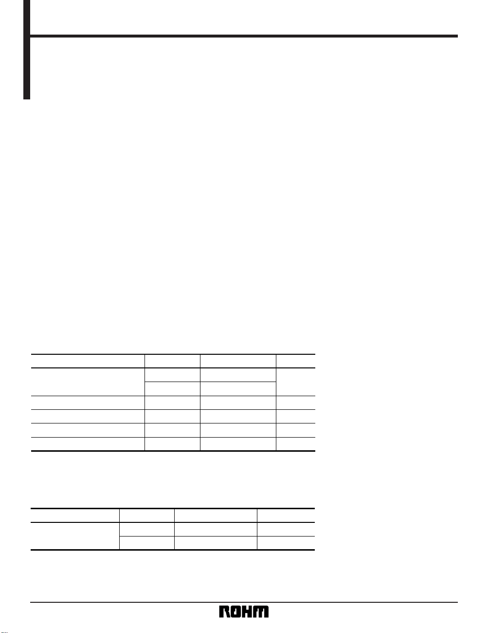
Absolute maximum ratings (Ta = 25°C)
•
Recommended operating conditions (Ta = 25°C)
Parameter
Applied voltages
Power dissipation
Operating temperature
Storage temperature
V
DD
Pd
Topr
Tstg
+ 5.5
850
∗
– 40 ~ + 85
– 55 ~ + 125
V
VEE – 4.5
Symbol Limits Unit
mW
°C
°C
Maximum open collector voltage VOP 14 V
∗
Reduced by 8.5mW for each increase in Ta of 1°C over 25°C ,
when mounted on a 50mm × 50mm × 1.6mm board.
1) Built-in low-pass filter can perform vocal fader function (erasing of vocals from commercially available
music software) using just one chip.
2) Serial control can be used to switch between vocal
fader, through, multiplex, and mute modes.
3) Built-in gain selector allows selection of gain from
6dB to 20dB in 2dB steps.
4) Five-channel input selector.
5) Mic. mixing amplifier with mute function. Key controller input also provided.
6) SSOP-A32 pin package.
Parameter
Power supply voltage
V
DD 4.0 ~ 5.3 V
V
EE – 4.3 ~ – 3.0 V
Symbol Limits Unit

2
Multimedia ICs BH3810FS
•
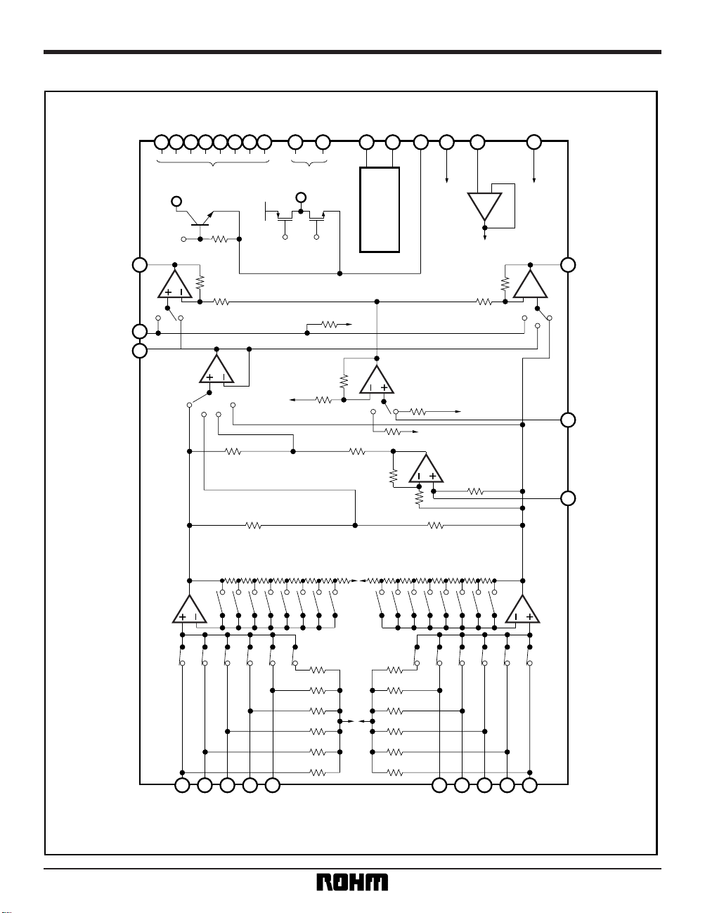
Block diagram
PORT124PORT223PORT322PORT421PORT520PORT619PORT718PORT817PORT916PORT1015SCK14SI13DGND12VDD
11
AGND
10
VEE
VDD
VEE
9
OUTPUT—L
8
MIC
—IN
7
LPF
6
TK
27
FK
26
OUTPUT—R
25
PORT1 ~ 8
7k
50k
50k
50k50k
50k50k
50k
50k
50k
50k
50k
50k
50k
50k
15k
10k
L
R
VF
50k
7k
7k
PORT9 ~ 10
DIGITAL CONTROL
V
DD
+
–
7k
+
–
30k
10k
10k
30k
20k
20k
6dB
(0dB)
8dB
(2dB)
10dB
(4dB)
12dB
(6dB)
14dB
(8dB)
16dB
(10dB)
18dB
(12dB)
20dB
(14dB)
20dB
(14dB)
18dB
(12dB)
16dB
(10dB)
14dB
(8dB)
12dB
(6dB)
10dB
(4dB)
8dB
(2dB)
6dB
(0dB)
—RA
32
—RB
31
—RC
30
—RD
29
INPUT
—RE
28
—LE
5
—LD
4
—LC
3
—LB
2
INPUT
—LA
1

3
Multimedia ICs BH3810FS
•
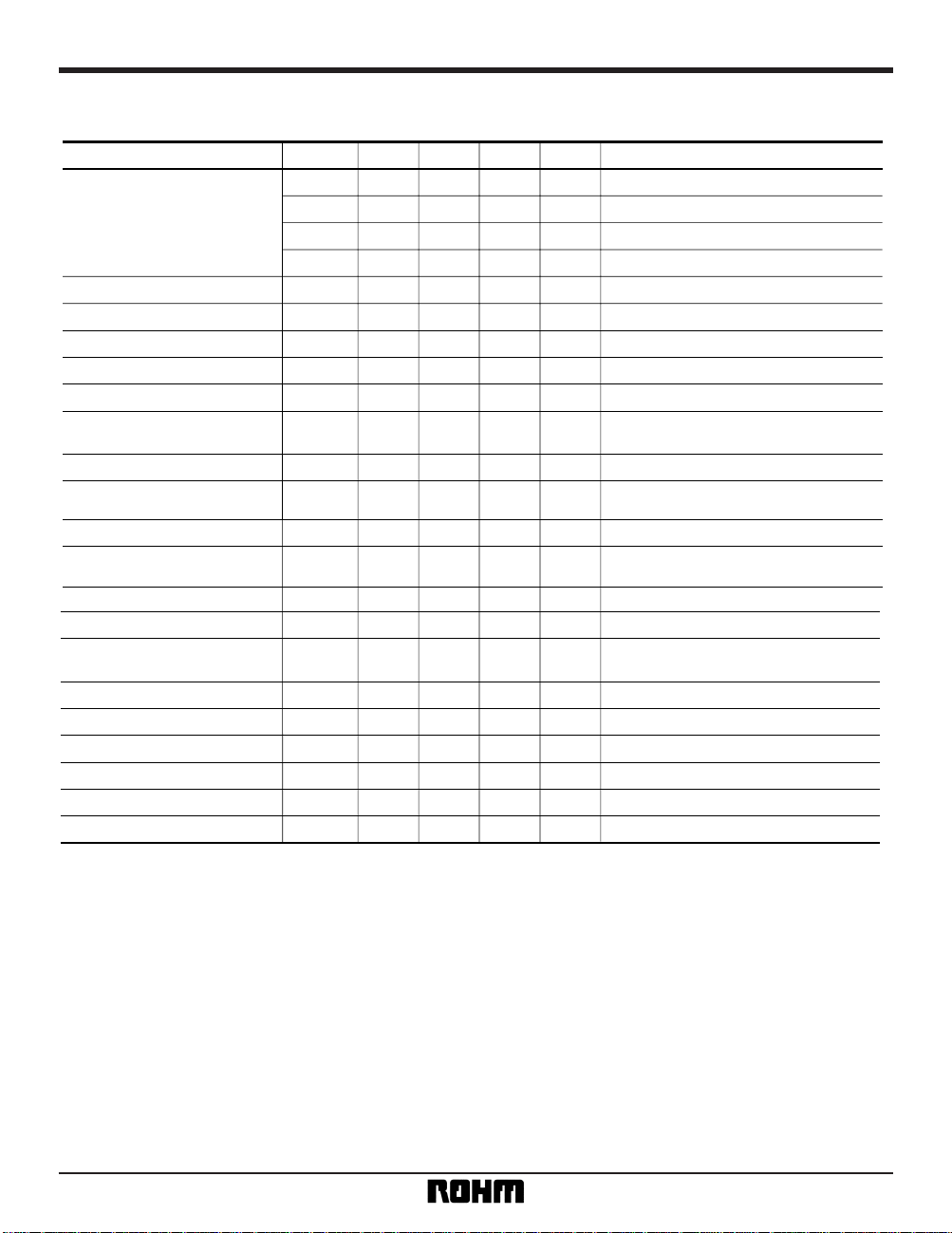
Electrical characteristics (unless otherwise notes, Ta = 25°C, VDD = 5V, VEE = – 4V, G = 14dB, f =1kHz,
Rg = 600Ω, V
IN = 150mV, and RL = 100kΩ)
Parameter
Quiescent current
Maximum output voltage
I
Q1
+
I
Q1
–
I
Q2
+
I
Q2
–
Vom
mA
Symbol
—
—
—
—
1.5
Min.
4.5
4.1
10.0
7.6
2.2
Typ.
10.0
10.0
20.0
20.0
—
V
rms
Max. Unit Conditions
mA
mA
mA
THD
=
1%, through mode
L, R gain
G
VT
11 14 17 dB Through mode
Low-frequency gain
G
VF
8 11 14 dB Vocal fader mode, f
=
100Hz
Microphone gain
G
VM
5 8 11 dB
Crosstalk
CT 54 64
—
dB f
=
1kHz, through mode
f
=
1kHz, mute mode or input mute
Mute attenuation
MU 60 80
—
dB
Vocal suppression ratio
SV 15 20
—
dB Vocal fader mode, f
=
1kHz
Total harmonic distortion
THD
—
0.004 0.05
%
VO =
1V
rms
, through mode, BW 400Hz
to 30kHz
Noise level
V
N
—
15 22
µ
V
rmsRg
=
0, DIN AUDIO
∗
Mode switch output DC
differential
∆
DCB
—
018mV
Between each mode with key controller on
Input impedance
R
IN
35 50 65 k
Ω
Pins 1 to 5, pins 26, pins 28
to
32
Input selector crosstalk
CT
IN
80
——
dB f
=
1kHz
"L" output voltage
V
OL
—
0.15 0.5 V Pins 17
to
27, IOL =
5mA
"H" output leakage current
I
OH
—
0 2.0
µ
A
Pins 17 to 24, 13V applied to collector
Tri-state "H" output voltage
V
SOH
4.5 4.85
—
V Pins 15 to 16, Io
=
1mA
Tri-state "L" output voltage
V
SOL
—
0.05 0.5 V Pins 15 to 16, Io
=
1mA
SI pin source current (pin 13)
I
SI
—
0.4 10
µ
A When SI pin is at DGND potential
SCK pin source current (pin 14)
I
SCK
—
0.2 10
µ
A When SCK pin is at DGND potential
Pins 17 to 24, 0.5V between PORT
terminal and GND voltage = 0.5V
Port output current
I
PMax.
5.0 12
—
mA
Through mode V
EE
current
Through mode V
DD
current
Through mode D9 to D16 data1
Through mode D9 to D16 data1
∗
Measured using a Matsushita VP-9690A (average value detector, effective value display) DIN AUDIO filter.
Operating specifications: same phase for the input and output signals.
䊊 Not designed for radiation resistance.
—
 Loading...