

CMOS LDO Regulator Series for Portable Equipments
Standard CMOS LDO Regulators
BHŜŜ FB1WG series, BHŜŜ FB1WHFV series,
BHŜŜ LB1WG series, BHŜŜ LB1WHFV series
Large Current 300mA
CMOS LDO Regulators
BH ŜŜ MA3WHFV Series
Description
The BHŜŜFB1W, BHŜŜLB1W and BHŜŜMA3W series are low dropout CMOS regulators with 150 mA and 300 mA
output that have
The BHŜŜFB1W series combines 40µA low current consumption and a 70 dB high ripple rejection ratio by utilizing output
level CMOS technology. The components can be easily mounted into the small standard SSOP5 and the ultra-small
HVSOF5/HVSOF6 packages.
Features
1) High accuracy output voltage: ±1%
2) High ripple rejection ratio: 70 dB (BHŜŜFB1WHFV/WG, BHŜŜLB1WHFV/WG)
3) Low dropout voltage: 60 mV (when current is 100 mA) (BHŜŜMA3WHFV)
4) Stable with ceramic output capacitors
5) Low Bias current : 40µA (I
6) Output voltage ON/OFF control
7) Built-in over-current protection and thermal shutdown circuits
8) Ultra-small power package: HVSOF5 (BHŜŜFB1WHFV, BHŜŜLB1WHFV)
9) Ultra-small power package: HVSOF6 (BHŜŜMA3WHFV)
Applications
Battery-driven portable devices and etc.
Line up
150mA BHŜŜFB1W and BHŜŜLB1W Series
Part Number
BHŜŜFB1WG
BHŜŜFB1WHFV
BHŜŜLB1WG
BHŜŜLB1WHFV
300mA BHŜŜMA3WHFV series
Part Number
BHŜŜMA3WHFV
±1% high accuracy output voltage.
O = 50 mA) (BHŜŜFB1WHFV/WG)
1.8
1.85
2.5
1.5
-
-
-
-
-
-
-
1.5
1.8 2.5 2.8 2.9 3.0 3.1 3.3 Package
2.8
-
-
-
-
2.9
-
-
3.0
-
-
3.1
-
-
3.3
-
-
HVSOF6
Package
SSOP5
HVSOF5
SSOP5
HVSOF5
No.10020ECT02
Part Number: B H ŜŜ F B 1 W Ŝ , B H ŜŜ L B 1 W Ŝ
ab
Symbol
Output Voltage Designation
ŜŜ
15
a
b
www.rohm.com
© 2010 ROHM Co., Ltd. All rights reserved.
18
1J
25
28
Package:
Output Voltage (V)
1.5V (Typ.)
1.8V (Typ.)
1.85V (Typ.)
2.5V (Typ.)
2.8V (Typ.)
G : SSOP5 HFV : HVSOF5
Details
ŜŜ
29
30
31
33
ab
Output Voltage (V)
2.9V (Typ.)
3.0V (Typ.)
3.1V (Typ.)
3.3V (Typ.)
Part Number: B H ŜŜ M A 3 W Ŝ
ab
Symbol
a
b
ŜŜ
15
18
25
28
Package:
Output Voltage Designation
Output Voltage (V)
1.5V (Typ.)
1.8V (Typ.)
2.5V (Typ.)
2.8V (Typ.)
HFV : HVSOF6
Details
1/8
ŜŜ
29
30
31
33
Output Voltage (V)
2.9V (Typ.)
3.0V (Typ.)
3.1V (Typ.)
3.3V (Typ.)
2010.07 -
Rev. C
BHĄĄFB1WG series, BHĄĄFB1WHFV series,
BHĄĄLB1WG series, BHĄĄLB1WHFV series,
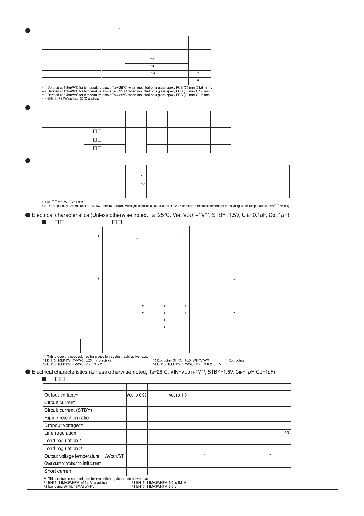
Absolute maximum ratings (Ta = 25 C)
Parameter Symbol Limits
Applied supply voltage
VMAX
-
0.3 ~
680 (HVSOF6)
Power dissipation
Pd
410 (HVSOF5)
540 (SSOP5)
-
Operating temperature range
Storage temperature range
Topr
Tstg
40
-
55
Recommended operating range
Parameter Min. Max. UnitTyp.Symbol
Power supply voltage
VIN
BH MA3W
Output current
BH FB1W
IOUT
BH LB1W
Recommended operating conditions
Parameter Min. Max. UnitTyp.Symbol
Input capacitor
Output capacitor
Noise decrease capacitor
CIN 0.1
Co
Cn
1.0
-
0.01 0.22
BHĄĄMA3WHFV series
Unit
+
6.5
+
~
85
+
~
125
2.5 5.5
-
--
--
--
-
-
-
-
V
mW
C
C
300
150 mA
150 mA
μF
μF
μF
Technical Note
V
mA
Conditions
Ceramic capacitor recommended
Ceramic capacitor recommended
Ceramic capacitor recommended
BH FB1WHFV/WG , BH LB1WHFV/WG
Parameter Symbol Min. Typ. Max. Unit Conditions
Output voltage
Circuit current
Circuit current(STBY)
Ripple rejection ratio
Load response 1
Load response 2
Dropout voltage
Line regulation
Load regulation
Load regulation
(1
(2
Over current protection
limit current
Short current
STBY pull-down resistor
STBY
control voltage
)
)
ON
OFF
1
VOU T
I GND
I STBY
LTV1
LTV2
3
VSAT
VDL1
VDL01
VDL02
ILMAX
I SHORT
RSTB
VSTBH
VSTBL
RR
V
OUT
150
150
550
-
-
-
-
-
-
-
-
-
-
-
-
1.5
0.3
0.99
I
OUT=1mA
VOUT
VOUT 1.01
40
70
50
50
250
2
10
15
3
250
5
300
50
40
1100
-
-
70
1.0
-
-
-
450
20
30
90
3
420
5
450
3
-
5
-
2200
Vcc
0.3
V
I
OUT=50mA
μA
STBY=0V
μA
VRR=-20dBv, fRR=1kHz, IOUT=10mA
dB
IOUT=1mA to 30mA
mV
I
OUT=30mA to 1mA
mV
V
mV
mV
mV
mA
3
mA
5
mA
IN=0.98 VOUT, IOUT=100mA
IN
=V
V
I
OUT=1mA to 100mA
I
OUT=1mA to 150mA
Vo=VOUT 0.98
V
o=0V
kΩ
V
V
BH MA3WHFV
Parameter Symbol Min. Typ. Max. Unit Conditions
V
OUT
I GND
I STBY
RR
VSAT1
VDL1
VDL01
VDL02
ILMAX
I SHORT
VOUT
-
-
-
-
-
-
-
-
-
-
65
60
60
18
±
100
600
100
95
-
1.0
-
90
2
6
20
30
90
ppm/
-
-
-
I
OUT=1mA
V
I
μA
OUT=1mA
μA
STBY=0V
dB
VRR=-20dBv, fRR=1kHz, IOUT=10mA
mV
VIN=0.98 X VOUT, IOUT=100mA
mV
VIN=VOUT+0.5V to 5.5V
mV
I
OUT=1mA to 100mA
mV
I
OUT=1mA to 300mA
C
IOUT=1mA, Ta=-40 to +85 C
mA
Vo=VOUT X 0.85
m
A
V
o=0V
+
0.5V to 5.5V
OUT
5
4
BH25,28,29,30,31,33WHFV/G
www.rohm.com
© 2010 ROHM Co., Ltd. All rights reserved.
2/8
2010.07 -
Rev. C
BH
□□
BH □□LB1WG series, BH□□LB1WHFV series,
FB1WG series, BH□□FB1WHFV series,
BH □□MA3WHFV
series
Technical Note
Typi cal charact eri st ic
s
• Output voltage-input volta ge
2
1.5
OUT[V]
1
Out put Voltage V
0.5
0
0 0.5 1 1.5 2 2.5 3 3.5 4 4.5 5 5.5
Input V oltage V
IN[V]
Fig.1
• GND c urrent
-
input volta ge
60
50
]
40
[DNGI tnerruC DNG μA
30
20
10
BH15 LB1WHFV
~ Co ndition ~
VIN=0 to 5.5V
Cin =0 .1μF
Co= 1.0 μF
ROUT=1 .5 kΩ
Ta= 2 5°C
BH15 LB1WHFV
~ Co ndition ~
VIN= 0
to
5.5V
Cin =0 .1μF
Co= 1.0 μF
ROUT=1 .5 k
Ta= 2 5°C
4
3
[V]
OUT
2
Out put Voltage V
1
0
0 0.5 1 1.5 2 2.5 3 3.5 4 4.5 5 5.5
Input V oltage V
Fig.2
60
50
]
Ω
40
[DNGI tnerruC DNG μA
30
20
10
IN[V]
BH28 FB1WHFV
~ Co ndition ~
VIN=0 to 5.5V
Cin =0 .1μF
Co= 1.0 μF
ROUT=2 .8 kΩ
Ta= 2 5°C
BH28 FB1WHFV
~ Condition ~
VIN= 0
to
5.5V
Cin =0 .1μF
Co= 1.0 μF
ROUT=2 .8 k
Ta= 2 5°C
4
3
2
Out put Voltage VOUT[V]
1
0
0 0.5 1 1.5 2 2.5 3 3.5 4 4.5 5 5.5
Input V oltage V
IN[V]
BH30MA3WH FV
~ Co ndition ~
VIN=0 to 5.5V
Cin =1 .0μF
Co= 1.0 μF
Cn= no ne
ROUT=3 .0 kΩ
Ta= 2 5°C
Fig.3
100
80
Ω
60
40
GN D Current IGND[μA]
20
BH30MA3WH FV
~ Co ndition ~
VIN= 0
to
5.5V
Cin =1 .0μF
Co= 1.0 μF
Cn= no ne
ROUT=3 .0 k
Ta= 2 5°C
Ω
0
0 0.5 1 1.5 2 2.5 3 3.5 4 4.5 5 5.5
• Output voltage
2
1.5
[V]
OUT
1
Out put Voltage V
0.5
0
0 100 200 300 400
• D ropout volta ge
500
400
]
300
200
Dropout Voltage VSAT[m V
100
Input V oltage VIN[V]
Fig.4
-
output curre nt
Output Curre nt IOUT[mA]
Fig.7
-
output curre nt
BH15 LB1WHFV
~ Co ndition ~
VIN=3.5V
VOUT=1.53V to 0V
Cin=0.1μF
Co=1.0μF
Ta= 25°C
BH28 FB1WHFV
~ Co ndition ~
VIN=2.74V
IOUT=0 to 150mA
Cin =0 .1μF
Co= 1.0 μF
Ta= 2 5°C
0
0 0.5 1 1.5 2 2.5 3 3.5 4 4.5 5 5.5
Input Voltage V
IN
[V]
Fig.5
3.5
3
2.5
[V]
OUT
2
1.5
Out put Voltage V
1
0.5
0
0 50 100 150 200 250 300
Output Curre nt I
OUT[mA]
Fig.8
300
250
200
150
100
Dropout Volt age VS A T [mV]
50
BH28 FB1WHFV
~ Co ndition ~
VIN=3.8V
VOUT=2.83V to 0V
Cin=0.1μF
Co=1.0μF
Ta= 25°C
BH30 MA3WHFV
~ Co ndition ~
VIN=2.940V
IOUT=0 to 300mA
Cin =1 .0μF
Co= 1.0 μF
Cn= no ne
Ta= 2 5°C
0
0 0.5 1 1.5 2 2.5 3 3.5 4 4.5 5 5.5
Input V oltage VIN[V]
Fig.6
3.5
3
2.5
2
1.5
Out put Voltage[V]
1
0.5
0
0 100 200 300 400 500 600 700
Output Curre nt IOUT[mA]
Fig.9
BH30MA3WH FV
~ Co ndition ~
VIN=4.0V
VOUT=3.03V to 0V
Cin=1.0μF
Co=1.0μF
Cn=none
Ta= 25°C
0
0 50 100 150
Output Curre nt I
OUT[mA]
Fig.10
www.rohm.com
© 2010 ROHM Co., Ltd. All rights reserved.
0
0 50 100 150 200 250 300
Output Curre nt I
OUT[mA]
Fig.11
3/8
2010.07 -
Rev. C

BH
□□
BH □□LB1WG series, BH□□LB1WHFV series,
FB1WG series, BH□□FB1WHFV series,
Typical Characteristics
-
• Output voltage
temperature
BH □□MA3WHFV
series
Technical Note
°
• Ripple reflection
-
frequency
Ω Ω Ω
°
°
Ω
°
°
°
Ω
°
°
Ω
°
• Load response characteristics (CO = 1.0 μF)
°
• Output voltage startup time
°
°
°
°
www.rohm.com
© 2010 ROHM Co., Ltd. All rights reserved.
4/8
2010.07 -
Rev. C

BH
□□
BH □□LB1WG series, BH□□LB1WHFV series,
FB1WG series, BH□□FB1WHFV series,
Block diagrams
BH □□MA3WHFV
series
Technical Note
Power supply input
Ground
Output voltage ON/OFF control
(High: ON, Low: OFF)
NO CONNECT
Voltage output
Output voltage ON/OFF control
(High: ON, Low: OFF)
Ground
Power supply input
Voltage output
NO CONNECT
Terminal No. Terminal Name
Function
Power supply input
Voltage output
Voltage output
Noise reducing capacitor
ground terminal
Ground
Output voltage ON/OFF control
(High: ON, Low: OFF)
Power dissipation Pd
1.
Power dissipation
Power dissipation calculation include estimates of power dissipation characteristics and internal IC power consumption
and should be treated as guidelines. In the event that the IC is used in an environment where this power dissipation is
exceeded, the attendant rise in the junction temperature will trigger the thermal shutdown circuit, reducing the current
capacity and otherwise degrading the IC's design performance. Allow for sufficient margins so that this power dissipation
is not exceeded during IC operation.
Calculating the maximum internal IC power consumption (P
MAX)
2. Power dissipation characteristics (Pd)
Board: 70 mm X 70 mm X 1.6 mm
Material: Glass epoxy PCB
Fig. 26: HVSOF6
Power Dissipation/
Power Dissipation Reduction (Example)
www.rohm.com
© 2010 ROHM Co., Ltd. All rights reserved.
Input voltage
Output voltage
Output current
Board: 70 mm
Material: Glass epoxy PCB
Fig. 27: HVSOF5
Power Dissipation/
Power Dissipation Reduction (Example)
X 70 mm X 1.6 mm
°°
5/8
Board: 70 mm X 70 mm X 1.6 mm
Material: Glass epoxy PCB
°
Fig. 28: SSOP5
Power Dissipation Reduction (Example)
Power Dissipation/
2010.07 -
Rev. C

BH
□□
BH □□LB1WG series, BH□□LB1WHFV series,
FB1WG series, BH□□FB1WHFV series,
BH □□MA3WHFV series
Technical Note
Input capacitor
It is recommended to insert bypass capacitors between input and GND pins, positioning them as close to the pins as
possible. These capacitors will be used when the power supply impedance increases or when long wiring routes are used, so
they should be checked once the IC has been mounted.
Ceramic capacitors generally have temperature and DC bias characteristics. When selecting ceramic capacitors, use X5R or
X7R or better models that offer good temperature and DC bias characteristics and high torelant voltages.
Examples of ceramic capacitor characteristics
120
100
80
60
10V torelance
40
50V torelance
16V torelance
100
50V torelance
95
90
16V torelance
85
10V torelance
80
120
100
80
60
40
Y5V
X7R
X5R
20
0
Rate of change in electrostatic capacitance (%)
Fig. 29: Capacitance-bias
1234
0
DC bias Vdc (V)
characteristics (Y5V) Fig. 30: Capacitance-bias
75
70
Rate of change in electrostatic capacitance (%)
1234
0
DC bias Vdc (V)
characteristics (X5R, X7R) Fig. 31: Capacitance–temperature characteristics
20
0
Rate of change in electrostatic capacitance (%)
-
0 255075
25
Temperature (°C)
(X5R, X7R, Y5V)
Output capacitor
To prevent oscillation at the output, it is recommended that the IC be operated at the stable region show in below Fig. It
operates at the capacitance of more than 1.0μF. As capacitance is larger, stability becomes more stable and characteristic of
output load fluctuation is also improved.
BHŜŜLB1WHFV/WG
Cout=1.0μF
100
10
1
ESR(Ω)
0.1
0.01
0 50 100 150
Fig. 32 BHŜŜLB1WHFV/WG
Stable operating region characteristics (Example)
Ta=+25°C
Stable region Stable region
Output current IOUT(mA)
BHŜŜFB1WHFV/WG
Cout=2.2μF
100
10
1
ESR(Ω)
0.1
0.01
0 50 100 150
Fig. 33 BHŜŜFB1WHFV/WG
Stable operating region characteristics (Example)
Ta=+25°C
Output current IOUT(mA)
BHŜŜMA3WHFV
Cout=1.0μF Cin=1.0μF
100
10
1
ESR(Ω)
0.1
0.01
0 100 200 300
Fig. 34 BHŜŜMA3WHFV
Stable operating region characteristics (Example)
Stable region
Output current IOUT(mA)
Ta=+25°C
Other precautions
• Over current protection circuit
The IC incorporates a built-in over current protection circuit that operates according to the output current capacity. This circuit
serves to protect the IC from damage when the load is shorted. The protection circuits use fold-back type current limiting and
are designed to limit current flow by not latching up in the event of a large and instantaneous current flow originating from a
large capacitor or other component. These protection circuits are effective in preventing damage due to sudden and
unexpected accidents. Howeve r, the IC should not be used in applications characterized by the continuous operation or
transitioning of the protection circuits.
• Thermal shutdown circuit
This system has a built-in thermal shutdown circuit for the purpose of protecting the IC from thermal damage. As shown
above, this must be used within the range of power dissipation, but if the power dissipation happens to be continuously
exceeded, the chip temperature increases, causing the thermal shutdown circuit to operate. When the thermal shutdown
circuit operates, the operation of the circuit is suspended. The circuit resumes operation immediately after the chip
temperature decreases, so the output repeats the ON and OFF states. There are cases in which the IC is destroyed due to
thermal runaway when it is left in the overloaded state. Be sure to avoid leaving the IC in the overloaded state.
• Actions in strong magnetic fields
Use caution when using the IC in the presence of a strong magnetic field as such environments may occasionally cause the chip
to malfunction.
• Back current
In applications where the IC may be exposed to back current flow, it is recommended to create a route t dissipate this current
by inserting a bypass diode between the V
IN and VOUT pins.
• GND potential
Ensure a minimum GND pin potential in all operating conditions.
In addition, ensure that no pins other than the GND pin carry a voltage less than or equal to the GND pin, including during
actual transient phenomena.
www.rohm.com
© 2010 ROHM Co., Ltd. All rights reserved.
6/8
2010.07 -
Rev. C

BH
□□
BH □□LB1WG series, BH□□LB1WHFV series,
FB1WG series, BH□□FB1WHFV series,
BH □□MA3WHFV series
Technical Note
Noise terminal (BHŜŜMA3WHFV)
The terminal is directly connected to inward normal voltage source. Because this has low current ability, load exceeding
100nA will cause some instability at the output. For such reasons, we urge you to use ceramic capacitors which have less
leak current. When choosing noise the current reduction capacitor, there is a trade-off between boot-up time and stability. A
bigger capacitor value will result in lesser oscillation but longer boot-up time for VOUT.
100
10
1
0.1
VOUT startup time t (msec)
0.01
100P 1000P 0.01μ 0.1μ
noise-filtering capacitor capacitance Cn (F)
Fig. 35: VOUT startup time vs. noise-filtering capacitor capacitance characteristics (Example)
BH30MA3WHFV
~ Condition ~
VIN=4.0V
Cin=1.0μF
Co=1.0μF
ROUT=3.0kΩ
Ta=25°C
Regarding input pin of the IC
This monolithic IC contains P
+ isolation and P substrate layers between adjacent
elements in order to keep them isolated. P/N junctions are formed at the intersection of
these P layers with the N layers of other elements to create a variety of parasitic elements.
For example , when a resistor and transistor are connected to pins as sho wn in Fig.37
The P/N junction functions as a parasitic diode when GND > (Pin A) for the resistor or
GND > (Pin B) for the transistor (NPN).
Similarly, when GND > (Pin B) for the transistor (NPN), the parasitic diode described
above combines with the N lay er of other adjacent elements to oper ate as a par asitic
NPN transistor.
The formation of parasitic elements as a result of the relationships of the potentials of
different pins is an inevitable result of the IC's architecture. The operation of parasitic
elements can cause interference with circuit operation as well as IC malfunction and
damage. For these reasons, it is necessary to use caution so that the IC is not used in a
way that will trigger the operation of parasitic elements, such as by the application of
voltage lower than the GND (P substrate) voltage to input pins.
back current
VCC
CTL
OUT
GND
Fig. 36: Example of bypass
diode connection
(Terminal A)
+
P
N
P
Resistor
N
P-board
Part number selection
BH 3 FB1 W HFV0
ROHM
part number
Output
voltage
P
Parasitic element
GND
+
P
N
Current capacity
MA3 : 300mA
FB1 : 150mA
LB1 : 150m
(Terminal B)
P
Parasitic elements
A
B
O
+
E
N
N
Fig.37
Shutdown
switch
W : With switch
Transistor (NPN)
P
P
GND
GND
+
P
NN
Package
HFV : HVSOF6
HVSOF5
SSOP5
G :
(Terminal B)
B
Other adjacent elements
(Terminal A)
GND
-T
R
Package specification
TR : Embossed taping
C
E
GND
Parasitic elements
Parasitic element
www.rohm.com
© 2010 ROHM Co., Ltd. All rights reserved.
7/8
2010.07 -
Rev. C

BH
□□
BH □□LB1WG series, BH□□LB1WHFV series,
FB1WG series, BH□□FB1WHFV series,
(Unit:mm) (Unit:mm) (Unit:mm)
+6°
4°
-
4°
4
0.42
0.2Min.
+0.05
0.13
-0.03
+0.05
-0.04
0.1
3
1.0±
2.8±0.2
1.25Max.
1.1±0.05
2.9±0.2
5
-0.1
+0.2
1.6
12
0.95
0.05±0.05
BH □□MA3WHFV series
1.6±0.05
0.8
0.3
(0.05)
0.05
±0.05
1.6
5
123
±0.05
1.2
(1.28MAX.)
0.6Max.
0.5
4
0.22±0.05
(0.91)
4
321
(0.41)
0.2Max.
5
0.13±0.05
0.1
±
3.0
0.1
±
2.6
HVSOF5SSOP5 HVSOF6
(1.8MAX.)
1.6±0.1
0.75Max.
(2.8MAX.)
0.5
Technical Note
(1.5)
456
321
S
0.22±0.05
(1.2)
(1.4)
(0.45)
(0.15)
0.1 S
0.145±0.05
(Package Specification) SSOP5, HVSOF5
Package Form
Package Quantity
Package
Orientation
Embossed taping
3000pcs
TR
(When the reel is held with the left hand and the tape is drawn out with the right hand,
the No. 1 pin of the product faces the upper right direction.)
Reel
No. 1 pin
* Please make orders in multiples of the package quantity.
Pulling side
(Package Specification) HVSOF6
Package Form
Package Quantity
Package
Orientation
Embossed taping
3000pcs
TR
(When the reel is held with the left hand and the tape is drawn out with the right hand,
the No. 1 pin of the product faces the upper right direction.)
* Please make orders in multiples of the package quantity.
www.rohm.com
© 2010 ROHM Co., Ltd. All rights reserved.
8/8
2010.07 -
Rev. C

Notes
No copying or reproduction of this document, in part or in whole, is permitted without the
consent of ROHM Co.,Ltd.
The content specied herein is subject to change for improvement without notice.
The content specied herein is for the purpose of introducing ROHM's products (hereinafter
"Products"). If you wish to use any such Product, please be sure to refer to the specications,
which can be obtained from ROHM upon request.
Examples of application circuits, circuit constants and any other information contained herein
illustrate the standard usage and operations of the Products. The peripheral conditions must
be taken into account when designing circuits for mass production.
Great care was taken in ensuring the accuracy of the information specied in this document.
However, should you incur any damage arising from any inaccuracy or misprint of such
information, ROHM shall bear no responsibility for such damage.
The technical information specied herein is intended only to show the typical functions of and
examples of application circuits for the Products. ROHM does not grant you, explicitly or
implicitly, any license to use or exercise intellectual property or other rights held by ROHM and
other parties. ROHM shall bear no responsibility whatsoever for any dispute arising from the
use of such technical information.
Notice
The Products specied in this document are intended to be used with general-use electronic
equipment or devices (such as audio visual equipment, ofce-automation equipment, communication devices, electronic appliances and amusement devices).
The Products specied in this document are not designed to be radiation tolerant.
While ROHM always makes efforts to enhance the quality and reliability of its Products, a
Product may fail or malfunction for a variety of reasons.
Please be sure to implement in your equipment using the Products safety measures to guard
against the possibility of physical injury, re or any other damage caused in the event of the
failure of any Product, such as derating, redundancy, re control and fail-safe designs. ROHM
shall bear no responsibility whatsoever for your use of any Product outside of the prescribed
scope or not in accordance with the instruction manual.
The Products are not designed or manufactured to be used with any equipment, device or
system which requires an extremely high level of reliability the failure or malfunction of which
may result in a direct threat to human life or create a risk of human injury (such as a medical
instrument, transportation equipment, aerospace machinery, nuclear-reactor controller, fuelcontroller or other safety device). ROHM shall bear no responsibility in any way for use of any
of the Products for the above special purposes. If a Product is intended to be used for any
such special purpose, please contact a ROHM sales representative before purchasing.
If you intend to export or ship overseas any Product or technology specied herein that may
be controlled under the Foreign Exchange and the Foreign Trade Law, you will be required to
obtain a license or permit under the Law.
www.rohm.com
© 2010 ROHM Co., Ltd. All rights reserved.
Thank you for your accessing to ROHM product informations.
More detail product informations and catalogs are available, please contact us.
ROHM Customer Support System
http://www.rohm.com/contact/
R1010
A
 Loading...