

Page 1
Ambient Light Sensor ICs
Digital 16bit Serial Output Type
Ambient Light Sensor IC
BH1730FVC
●Descriptions
BH1730FVC is a digital Ambient Light Sensor IC for I
data for adjusting LCD backlight power of TV, mobile phone. It is possible to detect very wide range light intensity. (0.008 65535 lx ).
●Features
●Applications
●Absolute Maximum Ratings
●Operating Conditions
2
1) I
2) There are two outputs that peaks of a spectrum response are in visible light (Type0) and in infrared light (Type1).
3) Illuminance to Digital Converter
4) Very wide range and High resolution. ( 0.008 - 65535 lx )
5) Low Current by power down function
6) 50Hz / 60Hz light noise reject-function
7) Correspond to 1.8V logic input interface
8) Light source dependency is little by calculating with Type0 and Type1.
( ex. Incandescent Lamp. Fluorescent Lamp. Halogen Lamp. White LED. Sun Light )
9) Interrupt function is available.
10) Adjustable measurement result for influence of optical window
( It is possible to detect min. 0.001 lx, max. 100000 lx by using this function. )
11) Small measurement variation (+/- 15%)
12) Built in power on reset circuit.
LCD TV, Mobile phone, NOTE PC, Portable game machine, Digital camera, Digital video camera, PDA, LCD display
C bus Interface ( f / s Mode Support, Slave address "0101001". )
Parameter Symbol Limits Units
Supply Voltage VCCmax
INT , SDA, DVI, SCL, Terminal Voltage V
Operating Temperature Topr -40~70 ℃
Storage Temperature Tstg -40~100 ℃
SDA, INT Sink Current Imax 7 mA
Power Dissipation Pd 260※ mW
※ 70mm × 70mm × 1.6mm glass epoxy board. Derating in done at 3.47mW/℃ for operating above Ta=25℃.
Parameter Symbol Min. Typ. Max. Units
VCC Voltage Vcc 2.4 3.0 3.6 V
I2C Reference Voltage VDVI 1.65 - VCC V
2
C bus interface. This IC is the most suitable to obtain the ambient light
4.5 V
7 V
max, V
INT
SDA
max, V
max, V
DVI
SCL
max
No.11046EAT13
www.rohm.com
© 2012 ROHM Co., Ltd. All rights reserved.
1/20
2012.02 - Rev.A
Page 2

BH1730FVC
1
1
1
●Electrical Characteristics ( VCC = 3.0V, VDVI = 3.0V, Ta = 25℃, unless otherwise noted )
Parameter Symbol
Min. Typ. Max.
Limits
Units Conditions
Ev = 100 lx
Supply Current Icc1 - 150 200 uA
CONTROL register(00h) = ”03h”
and the other registers are default.
Powerdown Current Icc2 - 0.85 1.5 uA
No input Light
All registers are default.
Peak Wave Length in Type0 λp0 - 600 - nm Visible light response
Technical Note
※
Peak Wave Length in Type1 λp1 - 840 - nm Infrared light response
※
※
ADC count value in Type0 D1k_0 1020 1200 1380 count
ADC count value in Type1 D1k_1 153 180 207 count
EV = 1000 lx
TIMING register(01h) = “DAh”
GAIN register(07h) = “00h”
EV = 1000 lx
TIMING register(01h) = “DAh”
GAIN register(07h) = “00h”
No input Light
Dark ( 0 lx ) Sensor out in Type0 S0_0 0 0 2 count
TIMING register(01h) = “DAh”
GAIN register(07h) = “00h”
No input Light
Dark ( 0 lx ) Sensor out in Type1 S0_1 0 0 2 count
TIMING register(01h) = “DAh”
GAIN register(07h) = “00h”
Gain X1 resolution in Type0 rG1 - 0.83 - lx/count TIMING register(01h) = “DAh”
Gain X2 resolution in Type0 rG2 - 0.42 - lx/count TIMING register(01h) = “DAh”
Gain X64 resolution in Type0 rG64 - 0.014 - lx/count TIMING register(01h) = “DAh”
Gain X128 resolution in Type0 rG128 - 0.007 - lx/count TIMING register(01h) = “DAh”
Measurement Time tmt1 - 100 150 ms TIMING register(01h) = “DAh”
Incandescent / Fluorescent ratio
by calculating with Type0 and
rIF - 1 - times EV = 1000 lx
Type1
INT Output ‘L’ Voltage VINT 0 - 0.4 V IINT = 3 mA
DVI Input ‘L’ Voltage VDVL - - 0.4 V
SCL, SDA Input ‘H’ Voltage 1 VIH1 0.7*DVI - - V DVI ≧ 1.8V
1
※
1
※
1
※
1
※
SCL, SDA Input ‘H’ Voltage 2 VIH2 1.26 - - V 1.65V ≦ DVI <1.8V
SCL, SDA Input ‘L’ Voltage 1 VIL1 - - 0.3*DVI V DVI ≧ 1.8V
SCL, SDA Input ‘L’ Voltage 2 VIL2 - - DVI–1.26 V 1.65V ≦ DVI < 1.8V
SCL, SDA, INT Input ‘H’ Current IIH - - 10 µA
SCL, SDA, INT Input ‘L’ Current IIL - - 10 µA
I2C SCL Clock Frequency fSCL - - 400 kHz
I2C Bus Free Time tBUF 1.3 - - µs
I2C Hold Time ( repeated ) START
Condition
I2C Set up time for a Repeated
START Condition
I2C Set up time for STOP
Condition
tHDSTA 0.6 - - µs
tSUSTA 0.6 - - µs
tSUSTO 0.6 - - µs
I2C Data Hold Time tHDDAT 0 - 0.9 µs
I2C Data Setup Time tSUDAT 100 - - ns
I2C ‘L’ Period of the SCL Clock tLOW 1.3 - - µs
I2C ‘H’ Period of the SCL Clock tHIGH 0.6 - - µs
I2C SDA Output ‘L’ Voltage VOL 0 - 0.4 V IOL = 3 mA
※1 White LED is used as optical source.
www.rohm.com
© 2012 ROHM Co., Ltd. All rights reserved.
2/20
2012.02 - Rev.A
Page 3
BH1730FVC
l
Technical Note
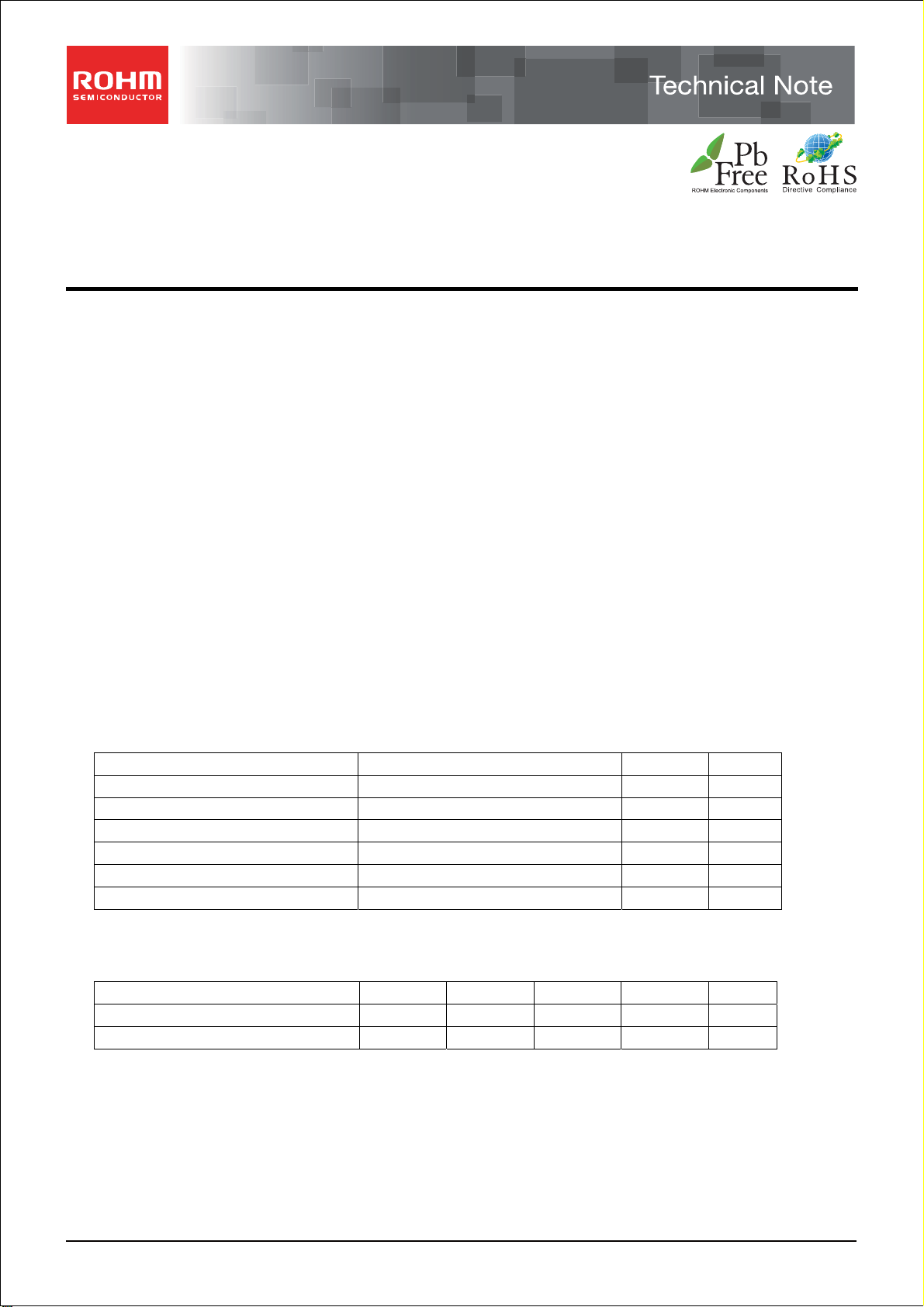
●Reference Data
1.2
1
0.8
0.6
Ratio
0.4
0.2
0
400 500 600 700 800 900 1000 1100
Wavelength [ nm ]
Fig.1 Spectral Response of Type0
(visible light peak)
10
8
6
4
Measurement Result
2
0
-40-20 0 20406080
Fig.4 Dark Response of Type0
Ta [ ℃ ]
1.2
1
0.8
0.6
Ratio
0.4
0.2
0
-40-20020406080
Fig.7 ADC count value in Type0
Temperature Dependency
Ta [ ℃ ]
10
1
ICC @ POWER DOWN [ uA
0.1
-40-200 20406080
Ta [ ℃ ]
Fig.10 Power down ICC@0Lx
Temperature Dependency
1.2
1
0.8
0.6
Ratio
0.4
0.2
0
400 500 600 700 800 900 1000 1100
Wavelength [ nm ]
Fig.2 Spectral Response of Type1
(infrared light peak)
1.2
1
0.8
0.6
Ratio
0.4
0.2
0
-90 -60 -30 0 30 60 90
1pin
-
-
Ang le [ deg ]
+
+
Fig.5 Directional Characteristics 1
Fl uoresc ent
Lig ht
Incandes cent
Lig ht
Halogen
Lig ht
Kripton Li ght
White LED
00.511.52
Ratio
Fig.8 Light Source Dependency in
calculation from Type0 and Type1.
( Fluorescent Light is set to '1' )
1.2
1
0.8
0.6
Ratio
0.4
0.2
0
2 2.5 3 3.5 4
DVI=1.8V
VCC [ V ]
Fig.11 Measurement Result
VCC Dependency
100000
10000
1000
100
Measurement Resu
10
1
1 10 100 1000 10000 100000
Illumi nance [ l x ]
Fig.3 Illuminance -Measurement
Result of Type0, Gain 1X, ITIME=DAh
1.2
1
0.8
0.6
Ratio
0.4
0.2
0
-90 -60 -30 0 30 60 90
Ang le [ deg ]
-
1pin
-
+
+
Fig.6 Directional Characteristics 2
300
250
200
150
100
ICC @ Measuremen
50
0
2 2.5 3 3.5 4
VCC [ V ]
Fig.9 VCC - ICC
( During measurement )
1.2
1
0.8
0.6
Ratio
0.4
0.2
0
1.5 2 2.5 3 3.5
VCC=3V
DVI [ V ]
Fig.12 Measurement Result
DVI Dependency
www.rohm.com
© 2012 ROHM Co., Ltd. All rights reserved.
3/20
2012.02 - Rev.A
Page 4
BH1730FVC
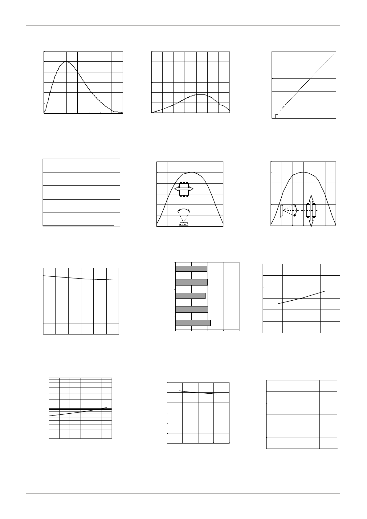
●Block Diagram
●Block Diagram Descriptions
・PD
Photo diodes (PD) with peaks in visible light and in infrared light.
・AMP
Integration OPAMP for converting from PD current to voltage.
・ADC
AD converter for obtainment digital 16bit data.
・ADC Logic + I
2
C Interface + INT Interface
Ambient light calculation logic and I
・OSC
Internal oscillator ( typ. 360kHz ). It is clock for internal logic.
・POR
Power on reset. All register is reset after VCC is supplied. Please refer P14 (Caution of power on reset function).
AMP
PD for visible light
AMP
PD for infrared light
2
C Bus Interface and Interrupt function Interface.
VCC
ADC
ADC
OSC
GND
DVI
ADC Logic
+
2
I
C Interface
+
INT Interface
INT
Technical Note
SCL
SDA
POR
www.rohm.com
© 2012 ROHM Co., Ltd. All rights reserved.
4/20
2012.02 - Rev.A
Page 5
BH1730FVC
Technical Note
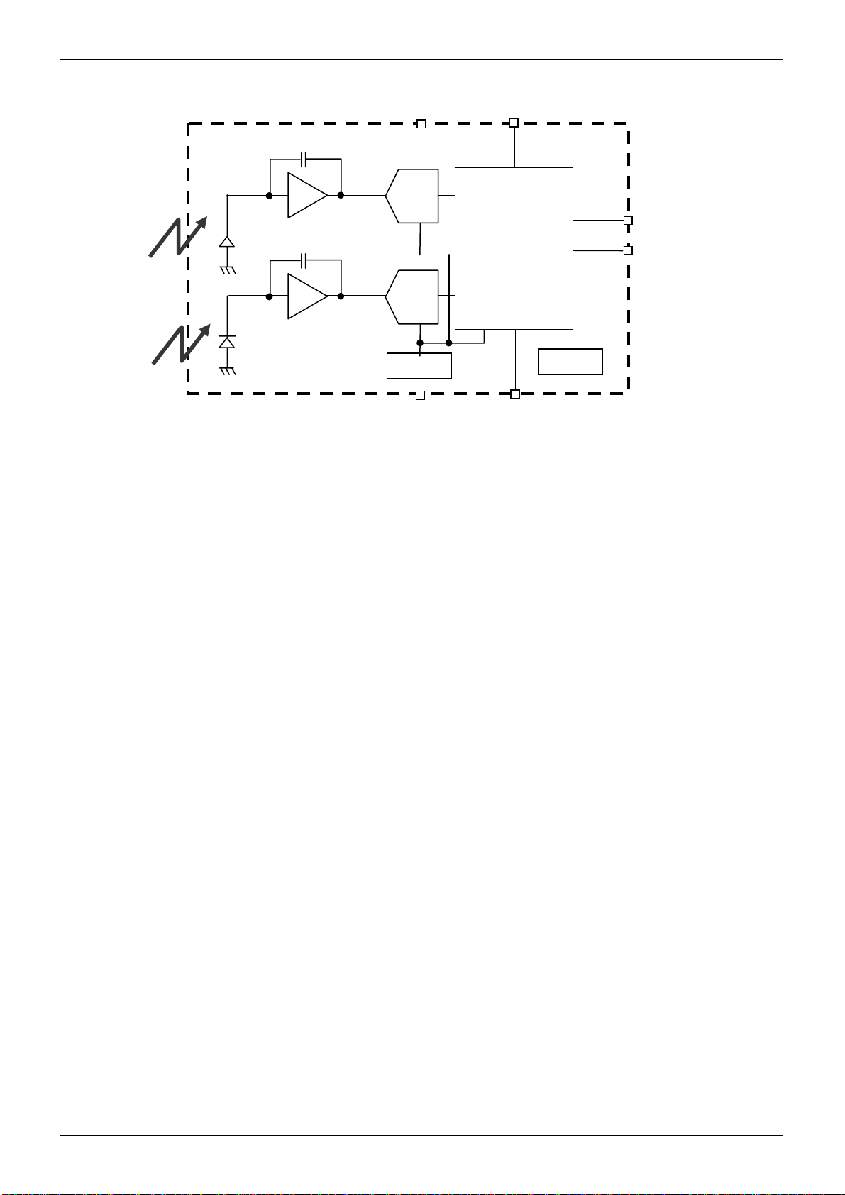
●I2C Bus Access and Write / Read format
2
C Bus interface timing chart
1 ) I
Write measurement command and Read measurement result are done by I
specification of I
2
C Bus interface, and follow the formally timing chart.
2
C Bus interface. Please refer the formally
SDA
tf
t
LOW
t
tr
SU ; DAT
t
f
t
HD ; STA
SCL
S
t
HD ; STA
t
HD ; DAT
t
HIGH
t
SU ; STA
Sr
t
SU;STO
2) Main write Format
1. Case of “Write to Command Register”
ST
Slave Address
0101001
W
0
ACK
Data to Command Register
1XXXXXXX
2. Case of “Write to Data Register”
ST
Slave Address
0101001
W
0
ACK
Data specified at register address field
0XXXXXXX
Data specified at register address
field +1
ACK
・・・ ACK
Data specified at register address
field +N
※ The register address that set in Command register is used.
3. Case of "write to data register after write to Command Register"
ST
Slave Address
0101001
W
0
ACK
Data to Command Register
1XXXXXXX
Data specified at register address
field
ACK
・・・ ACK
Data specified at register address
field +N
3) Main read Format
ST
Slave Address
0101001
R
ACK Data specified at register address field
1
Data specified at register
address field +1
ACK ・・・ ACK
Data specified at register
address field +N
※ The register address that set in Command register is used.
from master to slave
from slave to master
BH1730FVC operates as I2C bus slave device.
※
Please refer formality I2C bus specification of NXP semiconductor
※
BH1730FVC continues to write or read data with address increments until master issues stop condition.
Read cycle is 00h - 01h - 02h - 03h - 04h - 05h - 06h – 07h – 12h – 14h – 15h – 16h – 17h - 00h ………
tr
t
BUF
P
ACK
SP
ACK
ACK
SP
ACK
ACK
SP
ACK
NACK SP
S
www.rohm.com
© 2012 ROHM Co., Ltd. All rights reserved.
5/20
2012.02 - Rev.A
Page 6
BH1730FVC
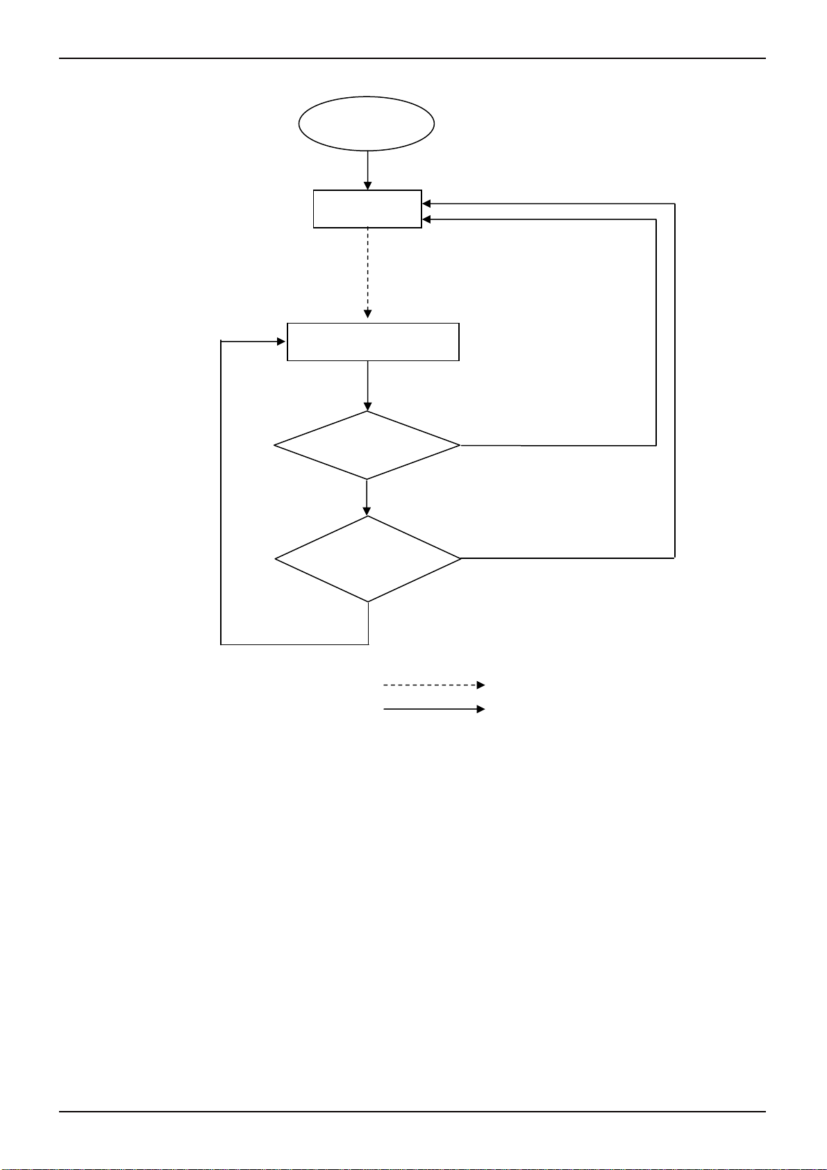
●Measurement Procedure
●Explanation of Asynchronous reset and Software reset command.
1) Asynchronous reset
All registers are reset and BH1730FVC becomes power down during DVI = 'L'. Initial reset is not necessary, because
power on reset function is included in this product.
2) Software reset command
All registers are reset and BH1730FVC becomes power down by Software reset command.
Power supply
Power Down
POWER bit = H and
ADC_EN bit =H
Measurement
ONE_TIME bit = H?
No
INT_STOP bit = H and
INT is active?
No
Initial state is Power Down mode after
VCC and DVI supply.
Yes
Yes
State Transition by I2C write-command.
Automatically State Transition
Technical Note
www.rohm.com
© 2012 ROHM Co., Ltd. All rights reserved.
6/20
2012.02 - Rev.A
Page 7
BH1730FVC
●Command set
Address Type Register name Register function
-- W COMMAND Specifies register address or set special command
00h RW CONTROL Operation mode control
01h RW TIMING Light integration time control
02h RW INTERRUPT Interrupt function control
03h RW THLLOW Low byte of low interrupt threshold setting
04h RW THLHIGH High byte of low interrupt threshold setting
05h RW THHLOW Low byte of high interrupt threshold setting
06h RW THHHIGH High byte of high interrupt threshold setting
07h RW GAIN Gain control
12h R ID Part number and Revision ID
14h R DATA0LOW ADC Type0 low byte data register
15h R DATA0HIGH ADC Type0 high byte data register
16h R DATA1LOW ADC Type1 low byte data register
17h R DATA1HIGH ADC Type1 high byte data register
○COMMAND
7 6 5 4 3 2 1 0
CMD TRANSACTION ADDRESS / Special command
Field
CMD 7
TRANSACTION 6 : 5 W
ADDRESS
Special command
Bit
Type Description
W
4 : 0 W
Write 1
00 : COMMAND<4:0> is ADDRESS field.
01 : Reserved.
10 : Reserved.
11 : COMMAND<4:0> is Special command field.
Specify register address.
Don’t specify invalid register address.
00001 : Interrupt output reset.
00010 : Stop manual integration mode.
00011 : Start manual integration mode.
00100 : Software reset
Don’t input other commands.
Technical Note
default value 00h
www.rohm.com
© 2012 ROHM Co., Ltd. All rights reserved.
7/20
2012.02 - Rev.A
Page 8

BH1730FVC
○CONTROL (00h)
7 6 5 4 3 2 1 0
Field
RES 7: 6
ADC_INTR 5 R
ADC_VALID 4 R
ONE_TIME 3 RW
DATA_SEL 2 RW
ADC_EN 1 RW
POWER 0 RW
○TIMING (01h)
7 6 5 4 3 2 1 0
Field
ITIME 7 : 0
RES
ADC_
INTR
Bit
Type Description
RW
Bit
Type Description
RW
ADC_
VAL ID
Write 00
0 : Interrupt is inactive.
1 : Interrupt is active.
0 : ADC data is not updated after last reading.
1 : ADC data is updated after last reading.
0 : ADC measurement is continuous.
1 : ADC measurement is one time.
ADC changes to power down automatically.
0 : ADC measurement Type0 and Type1.
1 : ADC measurement Type0 only.
0 : ADC measurement is not started.
1 : ADC measurement is started.
0 : ADC power down.
1 : ADC power on.
ADC Light Integration time control.
00000000 : Use manual integration mode.
11111111 : 1 c y c l e. 2.7ms.
11111110 : 2 c y c le. 5.4m s .
11101101 : 19 cycle. 51.3ms.
11011010 : 38 cycle. 102.6ms.
10110110 : 74 cycle. 199.8ms.
01101100 : 148 cycle. 399.6ms.
00000001 : 255 cycle. 688.5ms.
Cycle is defined 256-ITIME<7:0>.
Integration time is typically cycle*2.7ms.
ADC needs additional 2ms for internal calculation.
ITIME
ONE_
TIME
DATA_
SEL
ADC_
EN
Technical Note
POWER
default value 00h
default value DAh
www.rohm.com
© 2012 ROHM Co., Ltd. All rights reserved.
8/20
2012.02 - Rev.A
Page 9

BH1730FVC
○INTERRUPT (02h)
7 6 5 4 3 2 1 0
RES
Field
RES
INT_STOP
RES
INT_EN
PERSIST
○TH_LOW (03h,04h)
7 6 5 4 3 2 1 0
Register Address Bit
TH lower LSBs 03h 7 : 0 RW Lower byte
TH lower MSBs 04h 7 : 0 RW Upper byte
○TH_UP (05h,06h)
7 6 5 4 3 2 1 0
Register Address Bit
TH upper LSBs 05h 7 : 0 RW Lower byte
TH upper MSBs 06h 7 : 0 RW Upper byte
○GAIN (07h)
7 6 5 4 3 2 1 0
Field
RES 7 : 3
GAIN 2 : 0 RW
INT_
STOP
Technical Note
RES
Bit
Type Description
7
RW Write 0.
6
RW
5
RW Write 0.
4
RW
3 : 0
RW
RES GAIN
Bit
Type Description
RW
INT_
EN
0 : ADC measurement is continuous.
1 : ADC measurement is stopped and ADC becomes
power down state when interrupt becomes active.
0 : Interrupt function is invalid.
1 : Interrupt function is valid.
Interrupt persistence function.
0000 : Interrupt becomes active at each measurement end.
0001 : Interrupt status is updated at each measurement end.
0010 : Interrupt status is updated if two consecutive threshold
judgments are the same.
When set 0011 or more, interrupt status is updated if threshold
judgments are the same over consecutive set times.
Lower threshold data
PERSIST
default value 00h
default value 00h
Type Description
Upper threshold data
default value FFh
Type Description
default value 00h
Write 00000.
Change ADC resolution.
X00 : X1 gain mode
X01 : X2 gain mode
X10 : X64 gain mode
X11 : X128 gain mode
www.rohm.com
© 2012 ROHM Co., Ltd. All rights reserved.
9/20
2012.02 - Rev.A
Page 10

BH1730FVC
○PART_ID ( 12h )
7 6 5 4 3 2 1 0
Field Bit Type Description
Part number 7 : 4
Revision ID 3 : 0 R XXXX
○DATA0 (14h,15h)
7 6 5 4 3 2 1 0
Register Address Bit
DATA0 LSBs 14h 7 : 0 R Lower byte
DATA0 MSBs 15h 7 : 0 R Upper byte
○DATA1 (16h,17h)
7 6 5 4 3 2 1 0
Register Address Bit
DATA1 LSBs 16h 7 : 0 R Lower byte
DATA1 MSBs 17h 7 : 0 R Upper byte
Part Number Revision ID
R
0111
ADC Type0 data
Type Description
ADC Type1 data
Type Description
Technical Note
default value 7Xh
default value 00h
default value 00h
www.rohm.com
© 2012 ROHM Co., Ltd. All rights reserved.
10/20
2012.02 - Rev.A
Page 11

BH1730FVC
Technical Note
●Measurement sequence example from "Write to start measurement" to "Read measurement result"
from Master to Slave
from Slave to Master
① Send "Continuous measurement mode" instruction
ST
Slave Address
0101001
W
0
ACK
Write Command Register
1000_0000
Write CONTROL register
0000_0011
② Wait to complete 1st measurement. TIMING=DAh (typ. 100ms, max.150ms) and GAIN=00h (X1 Gain) at default.
③ Read measurement result.
ST
Slave Address
0101001
W
0
ACK
Write Command Register
1001_0100
ST
Slave Address
0101001
R
ACK Read DATA0 LSBs register
1
ACK
ACK
ACK
ACK
SP
SP
Read DATA0 MSBs register
●Application circuit example
If you don't use INT Pin, please connect to GND or open.
INT pin pull up resister
0.1µF
100kohm
BH1730FVC
VCC
INT
GND
Micro
Controller
SCL
DVI
SDA
ACK Read DATA1 LSBs register ACK
Read DATA1 MSBs register
NACK
I2C bus pull up resister
2.2kΩ
2.2kΩ
I2C bus voltage source
0.1µF
SP
www.rohm.com
© 2012 ROHM Co., Ltd. All rights reserved.
11/2 0
2012.02 - Rev.A
Page 12

BH1730FVC
●Lux calculation from DATA0 and DATA1
BH1730FVC has two outputs, DATA0 (14h, 15h) for detecting visible light and infrared light, and DATA1 (16h, 17h) for
detecting infrared light. Lux value can be calculated by using these two outputs. The calculation formula depends on the
characteristic of optical window. The example of the calculation is shown as follows.
Ex) No optical window or optical window that has flat transmittance from visible light to infrared light.
if (DATA1/DATA0<0.26) Lx = ( 1.290*DATA0 - 2.733*DATA1 ) / Gain * 100ms / ITIME
else if (DATA1/DATA0<0.55) Lx = ( 0.795*DATA0 - 0.859*DATA1 ) / Gain * 100ms / ITIME
else if (DATA1/DATA0<1.09) Lx = ( 0.510*DATA0 - 0.345*DATA1 ) / Gain * 100ms / ITIME
else if (DATA1/DATA0<2.13) Lx = ( 0.276*DATA0 - 0.130*DATA1 ) / Gain * 100ms / ITIME
else Lx=0
Technical Note
www.rohm.com
© 2012 ROHM Co., Ltd. All rights reserved.
12/20
2012.02 - Rev.A
Page 13

BH1730FVC
● Interrupt function
Interrupt function compares measurement result to preset interrupt threshold level. BH1730FVC uses two threshold level
(upper and lower ). If measurement result is outside of two threshold, INT pin outputs ’L’. Interrupt threshold is defined at
Interrupt threshold registers ( 03h - 06h ).
Interrupt function is able to control by Interrupt opecode. Interrupt persistence is defined at Interrupt opecode lower 4 bits.
INT pin is Nch open drain terminal so this terminal should be pull-up to some kind of voltage source by an external resister.
Maximum sink current rating of this terminal is 7mA.
INT terminal is high impedance when VCC is supplied.
INT terminal becomes inactive by setting “Interrupt output reset” special command. VCC current (approximately 30uA at
VCC=3.0V ) is consumed during INT terminal is ‘L’. So it is recommended to reset INT terminal at once when interrupt is
detected.
Master writes “Interrupt output reset” command.
Technical Note
INT Terminal
persistence = 1
persistence = 2
DATA0
Interrupt threshold H level
H
L
H
L
Interrupt threshold L level
www.rohm.com
© 2012 ROHM Co., Ltd. All rights reserved.
sequential measurement results
13/20
time
2012.02 - Rev.A
Page 14

BH1730FVC
●Caution of power on reset function
BH1730FVC has power on reset ( POR ) function. POR is to reset all register and flip flop when VCC Power supplies.
There is some cautions about power on and down sequence seeing in below.
① Power on time : t1
More than 2ms is need to active BH1730FVC after VCC supplies more than 2.0V from VCC is less than 0.4V.
② Power off time : t2
More than 1ms (VCC < 0.4V) is need to active BH1730FVC.
VCC
BH1730FVC
*”active state” is that BH1730FVC works and accept I2C bus access correctly.
2.0V
0.4V
Don’t care
t1
active
t2
Don’t care
t1
Technical Note
active
www.rohm.com
© 2012 ROHM Co., Ltd. All rights reserved.
14/20
2012.02 - Rev.A
Page 15

BH1730FVC
●ALS sensitivity adjustment function
BH1730FVC is possible to change ALS sensitivity. And it is possible to cancel the optical window influence (difference with /
without optical window ) by using this function. Adjustment is done by changing measurement time. For example, when
transmission rate of optical window is 50% (measurement result becomes 0.5 times if optical window is set), influence of
optical window is ignored by changing sensor sensitivity from default to 2 times.
Sensitivity can be adjusted by ITIME (01h<7:0>). The measurement time is proportional to “256- ITIME”. For example,
sensitivity is twice when “256- ITIME” is twice, and the measurement time is twice, too.
The range of adjusting TIMING is below.
Min. Typ. Max.
Sensitivity
range of TIMING (binary)
range of TIMING (decimal)
Measurement time
It is possible to detect 0.001 lx by using this function at GAIN = x128.
The below formula is to calculate illuminant per 1 count.
Illuminant per 1 count in Type0 at GAIN = x1( lx / count ) = 1 / 1.2 * (256 - 218) / (256 – X)
Illuminant per 1 count in Type0 at GAIN = x128( lx / count ) = 1 / 1.2 * (256 - 218) / (256 – X) / 128
Illuminant per 1 count in Type0 at GAIN = x1 is as following within adjustable range of ITIME.
Illuminant per 1 count in Type0 at GAIN = x128 is as following within adjustable range of ITIME.
Please take care that about 100,000lx or more cannot be measured even if decreasing the sensitivity.
Default*0.026
1111_1111
255
2.7ms
218 : Default value of ITIME (decimal)
X : ITIME value (decimal)
218 : Default value of ITIME (decimal)
X : ITIME value (decimal)
128 : Gain value
ITIME value Illuminant per 1count(lx / count)
1111_1111 3 1 . 6 7
1101_1010 0.833
0000_0001 0.124
ITIME value Illuminant per 1count(lx / count)
1111_1111 0 . 2 4 7
1101_1010 0.007
0000_0001 0.001
Default
1101_1010
218
102.6ms
Technical Note
Default*6.711
0000_0001
1
688.5ms
www.rohm.com
© 2012 ROHM Co., Ltd. All rights reserved.
15/20
2012.02 - Rev.A
Page 16

BH1730FVC
●Terminal Description
PIN No. Terminal Name Equivalent Circuit Function
1 VCC Power supply terminal
2 INT
INT Pin output terminal.
If you don't use INT Pin, please connect to
GND or open.
Technical Note
3 GND
4 SDA
5 DVI
6 SCL
150kOhm
GND terminal
I2C bus Interface SDA terminal
SDA, SCL reference voltage terminal and
asynchronous reset terminal for internal
registers. Initial reset is not necessary,
because power on reset function is included
in this product. DVI terminal is pulled down by
150kOhm while DVI is set 'L'
I2C bus Interface SCL terminal
※These values are design-value, not guaranteed.
www.rohm.com
© 2012 ROHM Co., Ltd. All rights reserved.
16/20
2012.02 - Rev.A
Page 17

BH1730FVC
●Package Outlines
A
H
Technical Note
Lot No.
Production
code
●About an optical design on the device
0 . 8 mm
Min . 0 . 4 mm
Min . 0 . 4 mm
1.3 mm
WSOF6 ( Unit : mm )
Sensitivity area( 0.25mm x 0.3mm)
Please design the optical window so that
light can cover at least this area
.
Min . 0 . 4 mm
www.rohm.com
© 2012 ROHM Co., Ltd. All rights reserved.
Min . 0 . 4 mm
17/20
2012.02 - Rev.A
Page 18

BH1730FVC
●The method of distinguishing 1pin.
There is some method of distinguishing 1pin.
① Distinguishing by 1Pin marking
② Distinguishing by die pattern
③ Distinguishing by taper part of 1-3pin side
②(by die pattern) is the easiest method to distinguish by naked eye.
Technical Note
②
A
H
Production code
①
③
www.rohm.com
© 2012 ROHM Co., Ltd. All rights reserved.
18/20
2012.02 - Rev.A
Page 19

BH1730FVC
●Notes for use
1) Absolute Maximum Ratings
An excess in the absolute maximum ratings, such as supply voltage ( Vccmax ), temperature range of operating
conditions ( Topr ), etc., can break down devices, thus making impossible to identify breaking mode such as a short
circuit or an open circuit. If any special mode exceeding the absolute maximum ratings is assumed, consideration
should be given to take physical safety measures including the use of fuses, etc.
2) GND voltage
Make setting of the potential of the GND terminal so that it will be maintained at the minimum in any operating state.
Furthermore, check to be sure no terminals are at a potential lower than the GND voltage including an actual electric
transient.
3) Short circuit between terminals and erroneous mounting
In order to mount ICs on a set PCB, pay thorough attention to the direction and offset of the ICs. Erroneous mounting
can break down the ICs. Furthermore, if a short circuit occurs due to foreign matters entering between terminals or
between the terminal and the power supply or the GND terminal, the ICs can break down.
4) Operation in strong electromagnetic field
Be noted that using ICs in the strong electromagnetic field can malfunction them.
5) Inspection with set PCB
On the inspection with the set PCB, if a capacitor is connected to a low-impedance IC terminal, the IC can suffer stress.
Therefore, be sure to discharge from the set PCB by each process. Furthermore, in order to mount or dismount the set
PCB to/from the jig for the inspection process, be sure to turn OFF the power supply and then mount the set PCB to the
jig. After the completion of the inspection, be sure to turn OFF the power supply and then dismount it from the jig. In
addition, for protection against static electricity, establish a ground for the assembly process and pay thorough attention
to the transportation and the storage of the set PCB.
6) Input terminals
In terms of the construction of IC, parasitic elements are inevitably formed in relation to potential. The operation of the
parasitic element can cause interference with circuit operation, thus resulting in a malfunction and then breakdown of
the input terminal. Therefore, pay thorough attention not to handle the input terminals; such as to apply to the input
terminals a voltage lower than the GND respectively, so that any parasitic element will operate. Furthermore, do not
apply a voltage to the input terminals when no power supply voltage is applied to the IC. In addition, even if the power
supply voltage is applied, apply to the input terminals a voltage lower than the power supply voltage or within the
guaranteed value of electrical characteristics.
7) Thermal design
Perform thermal design in which there are adequate margins by taking into account the power dissipation ( Pd ) in actual
states of use.
8) Treatment of package
Dusts or scratch on the photo detector may affect the optical characteristics. Please handle it with care.
9) Rush current
When power is first supplied to the CMOS IC, it is possible that the internal logic may be unstable and rush current may
flow instantaneously. Therefore, give special consideration to power coupling capacitance, power wiring, width of GND
wiring, and routing of connections.
10) The exposed central pad on the back side of the package
There is an exposed central pad on the back side of the package. But please do it non connection. ( Don't solder, and
don't do electrical connection ) Please mount by Footprint dimensions described in the Jisso Information for WSOF6I.
This pad is GND level, therefore there is a possibility that LSI malfunctions and heavy-current is generated.
Technical Note
www.rohm.com
© 2012 ROHM Co., Ltd. All rights reserved.
19/20
2012.02 - Rev.A
Page 20

BH1730FVC
●Ordering part number
B H 1 7 3 0 F V C - T R
Part No. Part No.
WSOF6
1.6±0.1
(MAX1.8 include BURR)
654
456
2.6±0.1
3.0±0.1
(MAX2.8 include BURR)
1
0.3
0.75MAX
0.5
23
1PIN MARK
0.22±0.05
(1.2)
3
S
0.08 S
(1.5)
21
0.08
(0.45)
(0.15)
0.145±0.05
M
(Unit : mm)
Package
FVC: WSOF6
<Tape and Reel information>
Embossed carrier tapeTape
Quantity
Direction
of feed
3000pcs
TR
The direction is the 1pin of product is at the upper right when you hold
()
reel on the left hand and you pull out the tape on the right hand
Reel
Packaging and forming specification
TR: Embossed tape and reel
Order quantity needs to be multiple of the minimum quantity.
∗
Technical Note
1pin
Direction of feed
www.rohm.com
© 2012 ROHM Co., Ltd. All rights reserved.
20/20
2012.02 - Rev.A
Page 21

Notes
No copying or reproduction of this document, in part or in whole, is permitted without the
consent of ROHM Co.,Ltd.
The content specied herein is subject to change for improvement without notice.
The content specied herein is for the purpose of introducing ROHM's products (hereinafter
"Products"). If you wish to use any such Product, please be sure to refer to the specications,
which can be obtained from ROHM upon request.
Examples of application circuits, circuit constants and any other information contained herein
illustrate the standard usage and operations of the Products. The peripheral conditions must
be taken into account when designing circuits for mass production.
Great care was taken in ensuring the accuracy of the information specied in this document.
However, should you incur any damage arising from any inaccuracy or misprint of such
information, ROHM shall bear no responsibility for such damage.
The technical information specied herein is intended only to show the typical functions of and
examples of application circuits for the Products. ROHM does not grant you, explicitly or
implicitly, any license to use or exercise intellectual property or other rights held by ROHM and
other parties. ROHM shall bear no responsibility whatsoever for any dispute arising from the
use of such technical information.
The Products specied in this document are intended to be used with general-use electronic
equipment or devices (such as audio visual equipment, ofce-automation equipment, communication devices, electronic appliances and amusement devices).
The Products specied in this document are not designed to be radiation tolerant.
While ROHM always makes efforts to enhance the quality and reliability of its Products, a
Product may fail or malfunction for a variety of reasons.
Please be sure to implement in your equipment using the Products safety measures to guard
against the possibility of physical injury, re or any other damage caused in the event of the
failure of any Product, such as derating, redundancy, re control and fail-safe designs. ROHM
shall bear no responsibility whatsoever for your use of any Product outside of the prescribed
scope or not in accordance with the instruction manual.
The Products are not designed or manufactured to be used with any equipment, device or
system which requires an extremely high level of reliability the failure or malfunction of which
may result in a direct threat to human life or create a risk of human injury (such as a medical
instrument, transportation equipment, aerospace machinery, nuclear-reactor controller, fuelcontroller or other safety device). ROHM shall bear no responsibility in any way for use of any
of the Products for the above special purposes. If a Product is intended to be used for any
such special purpose, please contact a ROHM sales representative before purchasing.
If you intend to export or ship overseas any Product or technology specied herein that may
be controlled under the Foreign Exchange and the Foreign Trade Law, you will be required to
obtain a license or permit under the Law.
Notice
Thank you for your accessing to ROHM product informations.
More detail product informations and catalogs are available, please contact us.
ROHM Customer Support System
www.rohm.com
© 2012 ROHM Co., Ltd. All rights reserved.
http://www.rohm.com/contact/
R1120A
 Loading...