

Ambient Light Sensor IC Series
Analog Current Output Type
Ambient Light Sensor IC
BH1621FVC
●Descriptions
BH1621FVC is an analog current output ambient light sensor. This IC is the most suitable to obtain the ambient light data for
adjusting LCD and Keypad backlight of Mobile phone for power saving and better visibility
●Features
1) Compact surface mount package 1.6 × 1.6 mm
2) Spectral sensitivity close to human eyes sensitivity.
3) Output current in proportion to brightness.
4) Supply voltage operates from 2.4V to 5.5V
5) Built-in shutdown function
6) 2 steps controllable output current gain.
7) 1.8V logic input interface
8) Low sensitivity variation (+/-15%)
●Applications
Mobile phone, LCD TV, PDP TV, Laptop PC, Portable game console, Digital camera, Digital video camera, PDA,
LCD display
●Absolute Maximum Ratings
Parameter Symbol Ratings Units
Supply Voltage Vmax
Operating Temperature Topr -40~85 ℃
7 V
No.12046EDT02
Storage Temperature Tstg -40~100 ℃
Iout Current Ioutmax 7.5 mA
Power Dissipation Pd 165※ mW
※ 70mm × 70mm × 1.6mm glass epoxy board. Derating at 2.2 mW/℃ for operating above Ta=25℃.
●Operating Conditions
Parameter Symbol
VCC Voltage Vcc 2.4 3.0 5.5 V
Ratings
Min. Typ. Max.
Units
www.rohm.com
© 2012 ROHM Co., Ltd. All rights reserved.
1/9
2012.02 - Rev.D

BH1621FVC
●Electrical Characteristics ( VCC = 3.0V, Ta = 25℃, unless otherwise noted )
Parameter Symbol
Min. Typ. Max.
Limits
Units Conditions
Supply Current1 ( Operate ) Icc1 51 74 97 µA Ev=100 lx ( H-Gain Mode ) ※
Supply Current2 ( 0 lx ) Icc2 4.5 9 13.5 µA Ev=0 lx ( H-Gain Mode )
Technical Note
Supply Current3 ( Shutdown ) Icc3sd - 0.2 0.4 µA V
IOUT Output Current1
( Dark Current )
Iout1 - - 0.2 µA Ev=0 lx
GC1=V GC2
=0 No Input Light
IOUT Output Current2 Iout2 51 60 69 µA Ev=100 lx ( H-Gain Mode ) ※
Peak Wave Length λp - 560 - nm
Incandescent/Fluorescent
Light Current Ratio
Saturated Output Voltage V
rIF - 1.0 - times Ev=100 lx
2.6 2.9 3.0 V
OMAX
Ev=100 lx, RL=220kΩ
( H-Gain Mode )
GC1,GC2 Input 'L' Voltage VIL 0 - 0.4 V
GC1,GC2 Input 'H' Voltage1 V
GC1,GC2 Input 'H' Voltage2 V
Wake-up Time twu - 45 128 µs
Gain Ratio
H-Gain Mode / L-Gain Mode
※ White LED is used as optical source
1.4 - Vcc V 2.4V ≦ Vcc ≦ 3.6V
IH1
2.0 - Vcc V 3.6V < Vcc ≦ 5.5V
IH2
Shutdown → H-Gain Mode
Ev=100lx
rHL - 9.5 10 times Ev=100lx
※
※
※
www.rohm.com
© 2012 ROHM Co., Ltd. All rights reserved.
2/9
2012.02 - Rev.D
BH1621FVC
Technical Note
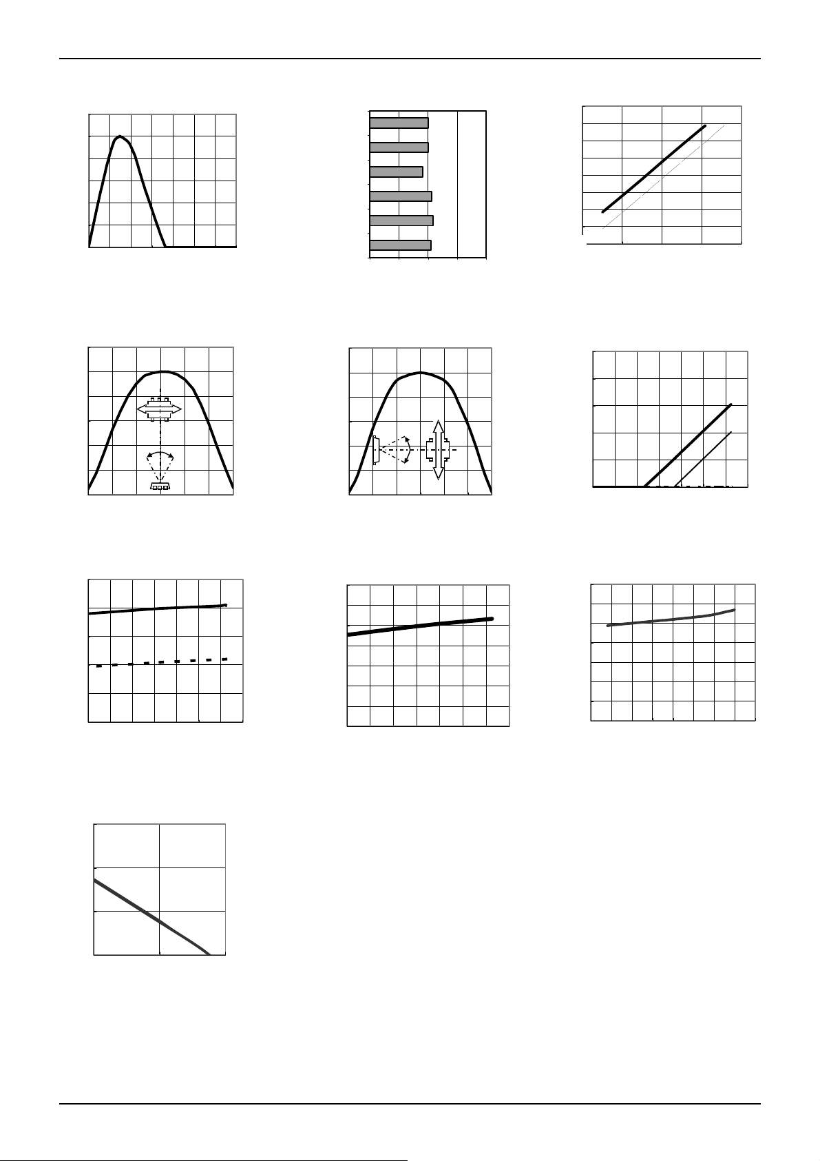
●Reference Data
1.2
1.0
0.8
0.6
Ratio
0.4
0.2
0.0
400 500 600 700 800 900 1000 1100
Wave length [ nm ]
Fig.1 Spectral Response
1.2
1
0.8
受信指向角特性
0.6
Ratio
0.4
0.2
0
-90 -60 -30 0 30 60 90
1pin
-
Angle [ deg ]
+
Fluorescent
Light
Incandescent
Light
Halogen Light
Kripton Light
Artifical Sun
Light
White LED
00.511.52
Ratio
Fig.2 Light Source Dependency
( Fluorescent Light is set to '1' )
1.2
1
0.8
暗電流温特
0.6
Ratio
0.4
0.2
0
-90 -60 -30 0 30 60 90
Angle [ deg ]
-
1pin
+
100000
10000
1000
100
10
1
IOUT [ uA ]
0.1
0.01
0.01
0.001
0 1 100 10,000 1,000,000
H-Gain
照度
[ lx ]
Fig.3 Illuminance - IOUT
Characteristics
100
10
1
0.1
IOUT [ uA ]
0.01
0.001
-40 -20 0 20 40 60 80 100
Ta [ ℃ ]
Fig.4 Directional Characteristics 1 Fig.5 Directional Characteristics 2 Fig.6 Ta – IOUT ( 0 lx )
L-Gain
H-Gain
L-Gain
SD
100
10
1
0.1
ICC [ uA ]
0.01
0.001
-40-200 20406080100
Ta [ ℃ ]
Fig.7 Ta – ICC ( 0 lx )
1000
100
10
WakeupTime [ us ]
1
100 1000 10000
L-Gain
H-Gain
Illuminance [ lx ]
H-Gain
L-Gain
SD
1.4
1.2
1
0.8
Ratio
0.6
0.4
0.2
0
-40 -20 0 20 40 60 80 100
Ta [ ℃ ]
Fig.8 IOUT Temperature dependency
( 100 lx )
1.4
1.2
1.0
0.8
0.6
Ratio
0.4
0.2
0.0
2 2.5 3 3.5 4 4.5 5 5.5 6
VCC [ V ]
Fig.9 IOUT VCC dependency
Fig.10 Illuminance – Wake up Time
www.rohm.com
© 2012 ROHM Co., Ltd. All rights reserved.
3/9
2012.02 - Rev.D

BH1621FVC
●Block Diagram
●Block Diagram Descriptions
・PD
QPhoto diode close to human eyes sensitivity.
・Current AMP
To amplify Photo diode current ( H-Gain / L-Gain )
Gain controllable in 2 steps by input voltage from GC1 and GC2.
・Logic
Logic block for mode setting by input voltage from GC1 and GC2
●Mode Setting
GC2 GC1 Mode
0 0 Shutdown
0 1 H-Gain Mode
1 0 L-Gain Mode
1 1 Shutdown
PD
VCC
Current
Amp
GND
Logic
GC1
GC2
IOUT
R1
Technical Note
C1
www.rohm.com
© 2012 ROHM Co., Ltd. All rights reserved.
4/9
2012.02 - Rev.D

BH1621FVC
Technical Note
●External parts Setting
1) Gain setting of BH1621FVC
Please select the best gain controlled by 3 and 4pin based on the required illuminance range.
The reference is as follows.
Illuminance detection range [lx] Gain Mode
~1000 H-Gain Mode
~50,000 L-Gain Mode
This device will be mounted under the optical window in actual designing. Therefore, there is a possibility that the
illuminace to ALS ( Ambient Light Sensor ) will be less than the illuminance on the final product surface.
Please consider the attenuation of light through the optical window.
It is possible to detect illuminance up to about 5000 lx even in the H-Gain mode. However, the maximum output current
is about 3mA in this case. If you want to minimize consumption current, please use the L-Gain mode as much as possible.
Please set output resistance value ( R1 ) within the range of 1 kΩ ~ 1MΩ which needs to be smaller than the input
impedance of the next circuit.
2) Approximate formula of IOUT output voltage in each Gain Mode
(1) H-Gain mode
The output voltage is calculated as below.
Viout= 0.60 x 10
Viout is IOUT output voltage [V]. Ev is an illuminance of the ALS surface [lx].
R1 is IOUT output resistor[Ω].
( For example ) In case you want to convert the illuminance value up to 500 lx by ADC.
If the maximum voltage of ADC input is 2V, output resistor value will be as below.
R1 = Viout/(0.60 x 10
= 2 /(0.60 x 10-6 x 500) = 6667[Ω]
⇒6.8[kΩ]
(2) L-Gain mode
Viout= 0.063 x 10
3) C1
(1) To reject the flicker light..
In case IOUT output is R1 only and an ALS receives the artificial lights such as fluorescent lamps and incandescent
lamps synchronized with 50/60 Hz of AC power supplies, the output current has a ripple. If you want to reject this ripple,
please add C1 to R1 in parallel. Please set it to C1 x R1 = about 0.1 as a time constant.
(2) To control backlight smoothly by using illuminance value.
C1 is effective to control backlight smoothly for a rapid changing of the illuminance. In this case, please set it to C1 x R1
= about 1 ~ 10 as a time constant. It is not necessary if you average illuminance value with software to change backlight
smoothly.
Please note that the rise time becomes slow at power-on and recovery from shutdown mode to operation mode.
-6
x Ev x R1
-6
x Ev x R1
-6
x Ev)
www.rohm.com
© 2012 ROHM Co., Ltd. All rights reserved.
5/9
2012.02 - Rev.D

BH1621FVC
●Terminal Descriptions
PIN No. Terminal Name Equivalent Circuit Function
Technical Note
1 VCC
2 GND
3 GC1
4 GC2
Power Supply Terminal
GND Terminal
VCC
Mode Setting Terminal 1
VCC
Mode Setting Terminal 2
VCC
This terminal outputs current depending on
5 IOUT
illuminance level.
Use this pin by putting resistor between
GND.
www.rohm.com
© 2012 ROHM Co., Ltd. All rights reserved.
6/9
2012.02 - Rev.D

BH1621FVC
A
●Package Outlines
●Optical design for the device
Production
Code
Min.0.4 mm
Min.0.4 mm
C
0.8 mm
Min.0.4 mm
Technical Note
Lot No.
WSOF5 ( Unit : mm )
0.6 mm
Min.0.4 mm
PD area ( 0.25 mm x 0.3 mm )
Please design an optical window to have the focused
light within this area.
www.rohm.com
© 2012 ROHM Co., Ltd. All rights reserved.
7/9
2012.02 - Rev.D

BH1621FVC
●Cautions on use
1) Absolute Maximum Ratings
An excess in the absolute maximum ratings, such as supply voltage ( Vmax ), temperature range of operating conditions
( Topr ), etc., can break down devices, thus making impossible to identify breaking mode such as a short circuit or an open
circuit. If any special mode exceeding the absolute maximum ratings is assumed, consideration should be given to take
physical safety measures including the use of fuses, etc.
2) GND voltage
Make setting of the potential of the GND terminal so that it will be maintained at the minimum in any operating state.
Furthermore, check to be sure no terminals are at a potential lower than the GND voltage including an actual electric
transient.
3) Short circuit between terminals and erroneous mounting
In order to mount ICs on a set PCB, pay thorough attention to the direction and offset of the ICs. Erroneous mounting can
break down the ICs. Furthermore, if a short circuit occurs due to foreign matters entering between terminals or between
the terminal and the power supply or the GND terminal, the ICs can break down.
4) Operation in strong electromagnetic field
Be noted that using ICs in the strong electromagnetic field can malfunction them.
5) Inspection with set PCB
On the inspection with the set PCB, if a capacitor is connected to a low-impedance IC terminal, the IC can suffer stress.
Therefore, be sure to discharge from the set PCB by each process. Furthermore, in order to mount or dismount the set
PCB to/from the jig for the inspection process, be sure to turn OFF the power supply and then mount the set PCB to the jig.
After the completion of the inspection, be sure to turn OFF the power supply and then dismount it from the jig. In addition,
for protection against static electricity, establish a ground for the assembly process and pay thorough attention to the
transportation and the storage of the set PCB.
6) Input terminals
In terms of the construction of IC, parasitic elements are inevitably formed in relation to potential. The operation of the
parasitic element can cause interference with circuit operation, thus resulting in a malfunction and then breakdown of the
input terminal. Therefore, pay thorough attention not to handle the input terminals; such as to apply to the input terminals a
voltage lower than the GND respectively, so that any parasitic element will operate. Furthermore, do not apply a voltage to
the input terminals when no power supply voltage is applied to the IC. In addition, even if the power supply voltage is
applied, apply to the input terminals a voltage lower than the power supply voltage or within the guaranteed value of
electrical characteristics.
Technical Note
7) Thermal design
Perform thermal design in which there are adequate margins by taking into account the permissible dissipation (pd) in
actual states of use.
8) Treatment of package
Dusts or scratch on the photo detector may affect the optical characteristics. Please handle it with care.
9) Rush current
When power is first supplied to this IC, rush current may flow instantaneously. Because it is possible that the charge
current to the parasitic capacitance of internal photo diode or the internal logic may be unstable. Therefore, give special
consideration to power coupling capacitance, power wiring, width of GND wiring, and routing of connections.
10) The exposed central pad on the back side of the package
There is an exposed central pad on the back side of the package. Please mount by footprint dimensions described in the
Jisso Information for WSOF5. This pad is GND pin, therefore there is a possibility that LSI malfunctions and heavy-current
is generated.
www.rohm.com
© 2012 ROHM Co., Ltd. All rights reserved.
8/9
2012.02 - Rev.D

BH1621FVC
●Ordering part number
B H 1 6 2 1 F V C - T R
Part No. Part No.
WSOF5
1.6±0.05
0.6MAX
1.2±0.05
+0.03
0.02
(MAX 1.28 include BURR)
–0.02
1.6±0.05
(0.05)
0.5
1.0±0.05
5
4
321
(0.91)
S
0.1 S
0.22±0.05
(0.41)
(0.8)
(0.3)
45
1
32
0.08
0.2MAX
0.13±0.05
M
(Unit : mm)
Package
FVC: WSOF5
<Tape and Reel information>
Embossed carrier tapeTape
Quantity
Direction
of feed
3000pcs
TR
The direction is the 1pin of product is at the upper right when you hold
()
reel on the left hand and you pull out the tape on the right hand
Reel
Packaging and forming specification
TR: Embossed tape and reel
Order quantity needs to be multiple of the minimum quantity.
∗
Technical Note
1pin
Direction of feed
www.rohm.com
© 2012 ROHM Co., Ltd. All rights reserved.
9/9
2012.02 - Rev.D

Notes
No copying or reproduction of this document, in part or in whole, is permitted without the
consent of ROHM Co.,Ltd.
The content specied herein is subject to change for improvement without notice.
The content specied herein is for the purpose of introducing ROHM's products (hereinafter
"Products"). If you wish to use any such Product, please be sure to refer to the specications,
which can be obtained from ROHM upon request.
Examples of application circuits, circuit constants and any other information contained herein
illustrate the standard usage and operations of the Products. The peripheral conditions must
be taken into account when designing circuits for mass production.
Great care was taken in ensuring the accuracy of the information specied in this document.
However, should you incur any damage arising from any inaccuracy or misprint of such
information, ROHM shall bear no responsibility for such damage.
The technical information specied herein is intended only to show the typical functions of and
examples of application circuits for the Products. ROHM does not grant you, explicitly or
implicitly, any license to use or exercise intellectual property or other rights held by ROHM and
other parties. ROHM shall bear no responsibility whatsoever for any dispute arising from the
use of such technical information.
The Products specied in this document are intended to be used with general-use electronic
equipment or devices (such as audio visual equipment, ofce-automation equipment, communication devices, electronic appliances and amusement devices).
The Products specied in this document are not designed to be radiation tolerant.
While ROHM always makes efforts to enhance the quality and reliability of its Products, a
Product may fail or malfunction for a variety of reasons.
Please be sure to implement in your equipment using the Products safety measures to guard
against the possibility of physical injury, re or any other damage caused in the event of the
failure of any Product, such as derating, redundancy, re control and fail-safe designs. ROHM
shall bear no responsibility whatsoever for your use of any Product outside of the prescribed
scope or not in accordance with the instruction manual.
The Products are not designed or manufactured to be used with any equipment, device or
system which requires an extremely high level of reliability the failure or malfunction of which
may result in a direct threat to human life or create a risk of human injur y (such as a medical
instrument, transportation equipment, aerospace machinery, nuclear-reactor controller, fuelcontroller or other safety device). ROHM shall bear no responsibility in any way for use of any
of the Products for the above special purposes. If a Product is intended to be used for any
such special purpose, please contact a ROHM sales representative before purchasing.
If you intend to export or ship overseas any Product or technology specied herein that may
be controlled under the Foreign Exchange and the Foreign Trade Law, you will be required to
obtain a license or permit under the Law.
Notice
www.rohm.com
© 2012 ROHM Co., Ltd. All rights reserved.
Thank you for your accessing to ROHM product informations.
More detail product informations and catalogs are available, please contact us.
ROHM Customer Support System
http://www.rohm.com/contact/
R1120
A
 Loading...