

Page 1
Parameter
Symbol
Limit
Unit
Conditions
MIN
TYP
MAX
Supply Voltage
BD9G1010G
VCC 6 -
42
V
Output Voltage / Current
BD9G101G
VOUT - 5 - V
*Set by R1 and R2
BD9G101G
IOUT - 0.5 - A
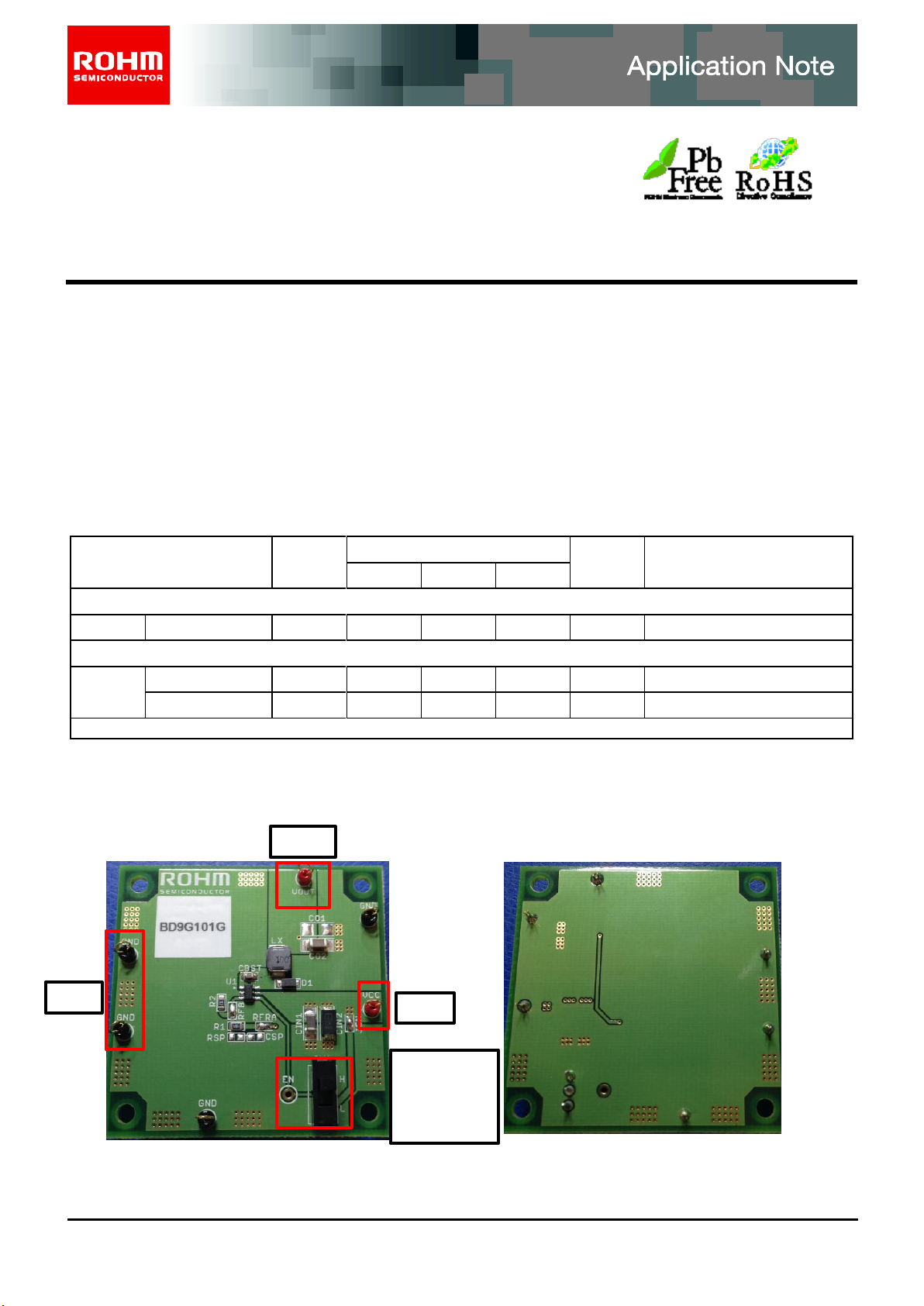
No.0000000015
BD9673EFJ Eval Board
BD9G101G Eval Board (Back)
GND
Vout
BD9G101G Eval Board (Front)
EN
VOUT
VCC
GND
ENABLE
H: Active
(ICOFF)
L: Inactive
(ICON)
ROHM Switching Regulator Solutions
Evaluation Board:
Step-down Switching Regulator
With Built-in Power MOSFET
BD9G101G (5V | 0.5A Output)
●Introduction
This application note will provide the steps necessary to operate and evaluate ROHM’s step-down switching regulator using the BD9G101G
evaluation boards. Board layout recommendations, operation procedures, application data and build of materials are provided.
●Description
This evaluation board has been developed for ROHM’s step-down switching regulator customers evaluating BD9G101G. While accepting a
wide power supply of 6-42V, a step down output of 1V-29V can be produced. The IC has an internal 800mohm Nch MOSFET (1A max) and
a fixed operating frequency range of 1.5MHz. A Soft Start circuit prevents in-rush current during startup along with UVLO (low voltage error
prevention circuit), OCP (over-current protection) and TSD (thermal shutdown detection) protection circuits. An EN pin allows for simple
ON/OFF control of the IC to reduce standby current consumption.
●Applications
Industrial distributed power applications
Automotive and battery powered equipment
●Evaluation Board Operating Limits and Absolute Maximum Ratings
●Evaluation Board
Below is the evaluation board with the BD9G101G. Component selection and board layout guidelines are provided in the
BD9G101G datasheet.
1
Page 2
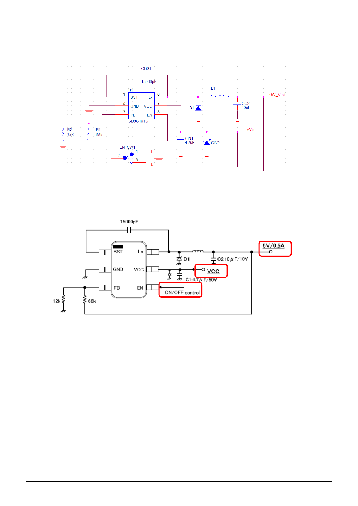
Application Note
L1: 10uH
10uH
●Evaluation Board Schematic
Below is the evaluation board schematic for BD9G101G.
●Evaluation Board I/O
Below is the reference application circuit that shows the inputs (Vcc and EN) and the output (Vout @ 5V/0.5A)
●Evaluation Board Operation Procedures
Below is the procedure to operate the evaluation board
1. Connect GND to a GND pin on the evaluation board
2. Connect Vcc to the VCC_pin. This will provide Vcc to the Vcc pin of the IC
i. Note: EN pin is pulled HIGH as default. EN needs to be set to LOW for IC operation.
3. Output voltage can be measured from the VOUT_pin on the evaluation board. Output current can be measured with a
proper load at VOUT.
Page 2 of 8
Page 3
Application Note
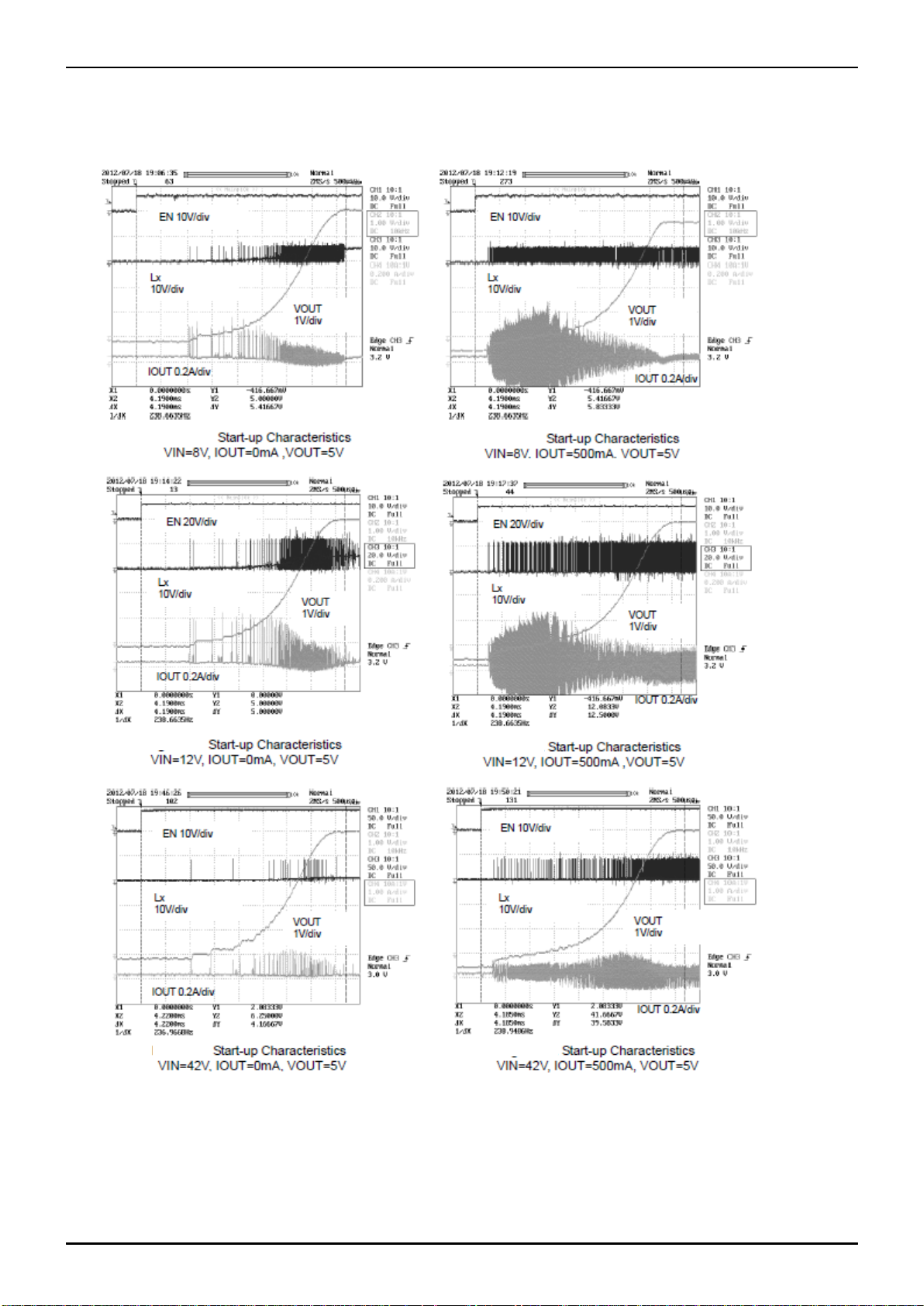
●Reference Graphs Application Data for BD9G101G
Below graphs show efficiency, frequency response and load characteristics of the BD9G101G eval board.
Page 3 of 8
Page 4

Application Note
Page 4 of 8
Page 5

Application Note
Page 5 of 8
Page 6

Application Note
Note: Feed-forward capacitor Csp is not populated on the BD9G101G evaluation board. The capacitor is recommended
for designs requiring improved phase margin and transient response.
●Evaluation Board Layout Guidelines
Below are the guidelines that have been followed and recommended for BD9G101G designs.
Page 6 of 8
Page 7

Application Note
Item
Qty
Ref
Description
Manufacturer
Part Number
Digikey P/N
1 1 CIN1
CAP CER 4.7UF 50V Y5V 1206
Murata
GRM31CF51H475ZA01L
490-1828-1-ND
2
1
CIN2
DIODE TVS 30V 400W UNI 5%
SMA
Littlefuse
SMAJ30A
SMAJ30ALFTR-ND
3 1 CO2
CAP CER 10UF 10V 10% X5R
1206
Murata
GRM31CR61A106KA01L
490-1820-2-ND
4 1 CBST
CAP CER 0.015UF 50V 10% X7R
0603
Murata
GRM188R71H153KA01D
490-1514-1-ND
5 1 D1
DIODE SCHOTTKY 60V 2A PMDU
ROHM
RB060M-60TR
RB060M-60CT-ND
6 1 SW1
SWITCH SLIDE SPDT 30V.2A PC
MNT
E-Switch
EG1218
EG1903-ND
7 1 R1
RES 68.0K OHM 1/8W 1% 0805
SMD
Yageo
RC0805FR-0768KL
311-68.0KCRCT-ND
8 1 R2
RES 12.0K OHM 1/8W 1% 0805
SMD
Yageo
RC0805FR-0712KL
311-12.0KCRCT-ND
9 1 LX
INDUCT 10uH SOD-106
TOKO
DEM4518C
1235AS-H-100M
-
10 1 U1
5V, 0.5A Step-down SW Reg w/
FET
ROHM
BD9G101G
-
●Evaluation Board BOM
Below is a table with the build of materials. Part numbers and supplier references are provided.
Page 7 of 8
Page 8

Application Note
Page 8 of 8
 Loading...