

Page 1
Switching Regulator Series
Step-Down DC/DC Converter
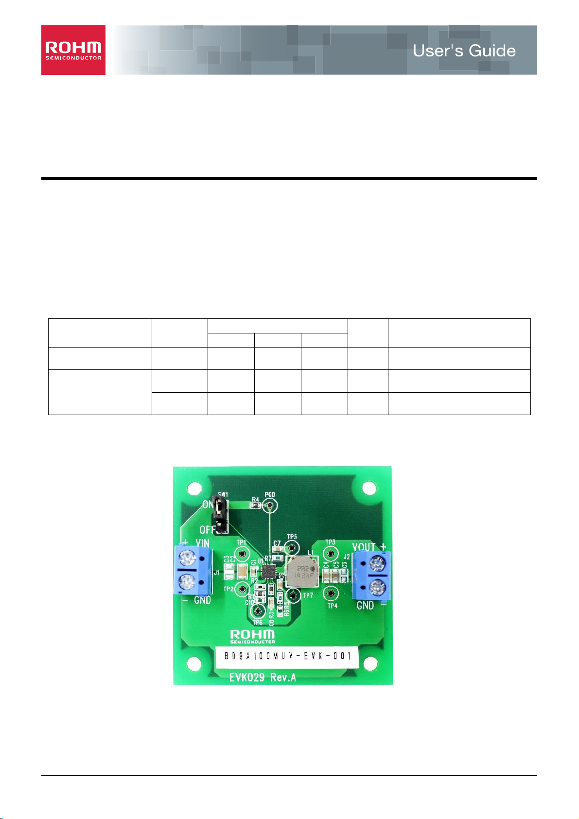
BD9A100MUV Evaluation Board
BD9A100MUV-EVK-001
Description
This evaluation board has been developed for ROHM’s synchronous buck DC/DC converter customers evaluating
BD9A100MUV. While accepting a power supply of 2.7-5.5V, an output of 1.8V can be produced. The IC has internal 60m
high-side N-channel MOSFET and 60m low-side N-channel MOSFET and a synchronization frequency is of 1MHz. A
Soft Start circuit prevents in-rush current during startup. An EN pin allows for simple ON/OFF control of the IC to reduce
standby current consumption. A MODE pin allows the user to select fixed frequency PWM mode or enables the Deep-SLLM
control and the mode is automatically switched between the Deep-SLLM control and fixed frequency PWM mode. Include
OCP (Over Current Protection) and SCP (Short Circuit Protection).
Evaluation Board Operating Limits and Absolute Maximum Ratings (Ta=25℃)
Parameter Symbol
MIN TYP MAX
Limit
Unit Conditions
Supply Voltage VCC 2.7 - 5.5 V
Output Voltage /
Current
Evaluation Board
- 1.8 - V
V
OUT
I
- - 1 A
OUT
Figure 1. BD9A100MUV-EVK-001 Evaluation Board
www.rohm.co.jp
© 2015 ROHM Co., Ltd. All rights reserved.
1/9
9 September 2015 Rev.002
Page 2
BD9A100MUV-EVK-001
V
+
-
+
-
+
DC Voltmeter 2
V
-
+
Load
-
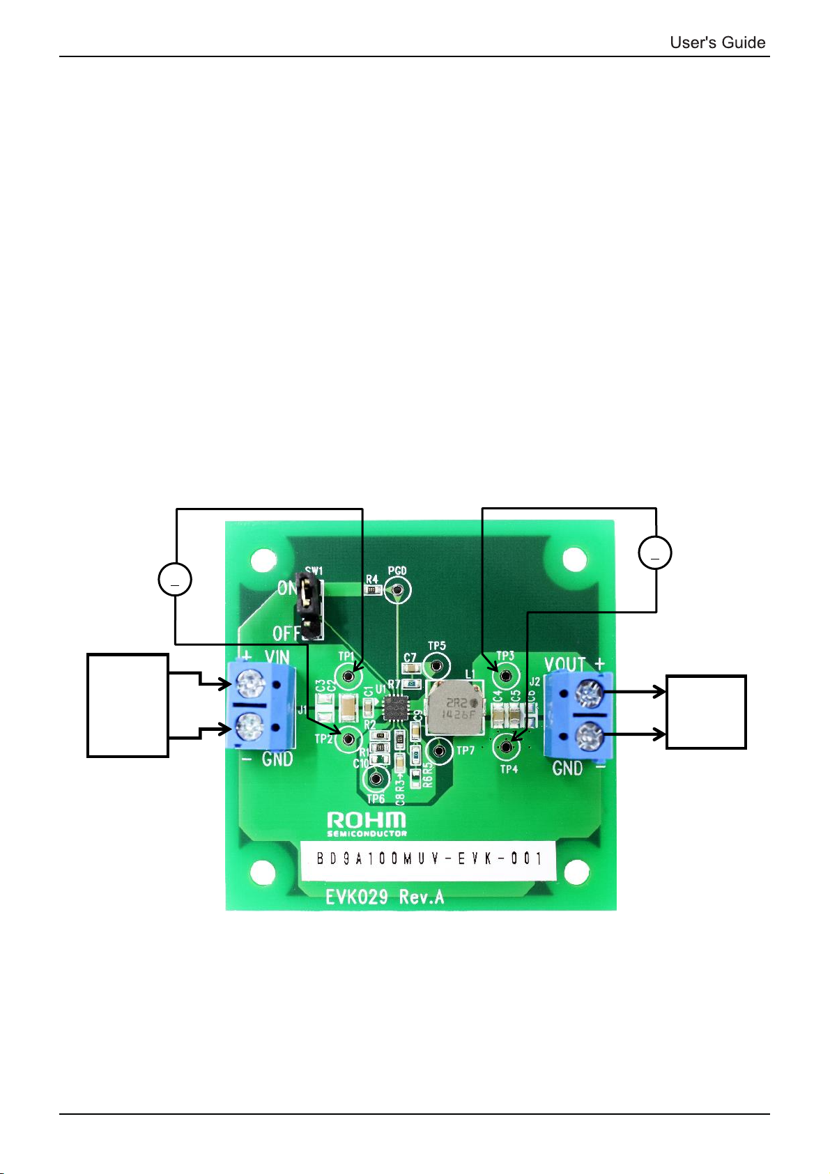
Figure 2. Connection Diagram
Operation Procedures
1. Necessary equipments
(1) DC power-supply of 2.7V to 5.5V/1A
(2) Maximum 1A load
(3) DC voltmeter
2. Connecting the equipments
(1) DC power-supply presets to 5.0V and then the power output turns off.
(2) The max. load should be set at 1A and over it will be disabled.
(3) Check Jumper pin of SW1 is short, between intermediate-terminal and OFF-side terminal.
(4) Connect positive-terminal of power-supply to VIN+terminal and negative-terminal to GND-terminal with a pair of wires.
(5) Connect load’s positive-terminal to VOUT+terminal and negative-terminal to GND-terminal with a pair of wires.
(6) Connect positive-terminal of DC voltmeter 1 to TP1 and negative-terminal to TP2 for input-voltage measurement.
(7) Connect positive-terminal of DC voltmeter 2 to TP3 and negative-terminal to TP4 for output-voltage measurement.
(8) DC power-supply output is turned ON.
(9) IC is enable (EN) by shorting Jumper-pin of SW1 between intermediate-terminal and ON-side terminal.
(10) Check DC voltmeter 2 displays 1.8V.
(11) The load is enabled.
(12) Check at DC voltmeter 1 whether the voltage-drop (loss) is not caused by the wire’s resistance.
DC Voltmeter 1
DC Power
Enable-Pin
To minimize current consumption during standby-mode and normal operation, Enable-mode can be switched by controlling
EN pin(15pin) of the IC. Standby-mode is enabled by shorting Jumper-pin of SW1 between intermediate-terminal and
OFF-side terminal and normal-mode operation by shorting between intermediate-terminal and ON-side terminal.
It also can be swithed between standby-mode and normal-mode operation by removing Jumper-pin and controlling the
voltage between EN and GND-terminal. Standby-mode is enabled when the voltage of EN is under 0.5V, and normal-mode
operation when it is over 2.0V.
www.rohm.co.jp
© 2015 ROHM Co., Ltd. All rights reserved.
2/9
9 September 2015 Rev.002
Page 3
A
A
BD9A100MUV-EVK-001
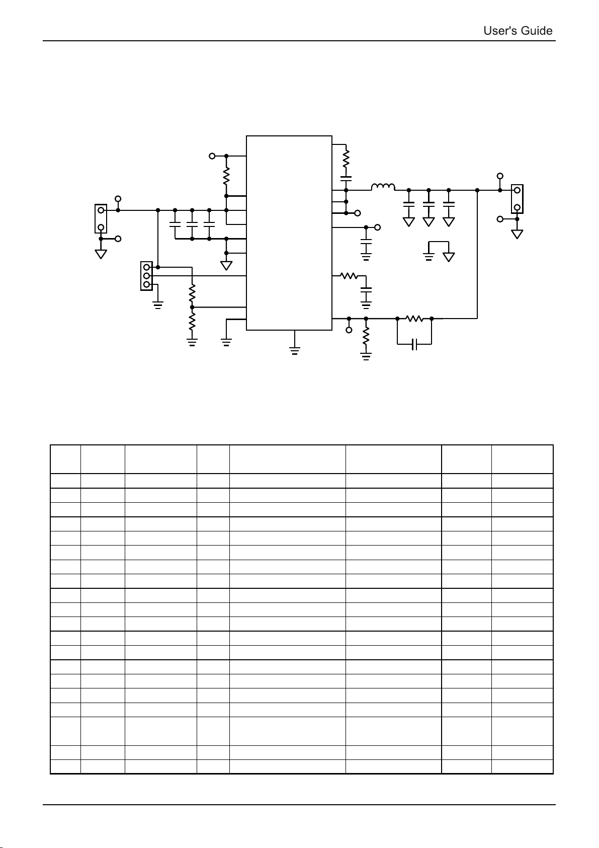
Cricuit Diagram
= 2.7V~5.5V, V
V
IN
OUT
= 1.8V
BD9
U1
100MUV
VIN
BOOT 13
SW 12
SW 11
SW 10
SS 9
ITH 7
D
A
P
E
FB 6
7
1
R3
TP6
R7
C7
TP5
C9
C8
R2
L1
TP7
TP3
C4 C 5 C6
TP4
R1
C10
P G D
14 PGD
C1 C 2 C3
R5
R6
R 4
16
1PVIN
2PVIN
3PGND
4PGND
15 EN
8MODE
5AGND
VIN
G N D
J1
TP 1
TP2
O FF
S W1
ON
Figure 3. BD9A100MUV-EVK-001 Circuit Diagram
Bill of Materials
Reference
Count
Designator
2 C1, C7 Ceramic Capacitor 0.1µF 50V, B, ±10% GRM188B31H104KA92D MURATA 1608
1 C2 Ceramic Capacitor 10µF 16V, B, ±10% GRM31CB31C106KA88L MURATA 3216
0 C3 Ceramic Capacitor - Not installed - - 3216
2 C4, C5 Ceramic Capacitor 22µF 6.3V, B, ±20% GRM21BB30J226ME38L MURATA 2012
0 C6 Ceramic Capacitor - Not installed - - 2012
1 C8 Ceramic Capacitor 2700pF 50V, B, ±10% GRM188B11H272KA01D MURATA 1608
1 C9 Ceramic Capacitor 0.01µF 50V, B, ±10% GRM188B11H103KA01D MURATA 1608
0 C10 Ceramic Capacitor - Not installed - - 1608
1 L1 Inductor 2.2µH ±20%, DCR=17mmax, 8.1A FDSD0630-H-2R2M TOKO 7066
1 R1 Resis tor 30k 1/10W, 50V, ±1% MCR03EZPF3002 ROHM 1608
1 R2 Resis tor 24k 1/10W, 50V, ±1% MCR03EZPF2402 ROHM 1608
1 R3 Res istor 9.1k 1/10W, 50V, ±1% MCR03EZPF9101 ROHM 1608
1 R4 Resis tor 10k 1/10W, 50V, ±1% MCR03EZPF1002 ROHM 1608
2 R5, R7 Resistor 0 Jumper MCR03EZPJ000 ROHM 1608
0 R6 Resis tor - Not installed - - 1608
1 SW1 Pin header - 2.54mm × 3 contacts PH-1x03SG USECONN -
1 U1 IC - Buck DC/DC Converter BD9A100MUV ROHM VQFN016V3030
2 J1, J2 Terminal Block - 2 contacts, 15A, 14 to 22AWG TB111-2-2-U-1-1
1 - Jumper - Jumper pin for SW1 MJ254-6BK USECONN -
1 - PCB - FR4, 4-layer, 1oz EVK029 Rev.A Tamukai 50×50×1.6
Type Value Description
Manufacturer
Part Number
Manufacturer
Alphaplus
Connectors
& Cables
J2
VOUT
GND
Configuration
(mm )
-
www.rohm.co.jp
© 2015 ROHM Co., Ltd. All rights reserved.
3/9
9 September 2015 Rev.002
Page 4

BD9A100MUV-EVK-001
Layout (PCB size: 50mm×50mm×1.6mm)
Figure 4. Top Silk Screen (Top view)
Figure 5. Top Silk Screen and Layout (Top view)
www.rohm.co.jp
© 2015 ROHM Co., Ltd. All rights reserved.
4/9
9 September 2015 Rev.002
Page 5

BD9A100MUV-EVK-001
Figure 6. Top Side Layout (Top view)
Figure 7. L2 Layout (Top view)
www.rohm.co.jp
© 2015 ROHM Co., Ltd. All rights reserved.
5/9
9 September 2015 Rev.002
Page 6

BD9A100MUV-EVK-001
Figure 8. L3 Layout (Top view)
Figure 9. Bottom Side Layout (Top view)
www.rohm.co.jp
© 2015 ROHM Co., Ltd. All rights reserved.
6/9
9 September 2015 Rev.002
Page 7

BD9A100MUV-EVK-001
9 September 2015 Rev.002
© 2015 ROHM Co., Ltd. All rights reserved.
www.rohm.co.jp
0
10
20
30
40
50
60
70
80
90
100
0.001 0.01 0.1 1
Efficiency (%)
Load Current (A)
VIN=3.3V
VIN=5.0V
-0.4
-0.3
-0.2
-0.1
0
0.1
0.2
0.3
0.4
2 2.5 3 3.5 4 4.5 5 5.5 6
Output Voltage Change (%)
Input Voltage (V)
-0.5
-0.4
-0.3
-0.2
-0.1
0
0.1
0.2
0.3
0.4
0.5
0 0.2 0.4 0.6 0.8 1
Output Voltage Change (%)
Load Current (A)
VIN=5.0V
Figure 10. Efficiency vs Load Current
Figure 11. Line Regulation
Figure 12. Load Regulation
Figure 13. Load Transient Characteristics
VO (AC)
50mV/div
IO: 0.5A/div
V
IN
= 5.0V
VO = 1.8V
IO: 0A→1A→0A
Time scale 1ms/div
VO=1.8V
VO=1.8V
7/9
Page 8

BD9A100MUV-EVK-001
9 September 2015 Rev.002
© 2015 ROHM Co., Ltd. All rights reserved.
www.rohm.co.jp
-180
-135
-90
-45
0
45
90
135
180
-80
-60
-40
-20
0
20
40
60
80
1000 10K 100K 1M
Phase (deg)
Gain (dB)
Frequency (Hz)
Figure 14. Loop Response VIN = 5.0V, VO = 1.8V, IO = 1.0A
Phase
Gain
Figure 15. Input Voltage Ripple Wave
VIN = 5.0V, VO = 1.8V, IO=0A
Figure 16. Input Voltage Ripple Wave
VIN = 5.0V, VO = 1.8V, IO=1A
V
IN
(AC)
50mV/div
Time scale 20ms/div
VSW
2V/div
Time scale 1μs/div
V
IN
(AC)
50mV/div
VSW
2V/div
8/9
Page 9

BD9A100MUV-EVK-001
9 September 2015 Rev.002
© 2015 ROHM Co., Ltd. All rights reserved.
www.rohm.co.jp
Time scale 2ms/div
VO (AC)
20mV/div
VSW
2V/div
Figure 17. Output Voltage Ripple Wave
VIN = 5.0V, VO = 1.8V, IO=0A
Time scale 1μs/div
V
IN
5V/div
EN
5V/div
VO
1V/div
Time scale 1ms/div
Time scale 1ms/div
Figure 19. Start-up by EN
VIN = 5.0V, VO = 1.8V
Figure 20. Power-down by EN
VIN = 5.0V, VO = 1.8V
Figure 18. Output Voltage Ripple Wave
VIN = 5.0V, VO = 1.8V, IO=1A
VO (AC)
20mV/div
VSW
2V/div
V
SW
5V/div
9/9
Page 10

Notes
1)
The information contained herein is subject to change without notice.
2)
Before you use our Products, please contact our sales representative and verify the latest specifications :
3)
Although ROHM is continuously working to improve product reliability and quality, semiconductors can break down and malfunction due to various factors.
Therefore, in order to prevent personal injury or fire arising from failure, please take safety
measures such as complying with the derating characteristics, implementing redundant and
fire prevention designs, and utilizing backups and fail-safe procedures. ROHM shall have no
responsibility for any damages arising out of the use of our Poducts beyond the rating specified by
ROHM.
4)
Examples of application circuits, circuit constants and any other information contained herein are
provided only to illustrate the standard usage and operations of the Products. The peripheral
conditions must be taken into account when designing circuits for mass production.
5)
The technical information specified herein is intended only to show the typical functions of and
examples of application circuits for the Products. ROHM does not grant you, explicitly or implicitly,
any license to use or exercise intellectual property or other rights held by ROHM or any other
parties. ROHM shall have no responsibility whatsoever for any dispute arising out of the use of
such technical information.
6)
The Products are intended for use in general electronic equipment (i.e. AV/OA devices, communication, consumer systems, gaming/entertainment sets) as well as the applications indicated in
this document.
7)
The Products specified in this document are not designed to be radiation tolerant.
8)
For use of our Products in applications requiring a high degree of reliability (as exemplified
below), please contact and consult with a ROHM representative : transportation equipment (i.e.
cars, ships, trains), primary communication equipment, traffic lights, fire/crime prevention, safety
equipment, medical systems, servers, solar cells, and power transmission systems.
9)
Do not use our Products in applications requiring extremely high reliability, such as aerospace
equipment, nuclear power control systems, and submarine repeaters.
10)
ROHM shall have no responsibility for any damages or injury arising from non-compliance with
the recommended usage conditions and specifications contained herein.
11)
ROHM has used reasonable care to ensur the accuracy of the information contained in this
document. However, ROHM does not warrants that such information is error-free, and ROHM
shall have no responsibility for any damages arising from any inaccuracy or misprint of such
information.
12)
Please use the Products in accordance with any applicable environmental laws and regulations,
such as the RoHS Directive. For more details, including RoHS compatibility, please contact a
ROHM sales office. ROHM shall have no responsibility for any damages or losses resulting
non-compliance with any applicable laws or regulations.
13)
When providing our Products and technologies contained in this document to other countries,
you must abide by the procedures and provisions stipulated in all applicable export laws and
regulations, including without limitation the US Export Administration Regulations and the Foreign
Exchange and Foreign Trade Act.
14)
This document, in part or in whole, may not be reprinted or reproduced without prior consent of
ROHM.
Notice
Thank you for your accessing to ROHM product informations.
More detail product informations and catalogs are available, please contact us.
ROHM Customer Support System
www.rohm.com
© 2015 ROHM Co., Ltd. All rights reserved.
http://www.rohm.com/contact/
R1102
A
 Loading...