

Page 1
Single-chip Type with Built-in FET Switching Regulator Series
Simple Step-down
Switching Regulator
with Built-in Power MOSFET
BD9870FPS
● Description
The BD9870FPS single-channel step-down switching regulator incorporates a Pch MOSFET capable of PWM operation at
900kHz, enabling use of a smaller coil, as well as circuitry that eliminates the need for external compensation – only a diode,
coil, and ceramic capacitor are required – reducing board size significantly.
●Features
1) Maximum switching current: 1.5A
2) 2. Built-in Pch FET ensures high efficiency
3) Output voltage adjustable via external resistors
4) High switching frequency: 900kHz (fixed)
5) Soft start time: 5ms (fixed)
6) Overcurrent and thermal shutdown protection circuits built in
7) ON/OFF control via STBY pin
8) Ceramic output capacitor compatibility
9) Small surface mount TO252S-5 package
●Applications
TVs, printers, DVD players, projectors, gaming devices, PCs, car audio/navigation systems, ETCs, communication
equipment, AV products, office equipment, industrial devices, and more.
●Absolute Maximum Ratings(Ta=25℃)
Parameter Symbol Ratings Unit
Supply Voltage(VCC-GND) Vcc 36 V
STBY-GND V
OUT-GND V
INV-GND V
Maximum Switching Current Iout 1.5
Power Dissipation Pd 800
Operating Temperature Topr -40 to +85 ℃
Storage Temperature Tstg -55 to +150 ℃
(*1) Do not exceed Pd, ASO, and Tjmax=150℃
(*2) Derated at 6.4mW/°C over Ta=25℃
●Operating Conditions(Ta=-40 to +85℃)
Parameter Symbol
Input Voltage VCC 8.0 35.0 V
Output Voltage Vo 1.0 0.8×(VCC-Io×Ron) V
36 V
STBY
36 V
OUT
5 V
INV
MIN MAX
(*1)
A
(*2)
mW
Limit
No.09027EAT26
Unit
www.rohm.com
© 2009 ROHM Co., Ltd. All rights reserved.
1/11
2009.05 - Rev.A
Page 2
BD9870FPS
Technical Note
●Electrical Characteristics(Unless otherwise noted, Ta=25℃,Vcc=12V,Vo=5V,STBY=3V)
Parameter Symbol
MIN TYP MAX
Limit
Unit Conditions
Output ON Resistance Ron - 1.0 1.5 Ω
Efficiency η 80 88 - % Io=0.5A
Switching Frequency fosc 810 900 990 kHz
Load Regulation ΔVOLOAD - 5 40 mV
Vcc=20V,
Io=0.5 to 1.5A
Line Regulation ΔVOLINE - 5 25 mV Vcc=10 to 30V, Io=1.0A
Over Current ProtectionLimit Iocp 1.6 - - A
INV Pin Threshold Voltage VINV 0.99 1.00 1.01 V
INV Pin Input Current IINV - 1 2 μA VINV=1.0V
STBY Pin Threshold
Voltage
ON VSTBYON 2.0 - 36 V
OFF VSTBYOFF -0.3 - 0.3 V
STBYPin Input Current Istby 5 15 30 μA STBY=3V
Circuit Current Icc - 5 12 mA INV=2V
Stand-by Current Ist - 0 5 μA STBY=0V
Soft Start Time Tss 1 4 10 ms
* This product is not designed to be resistant to radiation.
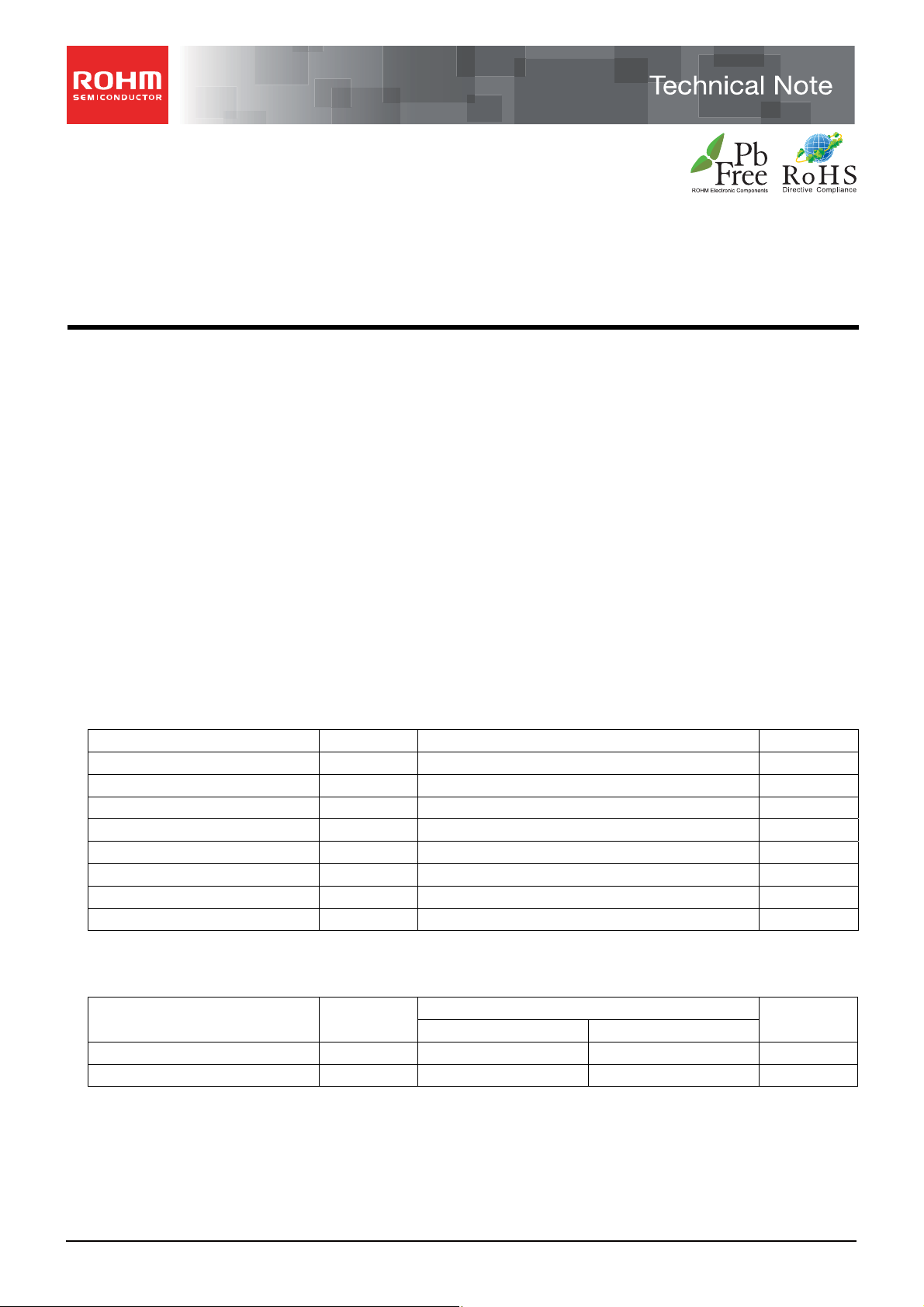
●Block Diagram
VCC
1
VREF
PWM
COMP
DRIVER
STBY
5
OSC
STBY
TSD
CTL
LOGIC
OCP
OUT
2
Error AMP
INV
4
FIN
GND
SS
Fig.1
www.rohm.com
© 2009 ROHM Co., Ltd. All rights reserved.
2/11
2009.05 - Rev.A
Page 3
BD9870FPS
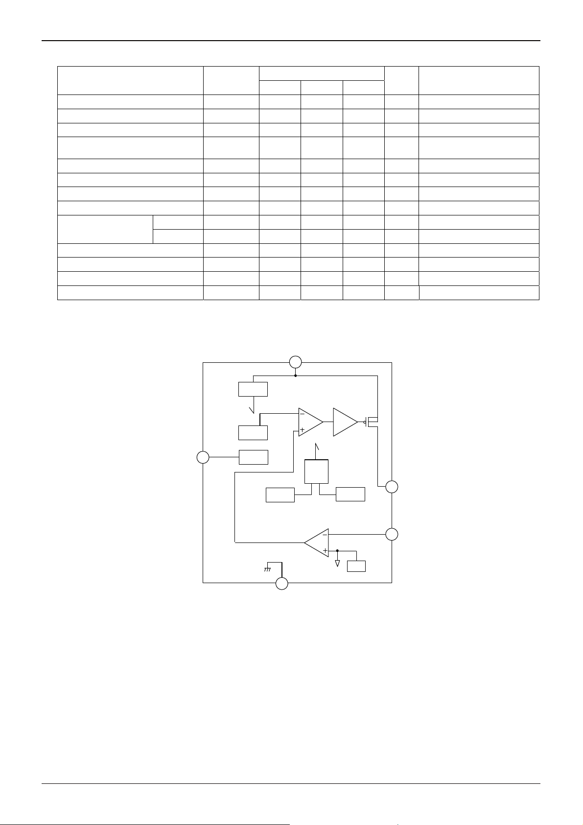
●Package Dimensions
●Pin Description
Pin No. Pin Name Function
1 VCC
2 OUT
3※ OUT
FIN GND
4 INV
5 STBY
※Normally OPEN
Technical Note
TO252S-5(Unit:mm)
Fig.2
Input Power Supply Pin
Internal Pch FET Drain Pin
Internal Pch FET Drain Pin
Ground
Output Voltage Feedback Pin
ON/OFF Control Pin
www.rohm.com
© 2009 ROHM Co., Ltd. All rights reserved.
3/11
2009.05 - Rev.A
Page 4
BD9870FPS
●Block Function Explanations
・ VREF
Generates the regulated voltage from Vcc input, compensated for temperature.
・ OSC
Generates the triangular wave oscillation frequency (900kHz) using an internal resistors and capacitor. Used for PWM
comparator input.
・ Error AMP
This block, via the INV pin, detects the resistor-divided output voltage, compares this with the reference voltage, then
amplifies and outputs the difference.
・ PWM COMP
Outputs PWM signals to the Driver block, which converts the error amp output voltage to PWM form.
・ DRIVER
This push-pull FET driver powers the internal Pch MOSFET, which accepts direct PWM input.
・ STBY
Controls ON/OFF operation via the STBY pin. The output is ON when STBY is High.
・ Thermal Shutdown (TSD)
This circuit protects the IC against thermal runaway and damage due to excessive heat. A thermal sensor detects the
junction temperature and switches the output OFF once the temperature exceeds a threshold value (175°C). Hysteresis is
built in (15°C) in order to prevent malfunctions due to temperature fluctuations.
・ Over Current Protection (OCP)
The OCP circuit detects the voltage difference between Vcc and OUT by measuring the current through the internal Pch
MOSFET and switches the output OFF once the voltage reaches the threshold value. The OCP block is a self-recovery
type (not latch).
・ Soft Start (SS)
This block conducts soft start operations. When STBY is High and the IC starts up the internal capacitor begins charging.
The soft start time is fixed at 5ms.
Technical Note
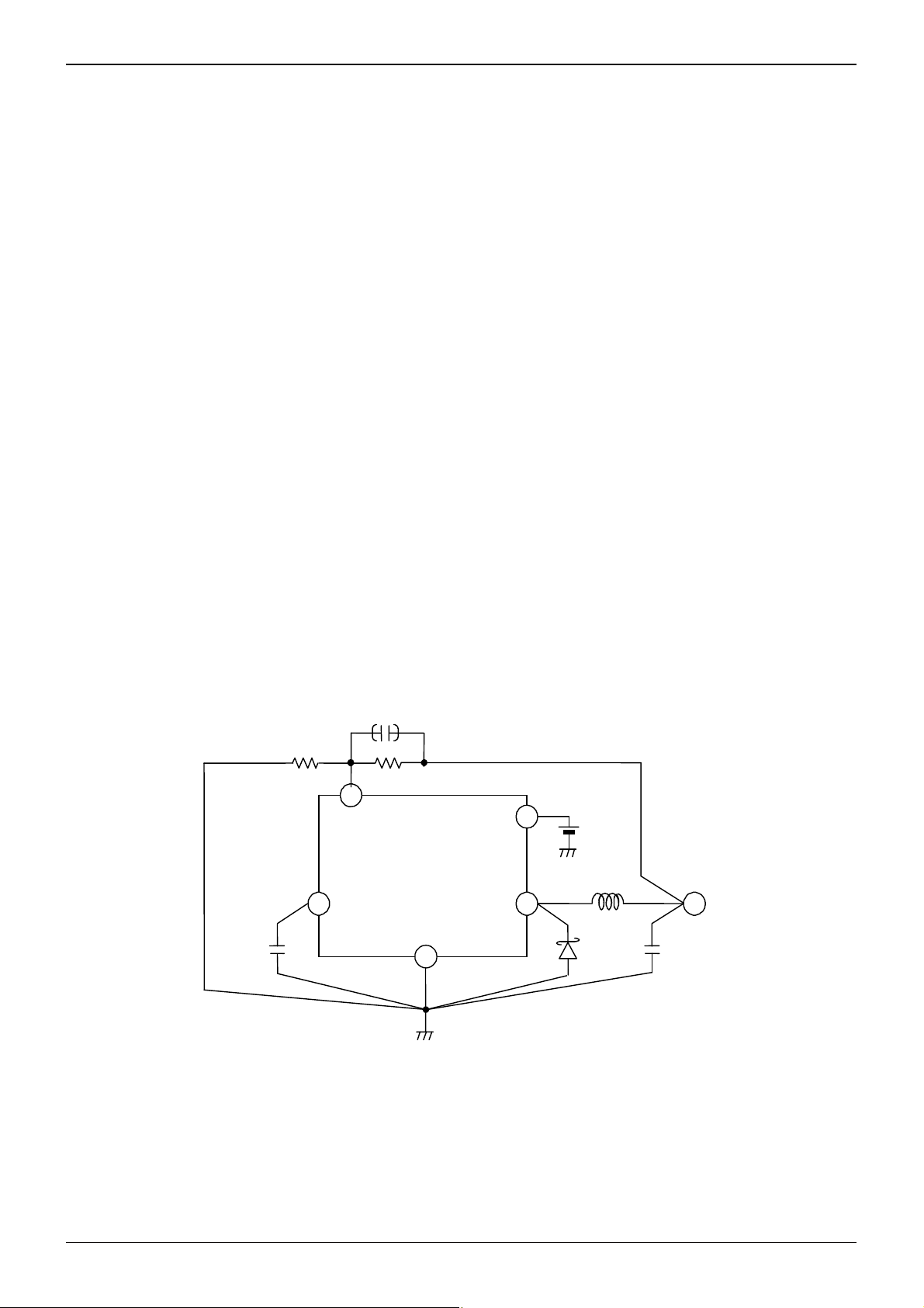
●Notes for PCB layout
• Place capacitors between Vcc and Ground, and the Schottky diode as close as possible to the IC to reduce noise and
maximize efficiency.
• Connect resistors between INV and Ground, and the output capacitor filter at the same Ground potential in order to stabilize
the output voltage.
(If the patterning is longer or thin, it’s possible to cause ringing or waveform crack.)
R2:1kΩ
1
C2
C3
R1:4kΩ
4
INV
VCC OUT
GND
FIN
STBY
Fig.3
5
L1
2
5.0V
C1
D1
www.rohm.com
© 2009 ROHM Co., Ltd. All rights reserved.
4/11
2009.05 - Rev.A
Page 5

BD9870FPS
(
Technical Note
●Application component selection and settings
Inductor L1
A large inductor series impedance will result in deterioration of efficiency. OCP operation greater than 1.6A may cause
inductor overheating, possibly leading to overload or output short.
Note that the current rating for the coil should be higher than I
Iout(MAX): maximum load current
(MAX)+⊿IL.
OUT
If you flow more than maximum current rating, coil will become overload, and cause magnetic saturation, and those
account for
efficiency deterioration. Select from enough current rating of coil which doesn’t over peak current.
⊿IL
VCC-VOUT)
=
L1
×
VOUT
VCC
1
×
fosc
L1:inductor value, VCC:maximum input voltage, VOUT:output voltage,
⊿IL:coil ripple current value, fosc:oscillation frequency
If you make a point of efficiency, we will recommend C10-H5R(mitsumi).The efficiency will improve about 1-2%.
Schottky Diode D1
A Schottky diode with extremely low forward voltage should be used. Selection should be based on the following
guidelines regarding maximum forward current, reverse voltage, and power dissipation:
・The maximum current rating is higher than the combined maximum load current and coil ripple current (⊿I
L
・The reverse voltage rating is higher than the VIN value.
・Power dissipation for the selected diode must be within the rated level.
The power dissipation of the diode is expressed by the following formula:
Pdi=Iout(MAX)×Vf×(1-VOUT/VCC)
Iout(MAX): maximum load current, Vf: forward voltage, VOUT: output voltage, VCC: input voltage
Output Capacitor C1
A suitable output capacitor should satisfy the following formula for ESR:
ESR≦⊿VL/⊿IL
⊿VL : permissible ripple voltage, ⊿IL : coil ripple current
Another factor that must be considered is the permissible ripple current. Select a capacitor with sufficient margin, governed
by the following formula:
IRMS =⊿IL/2√3
IRMS: effective value of ripple current to the output capacitor, ⊿IL : coil ripple current
Use ceramic capacitor over B characteristic of temperature. Except that, it is possible to cause abnormal movement of IC.
It’s depends on ambient temperature or output voltage setting
Also it is possible to use Al electronic capacitor, but use it by enough co nfirmation.
Input Capacitor C2
The input capacitor is the source of current flow to the coil via the built-in Pch FET when the FET is ON. When selecting
the input capacitor sufficient margin must be provided to accommodate capacitor voltage and permissible ripple current.
The expression below defines the effective value of the ripple current to the input capacitor. It should be used in
determining the suitability of the capacitor in providing sufficient margin for the permissible ripple current.
IRMS=IOUT×√
(1-VOUT / VCC)×VOUT / VCC
IRMS : effective value of the ripple current to the input capacitor
IOUT : output load current, VOUT: output voltage, VCC: input voltage
Capacitor C3
This capacitor is utilized to stabilize the freque ncy characteristics, but is seldom used. However, if the phase margin is
insufficient and oscillation is likely, connecting this capacitor may improve frequency stability.
Resistor R1,R2
These resistors determine the output voltage:
VOUT=1.0V×(1 + R1/R2)
Select resistors less than 10kΩ.
).
www.rohm.com
© 2009 ROHM Co., Ltd. All rights reserved.
5/11
2009.05 - Rev.A
Page 6

BD9870FPS
<Recommended Components (Example)>
Inductor L1=10μH :C6-K3LA (MITSUMI)
Schottky Diode D1 :RB050LA-30(ROHM)… use when VCC is less than 30V
D2 :RB050LA-40(ROH M)… use when VCC is greater than 30V
Capacitor C1=10μF(25V) :ceramic cap GRM31CB31E106KA75L(murata)
C2=4.7μF(50V) :ceramic cap GRM32EB31H475KA87L(murata)
C3=OPEN
<Recommended Components example 2>…when the Duty ratio of output/input voltage is less than 10%
Inductor L1=10μH :C6-K3LA (MITSUMI)
Schottky Diode D1 :RB050LA-30(ROHM)… use when VCC is less than 30V
D2 :RB050LA-40(ROHM)… use when VCC is more than 30V
Capacitor C1=100μF(25V):Al electric capacitor UHD1E101MED(nichicon)
C2=4.7μF(50V) :ceramic cap GRM32EB31H475KA87L(murata)
C3=OPEN
●Test Circuit
+
Icc
Vcc
Vcc
1
A
OUT
2
SW2
f
GND
FIN
F
1kΩ
ig.4
INV
45
SW4 SW5
A
2kΩ
+
STB
IINV
VINV
V
Vo
A
ISTB
VST
SW6
Io
Technical Note
www.rohm.com
© 2009 ROHM Co., Ltd. All rights reserved.
6/11
2009.05 - Rev.A
Page 7

BD9870FPS
]
]
]
Technical Note
●Typical Performance Characteristics(Unless otherwise noted, Ta=25℃,Vcc=12V,Vo=5V,STBY=3V)
10
9
8
7
6
5
4
3
2
Circuit Current[mA
1
0
0 10203040
Input Voltage[V]
Io=0mA
5.0
4.5
4.0
3.5
3.0
2.5
2.0
1.5
1.0
Stand-by Current [ uA
0.5
0.0
-40 -15 10 35 60 85
VCC=8V
VCC=12V
VCC=24V
STBY=0V
VCC=35V
A mbient Temperature[℃]
Fig.5 Circuit Current vs. Supply Voltage:no load Fig.6 Stand-by Current vs. Ambient temperature
1100
1050
1000
950
900
850
800
750
Osci llato r Frequen cy[ kHz
700
010203040
Input Voltage[V]
1100
1050
1000
950
900
850
800
Oscillator Frequency[kHz]
750
700
-40 -15 10 35 60 85
Ambient Temperature[℃]
Fig.7 Oscillator Frequency vs. Supply Voltage Fig.8 Oscillator Frequency vs. Supply Voltage
1.05
1.04
1.03
1.02
1.01
1.00
0.99
0.98
0.97
Threshold Voltage[V]
0.96
0.95
5 10152025303540
Input Voltage[V]
Fig.9 ErrorAmp Threshold Voltage vs. Supply Voltage Fig.10 Output Voltage vs. STBY Pin Voltage
7
6
5
4
3
2
Outpu t V oltage[V]
1
0
0.0 1.0 2.0 3.0
STB Y Inpu t Vo l tage[V]
www.rohm.com
© 2009 ROHM Co., Ltd. All rights reserved.
7/11
2009.05 - Rev.A
Page 8

BD9870FPS
]
Technical Note
3.0
2.5
2.0
1.5
1.0
0.5
Drain-So u rce Voltage[V]
0.0
0.0 0.5 1.0 1.5 2.0
Outp u t Current[A]
VCC=8V
VCC=12V
VCC=35V
100
90
80
70
60
50
40
30
Effeciency[%
20
10
0
0 500 1000 1500 2000
VCC=8V
VCC=12V
VCC=24V
Load Current[mA]
Fig.11 Driver Drain-Source Voltage vs. Output Current Fig.12 Efficiency vs. Load Current
7
6
5
4
Ro=50
Ω
3
2
Output Voltage[V]
1
0
0 10203040
Input Voltage[V]
5.05
5.04
5.03
5.02
5.01
5.00
4.99
4.98
Output Voltage[V]
4.97
4.96
4.95
0 500 1000 1500
VCC=35V
VCC=12V
VCC=8V
Load Current[mA]
Fig.13 Output Voltage vs. Supply Voltage
Fig.14 Output Voltage vs. Load Current
6.0
5.5
5.0
4.5
4.0
3.5
3.0
2.5
2.0
1.5
Outpu t V oltage[V]
1.0
0.5
0.0
0.0 0.5 1.0 1.5 2.0 2.5 3.0
Load Current [A]
STBY 0→3V
1V/div
Vo
2V/div
Ta=25
℃
Ro=5Ω
L:C10-H5R(MITSUMI)
Fig.15 Over Current Protection Characteristics Fig.16 Output Start-up Characteristics
www.rohm.com
© 2009 ROHM Co., Ltd. All rights reserved.
8/11
2009.05 - Rev.A
Page 9

BD9870FPS
Technical Note
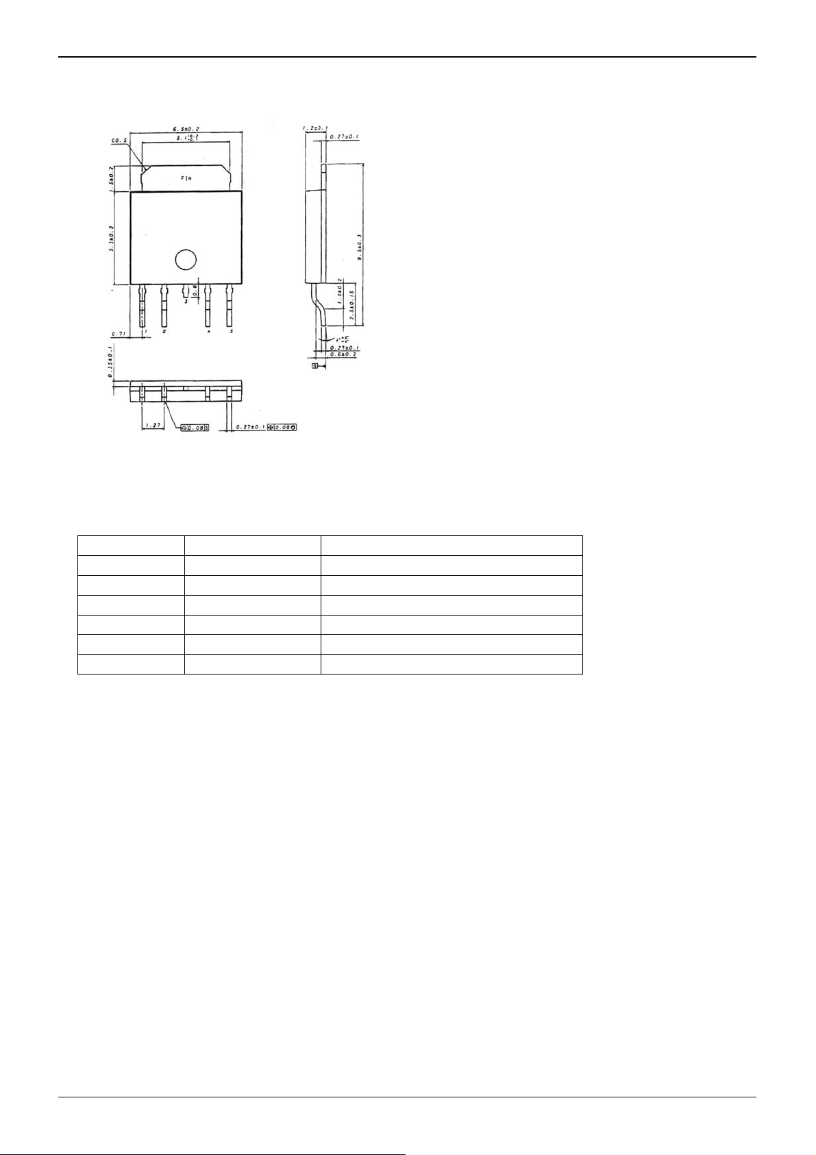
●I/O Equivalent Circuit
Pin 1 (Vcc, GND) Pin 2 (OUT) Pin 4 (INV) Pin 5 (STBY)
VCC
GND
VCC
OUT
VCC
INV
STBY
VCC
●Operation Notes
1. Absolute Maximum Rat ings
Exceeding the absolute maximum ratings (i.e. supply voltage, temperature) may cause damage to the device and make it
impossible to determine the failure mode (short/open). Therefore, when conditions exceeding the maximum ratings are
anticipated, consideration should be given to preventive countermeasures (e.g. fuses).
2. Application circuit
Although we can recommend the application circuits contained herein with a relatively high degree of confidence, we ask
that you verify all characteristics and specifications of the circuit as well as performance under actual conditions. Please
note that we cannot be held responsible for problems that may arise due to patent infringements or noncompliance with
any and all applicable laws and regulations.
3. Operating conditions
Proper operation is guaranteed under the recommended conditions/specifications.
4. GND voltage
Ensure that the GND fin is connected and is at the lowest potential under any operating conditions, includ ing transients.
5. Input supply voltage
Ensure that the Vcc pin is connected to the supply voltage.
6. Thermal design
Thermal designs should allow for sufficient margin for power dissipation under actual use.
7. Soldering
During mounting ensure that the OUT, Vcc, and GND pins are not shorted with one another. Carefully note IC orientation.
8. Operation in strong electromagnetic field
Operation in a strong electromagnetic field may cause malfunction.
9. Operation
The IC will turn ON when the voltage at the STBY pin is greater than 2.0V and will switch OFF if under 0.3V.
Therefore, do not input voltages between 0.3V and 2.0V. Malfunctions and/or physical damage may occur..
www.rohm.com
© 2009 ROHM Co., Ltd. All rights reserved.
9/11
2009.05 - Rev.A
Page 10

BD9870FPS
Technical Note
10.This IC is a monolithic IC which (as below) has P+ substrate and between
the various pin. A P-N junction is formed from this P layer of each pin. For example the relation between each potential is
as follows.(When GND > PinB and GND > PinA, the P-N junction operates as a parasitic diode.)
Parasitic diodes can occur inevitably in the structure of the IC. The operation of
parasitic diodes can result in mutual interference among circuits as well as operationfaults and physical damage.
Accordingly, you must not use methods by which parasitic diodesoperate, such as applying a voltage that is lower than the
GND(P substrate)voltage toan input pin.
●Power Dissipation
(PinA)
N
Parasitic diode
(PinA)
(W)
5
4
3
2
POWER DISSIPATION [Pd]
1
0
0 25 50 75 100 125
*When mounted on a 70mmx70mmx1.6mm board
Resistance
P
N
P substrate
GND
Parasitic diode
GND
③3.50W
②1.85W
①0.80W
(PinB)
~
~
+
P+
P
N
N N
Parasitic diode
~
~
Simplified structure of a Bipolar IC
Other adjacent components
①No heat sink
②2 layer PCB (Copper laminate area 15 mm×15mm)
③2 layer PCB (Copper laminate area 70 mm×70mm)
85
AMBIENT TEMPERA TURE [Ta]
C
(PinB)
B
N
N
P substrate
B
~
~
150
(℃)
Transistor (NPN)
~
~
P
GND
C
E
GND
E
+
P+
P
Parasitic diode
GND
www.rohm.com
© 2009 ROHM Co., Ltd. All rights reserved.
10/11
2009.05 - Rev.A
Page 11

BD9870FPS
●Ordering part number
B D 9 8 7 0 F P S - E 2
Part No.
TO252S-5
Part No.
6.5±0.2
C0.5
0.71
+0.2
5.1
−0.1
FIN
1.5±0.2
5.5±0.2
3
0.8
2
1
1.27
0.35±0.1
54
0.08 S
0.27±0.1
FPS = TO252S-5
Package
1.2±0.1
S
0.08
0.27±0.1
1.0±0.2
+6
4
–4
0.27±0.1
0.6±0.2
M
9.5±0.3
2.5±0.15
(Unit : mm)
<Tape and Reel information>
Embossed carrier tapeTape
Quantity
Direction
of feed
2000pcs
E2
The direction is the 1pin of product is at the lower left when you hold
( )
reel on the left hand and you pull out the tape on the right hand
Reel
1pin
Order quantity needs to be multiple of the minimum quantity.
∗
Packaging and forming specification
E2: Embossed tape and reel
(TO252S-5)
Technical Note
Direction of feed
www.rohm.com
© 2009 ROHM Co., Ltd. All rights reserved.
11/11
2009.05 - Rev.A
Page 12

Notes
No copying or reproduction of this document, in part or in whole, is permitted without the
consent of ROHM Co.,Ltd.
The content specied herein is subject to change for improvement without notice.
The content specied herein is for the purpose of introducing ROHM's products (hereinafter
"Products"). If you wish to use any such Product, please be sure to refer to the specications,
which can be obtained from ROHM upon request.
Examples of application circuits, circuit constants and any other information contained herein
illustrate the standard usage and operations of the Products. The peripheral conditions must
be taken into account when designing circuits for mass production.
Great care was taken in ensuring the accuracy of the information specied in this document.
However, should you incur any damage arising from any inaccuracy or misprint of such
information, ROHM shall bear no responsibility for such damage.
The technical information specied herein is intended only to show the typical functions of and
examples of application circuits for the Products. ROHM does not grant you, explicitly or
implicitly, any license to use or exercise intellectual property or other rights held by ROHM and
other par ties. ROHM shall bear no responsibility whatsoever for any dispute arising from the
use of such technical information.
Notice
The Products specied in this document are intended to be used with general-use electronic
equipment or devices (such as audio visual equipment, ofce-automation equipment, communication devices, electronic appliances and amusement devices).
The Products specied in this document are not designed to be radiation tolerant.
While ROHM always makes ef forts to enhance the quality and reliability of its Products, a
Product may fail or malfunction for a variety of reasons.
Please be sure to implement in your equipment using the Products safety measures to guard
against the possibility of physical injury, re or any other damage caused in the event of the
failure of any Product, such as derating, redundancy, re control and fail-safe designs. ROHM
shall bear no responsibility whatsoever for your use of any Product outside of the prescribed
scope or not in accordance with the instruction manual.
The Products are not designed or manufactured to be used with any equipment, device or
system which requires an extremely high level of reliability the failure or malfunction of which
may result in a direct threat to human life or create a risk of human injury (such as a medical
instrument, transportation equipment, aerospace machinery, nuclear-reactor controller,
fuel-controller or other safety device). ROHM shall bear no responsibility in any way for use of
any of the Products for the above special purposes. If a Product is intended to be used for any
such special purpose, please contact a ROHM sales representative before purchasing.
If you intend to export or ship overseas any Product or technology specied herein that may
be controlled under the Foreign Exchange and the Foreign Trade Law, you will be required to
obtain a license or permit under the Law.
www.rohm.com
© 2009 ROHM Co., Ltd. All rights reserved.
Thank you for your accessing to ROHM product informations.
More detail product informations and catalogs are available, please contact us.
ROHM Customer Support System
http://www.rohm.com/contact/
R0039
A
 Loading...