

Page 1

Large Current External FET Controller Type Switching Regulators
Single/Dual-output High-frequency
Step-down Switching Regulator(Controller type)
BD9853AFV
●Description
The BD9853AFV is a 2-ch synchronous DC/DC controller that can operate at a maximum switching frequency of 2MHz,
enabling the use of a smaller external coil than conventional lower-frequency switching regulators. This makes the
BD9853AFV a suitable choice for downsizing applications.
●Features
1) Synchronous Switching Regulator Controller 2channels
2) FET(Pch/Nch) Direct Drive
3) Adjustable Oscillator Frequency with External Resistor (Max. 2MHz)
4) Under Voltage Lockout Function (UVLO)
5) Thermal Shut Down Function (TSD)
6) Short Circuit Protection (SCP)
7) Independent ON/OFF Function in Each Channel with Soft Start Pin
8) SSOP-B16 Package
●Applications
TVSTB, PC, Portable CD・DVD,DVC etc.
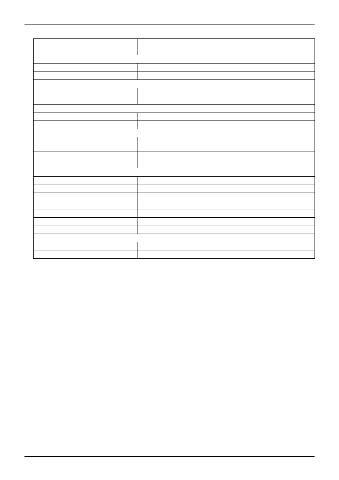
●Absolute Maximum Ratings (Ta = 25℃)
Parameter Symbol Limits Unit
Supply Voltage (VCC-GND) Vcc 18 V
VREGA-GND Voltage VREGA 7 V
VCC-VREGB Voltage VREGB 7 V
Power Dissipation Pd 562(*1) mW
Operating Temperature Range Topr -40 to +85 ℃
Junction Temperature Tjmax +150 ℃
Storage Temperature Range Tstg -55 to +150 ℃
* Reduced by 4.49mW for each increase in Ta of 1℃ over 25℃ (When mounted on a board 70×70×1.6tmm grass-epoxy PCB)
●Recommended Operating Conditions
Parameter Symbol
Supply Voltage Vcc 4.5 12 16 V
Oscillator Frequency fosc 100 1000 2000 KHz
SSOPB16
Limits
Min. Typ. Max.
No.09028EAT05
Unit
www.rohm.com
© 2009 ROHM Co., Ltd. All rights reserved.
1/16
2009.05 - Rev.A
Page 2
BD9853AFV
Technical Note
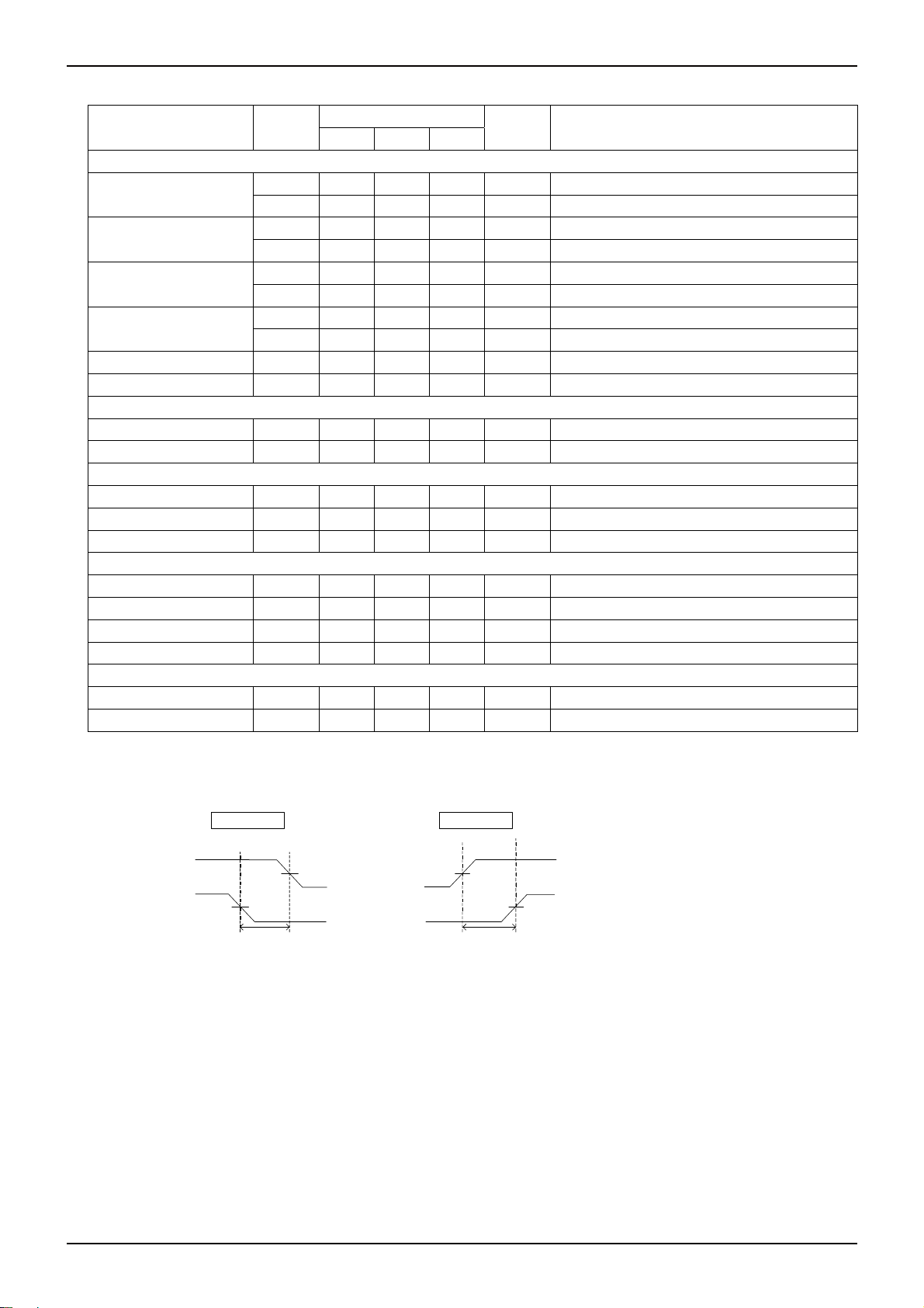
●Electrical Characteristics (Unless otherwise specified Ta=25℃,Vcc=12V,fosc=1000kHz,STB=3V)
Parameter Symbol
Min. Typ. Max.
Limits
Unit Conditions
【Whole Device】
Standby Current Iccst - 0 5 μASTB=0V
Circuit Current Icc - 3.2 5.2 mA INV1,INV2=2.5V
【Regulator for Driver REGA】
Output Voltage Vrega 4.5 5.0 5.5 V
Output Current Capability Irega - - -100 mA Vrega > 4.5V
【Regulator for Driver REGB】
Output Voltage Vregb VCC-5.5 VCC-5.0 VCC-4.5 V
Output Current Capability Iregb 100 - - mA Vregb < Vcc-4.5V
【Oscillator】
Oscillator Frequency fosc 900 1000 1100 kHz
RRT=8.2kΩ
OUTH=2200pF,OUTL=1000pF
Oscillator Frequency Coefficient1 Dfosc1 -2 0 2 % Vcc=4.5 to 5V
Oscillator Frequency Coefficient2 Dfosc2 -2 0 2 % Vcc=5 to 18V
【Error Amplifier】
Threshold Voltage Vthea 0.79 0.80 0.81 V
Input Bias Current Ibias -230 -115 - nA
Voltage Gain Av 60 80 100 dB DC GAIN
Max. Output Voltage Vfbh Vrega-0.85 - - V
Min. Output Voltage Vfbl - - 0.85 V
Output Sink Current Isink 2 11 - mA INV=2.5V, FB=2.5V
Output Source Current Isource - -15 -2 mA INV=0V, FB=2.5V
【PWM Comparator】
0% Threshold Voltage Vth0 1.4 1.5 1.6 V FB Voltage
100% Threshold Voltage Vth100 2.4 2.5 2.6 V FB Voltage
* This product is not designed for the protection against radioactive rays.
ROHM ROHM ROHM ROHM ROHM ROHM ROHM ROHM ROHM ROHM ROHM ROHM ROHM ROHM ROHM ROHM ROHM ROHM ROHM ROHM ROHM ROHM ROHM ROHM ROHM ROHM ROHM ROHM ROHM ROHM ROHM ROHM ROHM ROHM ROHM ROHM ROHM ROHM ROHM ROHM ROHM ROHM ROHM ROHM ROHM ROHM ROHM ROHM ROHM ROHM ROHM ROHM ROHM ROHM ROHM ROHM ROHM ROHM ROHM ROHM ROHM ROHM ROHM ROHM ROHM ROHM ROHM ROHM ROHM ROHM ROHM ROHM ROHM ROHM ROHM ROHM ROHM ROHM ROHM ROHM ROHM ROHM ROHM ROHM ROHM ROHM ROHM ROHM ROHM ROHM ROHM ROHM ROHM ROHM ROHM ROHM ROHM ROHM ROHM ROHM ROHM ROHM ROHM ROHM ROHM ROHM ROHM ROHM ROHM ROHM ROHM ROHM ROHM ROHM ROHM ROHM ROHM ROHM ROHM ROHM ROHM ROHM ROHM ROHM ROHM ROHM ROHM ROHM ROHM ROHM ROHM ROHM ROHM ROHM ROHM ROHM ROHM ROHM ROHM ROHM ROHM ROHM ROHM ROHM ROHM ROHM ROHM ROHM ROHM ROHM ROHM ROHM ROHM ROHM
www.rohm.com
© 2009 ROHM Co., Ltd. All rights reserved.
2/16
2009.05 - Rev.A
Page 3
BD9853AFV
Technical Note
●Electrical Characteristics (Unless otherwise specified, Ta=25℃,Vcc=12V,fosc=1000kHz,STB=3V)
Parameter Symbol
Min. Typ. Max.
Limits
Unit Conditions
【FET Driver】
On Resistance (OUT1H)
On Resistance (OUT1L)
On Resistance (OUT2H)
On Resistance (OUT2L)
RonP 1.6 3.2 4.8 Ω OUT=Hi
RonN 1.7 3.4 5.1 Ω OUT=Lo
RonP 1.6 3.2 4.8 Ω OUT=Hi
RonN 1.7 3.4 5.1 Ω OUT=Lo
RonP 1.6 3.2 4.5 Ω OUT=Hi
RonN 1.7 3.4 5.1 Ω OUT=Lo
RonP 1.6 3.2 4.8 Ω OUT=Hi
RonN 1.7 3.4 5.1 Ω OUT=Lo
Dead Time(Turn ON) tdtON 30 70 120 ns *OUTH,L H→L,OUTH=2200pF,OUTL=1000pF
Dead Time(Turn OFF) tdtOFF 25 60 115 ns *OUTH,L H→L,OUTH=2200pF,OUTL=1000pF
【Control Block】
Threshold Voltage Vstb 0.6 1.5 2.4 V
Sink Current Istb 6 15 30 μA
【Soft Start Block】
Soft Start Start-yo Voltage Vstasoft 0.2 0.3 0.4 V Output OFF when Vscp/SOFT<Vstass
Standby Voltage Vstsoft - - 40 mV SCP/SOFT Voltage
Source Current Isosoft -3.2 -2.3 -1.4 μA Vscp/SOFT=0.6V
【Short Circuit Protection (SCP)】
Timer Start Voltage Vtime 0.50 0.56 0.62 V INV Voltage
Threshold Voltage Vthscp 2.2 2.3 2.4 V SCP/SOFT Voltage
Standby Voltage Vstscp 1.21 1.35 1.49 V SCP/SOFT Voltage (When soft start ends)
Source Current Isoscp -3.2 -2.3 -1.4 μA SCP/SOFT=1.8V
【Under Voltage Lockout (UVLO)】
Threshold Voltage Vuvlo 4.0 4.15 4.30 V Vcc sweep down
Hysteresis Voltage DVuvlo 0.05 0.1 0.15 V
* This product is not designed for the protection against radioactive rays.
* Measurement of dead time
Turn ON Turn OFF
OUTH
OUTL
2.5V
tdtON
VCC-2.5V
VCC-2.5V
OUTH
2.5V
OUTL
tdtOFF
www.rohm.com
© 2009 ROHM Co., Ltd. All rights reserved.
3/16
2009.05 - Rev.A
Page 4

BD9853AFV
●Characteristic Data
100
90
80
70
60
50
ONDUTY[%]
40
30
20
10
0
1.31.41.51.61.71.81.92.02.12.22.32.42.52.6
OUTL
OUTH
FB VOLTAGE:VFB[V]
Fig.1 FB VOLTAGE VS ON DUTY
0
-1
-2
-3
-4
-5
-6
-7
-8
-9
-10
-11
-12
-13
-14
FB SOURCE CURRENT[mA]
-15
-16
-17
-18
-19
-20
0 0.2 0.4 0.6 0.8 1 1.2 1.4 1.6 1.8 2 2.2 2.4 2.6 2.8 3 3.2 3.4 3.6 3.8 4 4.2 4.4
OUTL SINK CURRENT:IOUT[mA]
Fig.4 FB SOURCE CURRENT
1000
950
900
850
800
750
700
650
600
550
500
450
400
350
300
250
200
150
100
50
0
0.00.20.40.60.81.01.21.41.61.82.02.22.42.62.83.03.23.43.63.84.0
Fig.7 OUTL SINK CURRENT
FB VOLTAGE[V]
VCC=12V,18V
VCC=4.5V
(OU TL-GN D) VO LTAGE [V]
180
160
140
120
100
80
60
40
20
0
-20
-40
-60
-80
GAIN[dB]、PHASE[deg]
-100
-120
-140
-160
-180
0.01 0.1 1 10 100 1000 10000 100000
Phase
Gain
FREQUENCY[KHz]
Fig.2 ERROR AMP OPEN LOOP
1000
950
900
850
800
750
700
650
600
550
500
450
400
350
300
250
200
150
OUTH SINK CURRENT:IOUT[mA]
100
50
0
0.0 0.2 0.4 0.6 0.8 1.0 1.2 1.4 1.6 1.8 2.0 2.2 2.4 2.6 2.8 3.0 3.2 3.4 3.6 3.8 4.0
VCC=12V,18V
4
VCC=4.5V
(REGB-OUTH) VOLTAGE[V]
Fig.5 OUTH SINK CURRENT
1000
950
900
850
800
750
700
650
600
550
500
450
400
350
300
250
200
150
100
OUTL SOURCE CURRENT:IOUT[mA]
50
0
0.0 0.2 0.4 0.6 0.8 1. 0 1.2 1.4 1.6 1. 8 2.0 2.2 2.4 2.6 2.8 3. 0 3.2 3.4 3. 6 3.8 4.0
VCC=12V,18V
VCC=4.5V
(REGA-OUTL) VOLTAGE[V]
Fig.8 OUTL SOURCE CURRENT
Technical Note
20
19
18
17
16
15
14
13
12
11
10
9
8
7
6
5
FB SINK CURRENT[mA]
4
3
2
1
0
0 0.2 0.4 0.6 0.8 1 1.2 1.4 1.6 1.8 2 2.2 2.4 2.6 2.8 3 3.2 3.4 3.6 3.8 4
Fig.3 FB SINK CURRENT
1000
950
900
850
800
750
700
650
600
550
500
450
400
350
300
250
200
150
100
50
OUTH SOURCE CURRENT:IOUT[mA]
0
0.00.20.40.60.81.01.21.41.61.82.02.22.42.62.83.03.23.43.63.84.0
Fig.6 OUTH SOURCE CURRENT
FB VOLTAGE[V]
VCC=12V,18V
VCC=4.5V
(VCC-OUTH) VOLTAGE:[V]
www.rohm.com
© 2009 ROHM Co., Ltd. All rights reserved.
4/16
2009.05 - Rev.A
Page 5
BD9853AFV
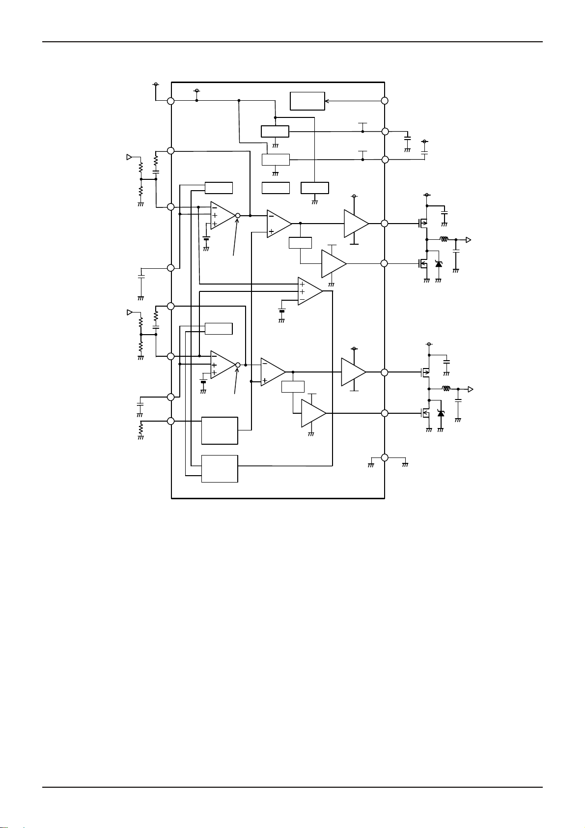
●Block Diagram
VOUT1
VCC
VCC
FB1
REGA
REGB
both channel
ON/OFF
5V
VCC-5V
Technical Note
STB
REGA
VCC
REGB
SCP/SOFT1
VOUT2
SCP/SOFT2
INV1
FB2
INV2
RT
SOFT1
0.8V
(Push-Pull)
SOFT2
0.8V
(Push-Pull)
OSC
Timer
Latch
0.56V
TSD
⊿ t
⊿ t
VREF
REGA
REGA
GND
REGB
GND
REGB
VCC
VCC
OUT1H
OUT1L
OUT2H
OUT2L
GND
VCC
Pch
VOUT1
Nch
VCC
Pch
VOUT2
Nch
Fig. 9
www.rohm.com
© 2009 ROHM Co., Ltd. All rights reserved.
5/16
2009.05 - Rev.A
Page 6

BD9853AFV
●Pin Configuration
Fig. 10
●Pin Description
Pin Number Pin Name Pin Descriptions
Technical Note
1 VCC Input Supply Voltage
2 OUT1H High Side (Main) FET Driver Output Pin (CH1)
3 OUT1L Low Side (Synchronous) FET Driver Output Pin (CH1)
4 REGA Internal Regulator Output Pin (5V Output, 1uF Ceramic Capacitor necessary)
5 RT Oscillator Frequency Adjustment Pin with external Resistor
6 FB1 Error Amplifier Output Pin (CH1)
7 INV1 Error Amplifer Negative Input Pin (CH1)
8 SCP/SOFT1 Short Circuit Protection・Soft Start Delay Time Setting Pin with External Capacitor (CH1)
9 SCP/SOFT2 Short Circuit Protection・Soft Start Delay Time Setting Pin with External Capacitor (CH2)
10 INV2 Error Amplifer Negative Input Pin (CH2)
11 FB2 Error Amplifier Output Pin (CH2)
12 GND Ground Pin
13 STB ON/OFF Control Pin
14 OUT2L Low Side (Synchronous) FET Driver Output Pin (CH2)
15 OUT2H High Side (Main) FET Driver Output Pin (CH2)
16 REGB Internal Regulator Output Pin (VCC-5V Output, 1uF Ceramic Capacitor necessary)
www.rohm.com
© 2009 ROHM Co., Ltd. All rights reserved.
6/16
2009.05 - Rev.A
Page 7

BD9853AFV
●Block functional descriptions
・Triangular wave oscillator
Connecting the resistor that sets the triangular wave oscillation frequency at the RT terminal generates the triangular wave,
which is input into the CH1 and CH2 PWM comparator.
・Error amp
The INV pin detects the output voltage, compares it to the programmed output voltage and amplifies the difference for
output by the FB pin. (The 0.8V reference is the comparison voltage. The tolerance is 1.25%.)
・PWM comparator
The PWM comparator converts the error amp (FB) voltage into a pulse width modulated waveform that goes to the FET
driver and turns FET output ON.
・FET driver
The push-pull FET driver directly drives the external MOSFET,providing high-side(OUT1H,OUT2H) switching at voltages
between Vcc⇔REGB, and low-side switching in the 0⇔REGA voltage range. (REGA = 5V; REGB= VCC -5V internal power)
・Standby function
The standby function enables output ON/OFF control by the STB pin. Output is ON when STB voltage is HIGH.
With the STB pin set HIGH, the output ON/OFF for each channel can be independently controlled by one of the
SCP/SOFT1, 2 pins.
・Soft Start/Short Circuit Protection (SCP)
Connecting the external capacitor on the SCP/SOFT1, 2 pins sets the SCP delay time and soft start time.
When STB is HIGH and the IC starts up, the capacitors on the SCP/SOFT1, 2 pins charge up at 2uA, stabilizing when the
system reaches 1.3V.
If load conditions change rapidly, causing the output voltage in either channel to fall to 70% or less of the set output voltage
(INV voltage 0.56 or lower), the SCP/SOFT1, 2 external capacitors will charge further until output for both channels
switches OFF at 2.3V.
・Under Voltage Lockout (UVLO)
Under Voltage lockout prevents IC malfunctions that could otherwise occur due to intermittent or fluctuating power supply
voltage, or insufficient voltage during start-up.When the VCC voltage falls to 4.1V or below, both channel outputs are
turned OFF, while the SCP/SOFT1, 2 pins are simultaneously set LOW.
The UVLO detection voltage includes 0.1V hysteresis width to prevent malfunctions from input voltage fluctuations.
・Thermal Shutdown (TSD)
The TSD circuit protects the IC against thermal runaway and heat damage.
・The TSD thermal sensor detects junction temperature. When the temperature reaches the TSD threshold (175℃), the
circuit switches the output of both channels OFF, and also switches REGA and REGB OFF. At the same time, it sets the
SCP/SOFT1, 2 pins LOW. The hysteresis width (15℃) provided between the TSD function start temperature (threshold)
and the stop temperature serves to prevent malfunctions from temperature fluctuations.
Technical Note
www.rohm.com
© 2009 ROHM Co., Ltd. All rights reserved.
7/16
2009.05 - Rev.A
Page 8
BD9853AFV
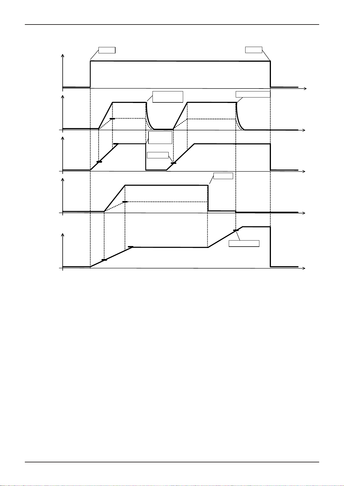
●Timing Chart
STB
STB ON
Technical Note
STB OFF
Vo1(solid line)
INV1
(dotted line)
SCP/SOFT1
Vo2
(solid line)
INV2
(dotted line)
SCP/SOFT2
0.3V
0.3V
0.8V
1.3V
0.8V
1.3V
Output OFF at
SCP/SOFT<0.3V
External GND short
(independent control)
Sort removed
SCP protection OFF
Output short
2.3V
End SCP delay
Fig. 11
www.rohm.com
© 2009 ROHM Co., Ltd. All rights reserved.
8/16
2009.05 - Rev.A
Page 9

BD9853AFV
●Application component selection and settings
Determining output voltage
Output voltage is determined by dividing the resistance of the
external resistors.
VOUT=0.8V×(1 + R2/R1)
determining the oscillation frequency
The oscillation pin is set by the resistor connected to the RT terminal (5 PIN).
10.000
INV
⑦ ⑩
Technical Note
OUT
V
R2
R1
1.000
RT
⑤
0.100
0.010
Oscillating Frequency(MHz)
0.001
1 10 100 1000
Timing Resistance(kΩ)
RRT
Selecting the external MOSFET
In the BD9853AFV design, the main side (OUT1H, OUT2H) is provided with an external PCH FET, while an NCH FET is
used on the synchronous rectification side (OUT1L, OUT 2L) .
FET selection should be made in conformance with the following relative configurations for maximum drain voltage (VDSS),
maximum gate source voltage (VGS), maximum output current, on-resistance RDS (ON) and gate capacitance (Ciss) loss:
・Maximum drain voltage (VDSS) is higher than the IC’s maximum input voltage (VIN).
・Maximum gate source voltage is higher than the IC gate driving voltage (REGA, VCC-REGB).
・Maximum output current is higher than the combined maximum load current and coil ripple current (⊿I
).
L
・The sum of on-resistance RDS (ON) and gate capacitance (Ciss) conduction loss, together with the switching loss,
must not exceed the power dissipation (pd) for the package.
FET conduction loss Phigh and Plow are defined as follows:
Phigh=Iout
Plow=Iout
2
×RDS(ON)×VOUT/VIN (PMOS conduction loss)
2
×RDS(ON)×(1-VOUT/VIN) (NMOS conduction loss)
Iout:output load current, RDS(ON) : FET ON resistance value, VIN : input voltage, Vout : output voltage
FET switching loss PSW is calculated as follows:
PSW=VIN/2×(tr + tf)×fosc×Iout
VIN : input voltage, tr : drain waveform rise time, tf : drain waveform fall time, fosc : oscillation frequency, lout : load current
In addition to the criteria for selecting individual MOSFET components, consideration must also be given to the
combination of the PMOS (main side) and NMOS (synchronous side) to be used. The configuration must not generate
any through current with PMOS and NMOS both ON at the same time. In order to meet this condition, the following
formula must be satisfied, where PCH, NCH MOSFET turn-on delay time is represented as tdON, MOSFET turn-off delay
time is tdOFF, and dead time is tdt.
tdt > tdON - tdOFF
The tdt turn-on is (OUTH,OUTL:H→L)70ns typ. Turn-off is OUTH,OUTL:L→H)70ns typ. Be sure to confirm that the
process delay time does not pose problem in terms of the overall MOSFET delay.
The following MOSFETs meet all of the selection criteria outlined above, and are recommended for use. Both are
manufactured by ROHM.
PCH: RSS040PO3 NCH: RSS065P03
www.rohm.com
© 2009 ROHM Co., Ltd. All rights reserved.
9/16
2009.05 - Rev.A
Page 10

yp)
BD9853AFV
Technical Note
Selecting the synchronous diode
An extremely low forward voltage Schottky barrier diode should be employed as the synchronous diode.
Selection of the specific diode to be used should be made in conformance with the following relative configurations for
maximum forward current, reverse voltage and diode power dissipation.
・The maximum current rating is higher than the combined maximum load current and coil ripple current (⊿I
・The reverse voltage rating is higher than the VIN value.
・Power dissipation for the selected diode must be within the rated level.
Synchronous diode power dissipation (Pdi) is expressed in the following formula:
Pdi=Iout(MAX)×tdt×fosc×Vf
Iout(MAX) : maximum load current, tdt: dead time 60ns typ,fosc : oscillation frequency, Vf:forward voltage
Selecting the output/input coil
The output coil and the output capacitor together form a second-order smoothing filter for the switch waveform and provide
the DC output voltage.
If a coil’s inductor value is low, its physical size is minimized, but the penalty is higher ripple current, with lowered efficiency
and an increase in output noise. Conversely, a higher inductor value increases the size of the coil, but lowers the ripple
current and, consequently. the output ripple current.
Generally speaking, ripple current should be between 20% and 50% of output load current. The following equation is used
to calculate the inductor value that corresponds to the ripple current value being employed.
(V
L=
L:inductor value, V
fosc:oscillation frequency, I
IN-VOUT)
⊿I
L
:maximum input voltage, V
IN
V
OUT
××
V
IN
:output load current
OUT
f
OSC
OUT
1
=(0.2 to 0.5)×I
⊿I
L
,
OUT
:output voltage, ⊿IL:coil ripple current value
Note that the current rating for the coil should be higher than I
Selecting the input capacitor
The input capacitor is the source of current that flows to the coil via the FET whenever the high side MOSFET is ON. In
selecting an input capacitor, sufficient margin must be provided to accommodate capacitor pressure and the permissible
ripple current.
The expression below defines the effective value of the ripple current to the input capacitor. It should be used in
determining the suitability of the capacitor in providing sufficient margin for the permissible ripple current.
I
I
I
RMS=IOUT
: effective value of the ripple current to the input capacitor
RMS
: output load current
OUT
×√
(1-V
OUT/VIN
)×V
OUT/VIN
Selecting the output capacitor
The output capacitor should confine ESR and permissible ripple current within a stable region.
Although incorporating a low-ESR capacitor will limit ripple voltage and load fluctuation, it can also hurt the stability of the
feedback network. Therefore, in order to maintain a stable feedback loop when ceramic or other low-ESR capacitors are
employed, special attention must be paid to providing an appropriate phase compensation scheme.
A suitable output capacitor will satisfy the following formula for ESR.
ESR≦⊿V
⊿V
/⊿IL
L
: permissible ripple voltage, ⊿IL : coil ripple current
L
In addition, use the following formula to determine the effective value of the output capacitance permissible ripple current,
and select a capacitor that allows sufficient margin to accommodate this value.
=⊿IL/2√3
I
RMS
: effective value of ripple current to the output condenser, ⊿IL : coil ripple current
I
RMS
Setting the soft start time
To prevent output voltage startup overshoot on either channel, the capacitors connected to the SCP/SOFT 1, 2 pins – in a
discharged state at power-on – are gradually charged during a delay interval, thus providing a soft start. The soft start
period is the time from when the standby pins go from LOW to HIGH, starting the charge, to the time that the output
voltage reaches the programmed setting. The soft start time is calculated in the following equation:
tsoft=
0.8[V] (t
×Cscp/soft[F]
Isosoft (typ: 2.3μA)[A]
tsoft : soft start time, Cscp/soft : SCP/SOFT pin connection capacitance, Isosoft : charge current
(MAX)+⊿IL.
OUT
).
L
www.rohm.com
© 2009 ROHM Co., Ltd. All rights reserved.
10/16
2009.05 - Rev.A
Page 11

BD9853AFV
Technical Note
Setting the Short Circuit Protection (SCP) delay time
When the soft start is complete for each channel, the output voltage stabilizes at the set value 1.35V(typ) for the
SCP/SOFT1, 2 pins.
When any type of short circuit occurs, the voltage at the point of the fault is reduced. In this case, when voltage at the INV
pin falls to 0.56V(typ) or below, the SCP comparator sensor detects the short and further charges the SCP/SOFT pins for
the shorted channel from the 1.35V(typ) level. When the SCP/SOFT pins are charged to 2.3V(typ), the Pch/Nch MOSFET
is switched OFF.
The elapsed time from the occurrence of the output short to the point the external FET switches OFF is calculated with the
following formula:
tscp
0.95[V](typ)×Cscp/soft[F]
=
Isosofc (typ: 2.3μA)[A]
tscp : SCP delay time, Cscp/soft : SCP/SOFT pin connection capacitance,Isoscp : charge current
* If the current more than the capacity of power supply when the short between VOUT and GND occurs, input voltage starts to fall and under voltage lockout
(UVLO) is activated at Vin < 4.15 V (typ.). The UVLO has FET driver output (OUT1H, OUT2H, OUT1L, OUT2L) off and external FETs become off. When
external FETs are not operating, input voltage returns because of the short between VOUT and GND and the UVLO is canceled. But input voltage starts to
fall again because the UVLO is not activated.
There is possibility that a series of behavior “output short → input voltage fall → UVLO activated → external FETs off → input voltage returns → UVLO
canceled → output short”. So please make provision like inserting FUSE in input line.
Pin conditions with the only single channel use
Pin conditions are shown in the following, when the only single channel out of 2 channels is used.
Use only CH1 Use only CH2
・SCP/SOFT2, INV2 ⇒ GND short ・SCP/SOFT1, INV1 ⇒ GND short
・FB2, OUT2H, OUT2L ⇒ OPEN ・FB1, OUT1H, OUT1L ⇒ OPEN
●Application example
VCC
VCC
VCC
VCC
OUT1H
OUT1L
REGA
RT
FB1
INV1
SCP/SOFT1
1μF
REGB
OUT2H
OUT2L
STB
GND
FB2
INV2
SCP/SOFT2
4.7μF
16
15
14
13
12
11
220pF
10
9
3.3kΩ
RSS040P03
(ROHM)
VCC
RSS065
(ROHM)
NO3
4.7μH
C6-K3L
(MITSUMI)
RB081
L-20
(ROHM)
10μF
(ceramic)
10kΩ
120pF
VOUT1
(3.3V)
22kΩ
100kΩ
39kΩ
10μF
(ceramic)
4.7μF
4.7μH
C6-K3L
(MITSUMI)
RB081
L-20
(ROHM)
0.1μF
1μF
8.2kΩ
680pF
1
2
3
4
5
6
7
8
RSS040P03
(ROHM)
10kΩ
RSS065
NO3
(ROHM)
0.015μF 0.015μF
100kΩ
47kΩ
VOUT2
(2.5V)
15kΩ
68pF
www.rohm.com
© 2009 ROHM Co., Ltd. All rights reserved.
11/ 16
2009.05 - Rev.A
Page 12
BD9853AFV
Technical Note
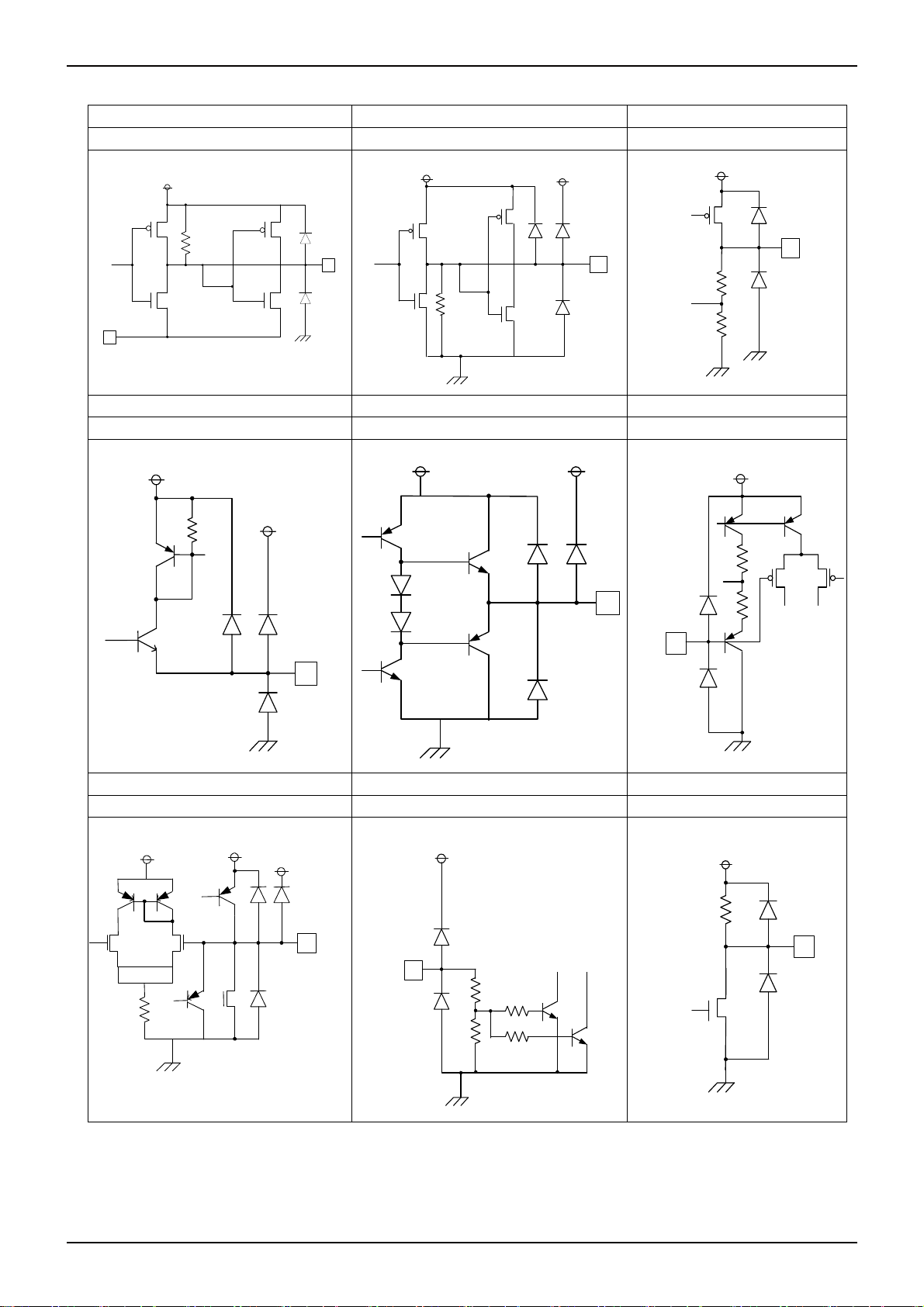
●I/O Equivalent Circuit
OUT1H(2),OUT2H(15) OUT1L(3),OUT2L(14) REGA(4)
Max ratings:7V(from VCC or REGB) Max ratings:7V Max ratings:7V
VCC
VCCREGA
VCC
REGA
REGB
OUT1H
OUT2H
OUT1L
OUT2L
RT(5) FB1(6),FB2(11) INV1(7),INV2(10)
Max ratings:7V Max ratings:7V Max ratings:10V
REGA
REGA
VCC
VCC
VCC
INV1
INV2
RT
SCP/SOFT1(8),SCP/SOFT2(9) STB(13) REGB(16)
Max ratings:7V Max ratings:18V Max ratings:7V(fromVCC)
VREF
REGA
VCC
SCP/SOFT1
SCP/SOFT2
STB
VCC
VCC
REGB
www.rohm.com
© 2009 ROHM Co., Ltd. All rights reserved.
12/16
2009.05 - Rev.A
Page 13
BD9853AFV
Technical Note
●Recommended Board Patterns
P
MOS
V
OUT
C
IN
N
MOS
SBD
C
OUT
GND(IC)
INV
GND(others)
There are two current loops at the behavior of switching regulator. When laying a pattern on the board, put these elements
near to minimize these current loops and make the lines as short and wide as possible. And connect all GND lines at one
point to reduce effects caused by above current noise to other lines.
a pattern example of switching part
OUT
C
L
SBD
MOS
MOS
N
P
IN
C
Place following parts with attention about patterns
VCC REGB
CREGB
GND
CVCC
1
REGB
16VCC
GND
CREGA
RRT
2
3
4
REGA
5
RT
6
7
8
15
14
13
12
11
10
9
・Place CVCC, CREGA, RRT, CREGB as near to the pin as possible.
・Pattern area has to be small enough to reduce parasitic capacitance with RT terminal.
www.rohm.com
© 2009 ROHM Co., Ltd. All rights reserved.
13/16
2009.05 - Rev.A
Page 14

BD9853AFV
Technical Note
●Notes for use
1) Absolute maximum ratings
Use of the IC in excess of absolute maximum ratings such as the applied voltage or operating temperature range may
result in IC deterioration or damage. Assumptions should not be made regarding the state of the IC (short mode or open
mode) when such damage is suffered. A physical safety measure such as a fuse should be implemented when use of the
IC in a special mode where the absolute maximum ratings may be exceeded is anticipated.
2) GND potential
Ensure a minimum GND pin potential in all operating conditions. In addition, ensure that no pins other than the GND pin
carry a voltage lower than or equal to the GND pin, including during actual transient phenomena.
3) Thermal design
Use a thermal design that allows for a sufficient margin in light of the power dissipation (Pd) in actual operating conditions.
4) Inter-pin shorts and mounting errors
Use caution when orienting and positioning the IC for mounting on printed circuit boards. Improper mounting may result in
damage to the IC. Shorts between output pins or between output pins and the power supply and GND pin caused by the
presence of a foreign object may result in damage to the IC.
5) Operation in a strong electromagnetic field
Use caution when using the IC in the presence of a strong electromagnetic field as doing so may cause the IC to
malfunction.
6) Thermal shutdown circuit (TSD circuit)
This IC incorporates a built-in thermal shutdown circuit (TSD circuit). The TSD circuit is designed only to shut the IC off to
prevent runaway thermal operation. Do not continue to use the IC after operating this circuit or use the IC in an
environment where the operation of the thermal shutdown circuit is assumed.
7) Testing on application boards
When testing the IC on an application board, connecting a capacitor to a pin with low impedance subjects the IC to stress.
Always discharge capacitors after each process or step. Ground the IC during assembly steps as an antistatic measure,
and use similar caution when transporting or storing the IC. Always turn the IC's power supply off before connecting it to or
removing it from a jig or fixture during the inspection process.
8) Common impedance
Power supply and ground wiring should reflect consideration of the need to lower common impedance and minimize ripple
as much as possible
(by making wiring as short and thick as possible or rejecting ripple by incorporating inductance and capacitance).
9) Applications with modes that reverse VCC and pin potentials may cause damage to internal IC circuits.
For example, such damage might occur when VCC is shorted with the GND pin while an external capacitor is charged.
It is recommended to insert a diode for preventing back current flow in series with VCC or bypass diodes between VCC
and each pin.
Bypass diode
Back current prevention diode
VCC
Output Pin
10) Pin short and mistake fitting
Do not short-circuit between OUT pin and VCC pin, OUT pin and GND pin, or VCC pin and GND pin.
When soldering the IC on circuit board,
please be unusually cautious about the orientation and the position of the IC.
11) Timing resistor and capacitor
Timing resistor connected between RT and GND, has to be placed near RT terminal. And pattern has to be short enough.
www.rohm.com
© 2009 ROHM Co., Ltd. All rights reserved.
14/16
2009.05 - Rev.A
Page 15

BD9853AFV
Technical Note
12) IC pin input
This monolithic IC contains P+ isolation and PCB layers between adjacent elements in order to keep them isolated.
P/N junctions are formed at the intersection of these P layers with the N layers of other elements to create a variety of
parasitic elements. For example, when a resistor and transistor are connected to pins as shown in following chart,
the P/N junction functions as a parasitic diode
when GND > (Pin A) for the resistor or GND > (Pin B) for the transistor (NPN).
Similarly, when GND > (Pin B) for the transistor (NPN),
the parasitic diode described above combines with the N layer of other adjacent elements to operate as a parasitic
NPN transistor.
The formation of parasitic elements as a result of the relationships of the potentials of different pins is an inevitable result
of the IC's architecture. The operation of parasitic elements can cause interference with circuit operation as well as IC
malfunction and damage. For these reasons, it is necessary to use caution so that the IC is not used in a way that will
trigger the operation of parasitic elements, such as by the application of voltages lower than the GND (PCB) voltage to
input and output pins.
Resistance
+
P
N
Parasitic diode
P
N
P substrate
GND
Transistor (NPN)
(PinB)(PinA)
+
P
N
Parasitic elementals
N
B
N
P
N
P substrate
GND
E
GND
+
P
N
Other adiacent components
C
+
P
(PinA)
(PinB)
Parasitic diode
GND
B
GND
C
E
Parasitic diode
●Power Dissipation Reduction
1000
800
600
400
200
POWER DISSIPATION : Pd(mW)
0
※IC mounted on a ROHM standard board
(70mm X 70mm X 1.6mm, glass epoxy)
0 25 50 75 100 125 150 175
AMBIENT TEMPERATURE:Ta (℃)
www.rohm.com
© 2009 ROHM Co., Ltd. All rights reserved.
15/16
2009.05 - Rev.A
Page 16

BD9853AFV
●Ordering part number
B D 9 8 5 3 A F V - E 2
Part No.
SSOP-B16
Part No.
5.0±0.2
16
4.4±0.2
6.4±0.3
1
1.15±0.1
0.10
0.65
9
0.3Min.
8
0.15±0.1
0.1
0.22±0.1
(Unit : mm)
Package
FV:
SSOP-B16
<Tape and Reel information>
Embossed carrier tapeTape
Quantity
Direction
of feed
2500pcs
E2
The direction is the 1pin of product is at the upper left when you hold
()
reel on the left hand and you pull out the tape on the right hand
Reel
Packaging and forming specification
E2: Embossed tape and reel
1pin
Order quantity needs to be multiple of the minimum quantity.
∗
Direction of feed
Technical Note
www.rohm.com
© 2009 ROHM Co., Ltd. All rights reserved.
16/16
2009.05 - Rev.A
Page 17

Notes
No copying or reproduction of this document, in part or in whole, is permitted without the
consent of ROHM Co.,Ltd.
The content specied herein is subject to change for improvement without notice.
The content specied herein is for the purpose of introducing ROHM's products (hereinafter
"Products"). If you wish to use any such Product, please be sure to refer to the specications,
which can be obtained from ROHM upon request.
Examples of application circuits, circuit constants and any other information contained herein
illustrate the standard usage and operations of the Products. The peripheral conditions must
be taken into account when designing circuits for mass production.
Great care was taken in ensuring the accuracy of the information specied in this document.
However, should you incur any damage arising from any inaccuracy or misprint of such
information, ROHM shall bear no responsibility for such damage.
The technical information specied herein is intended only to show the typical functions of and
examples of application circuits for the Products. ROHM does not grant you, explicitly or
implicitly, any license to use or exercise intellectual property or other rights held by ROHM and
other par ties. ROHM shall bear no responsibility whatsoever for any dispute arising from the
use of such technical information.
Notice
The Products specied in this document are intended to be used with general-use electronic
equipment or devices (such as audio visual equipment, ofce-automation equipment, communication devices, electronic appliances and amusement devices).
The Products specied in this document are not designed to be radiation tolerant.
While ROHM always makes efforts to enhance the quality and reliability of its Products, a
Product may fail or malfunction for a variety of reasons.
Please be sure to implement in your equipment using the Products safety measures to guard
against the possibility of physical injury, re or any other damage caused in the event of the
failure of any Product, such as derating, redundancy, re control and fail-safe designs. ROHM
shall bear no responsibility whatsoever for your use of any Product outside of the prescribed
scope or not in accordance with the instruction manual.
The Products are not designed or manufactured to be used with any equipment, device or
system which requires an extremely high level of reliability the failure or malfunction of which
may result in a direct threat to human life or create a risk of human injury (such as a medical
instrument, transportation equipment, aerospace machinery, nuclear-reactor controller,
fuel-controller or other safety device). ROHM shall bear no responsibility in any way for use of
any of the Products for the above special purposes. If a Product is intended to be used for any
such special purpose, please contact a ROHM sales representative before purchasing.
If you intend to export or ship overseas any Product or technology specied herein that may
be controlled under the Foreign Exchange and the Foreign Trade Law, you will be required to
obtain a license or permit under the Law.
www.rohm.com
© 2009 ROHM Co., Ltd. All rights reserved.
Thank you for your accessing to ROHM product informations.
More detail product informations and catalogs are available, please contact us.
ROHM Customer Support System
http://www.rohm.com/contact/
R0039
A
 Loading...