

Page 1

TECHNICAL NOTE
Large Current External FET Controller Type Switching Regulators
Single-output High-frequency Step-down
Switching Regulator
BD9850FVM
(Controller type)
Dual-output Step-up, Negative, Step-down
High temperature
operating
Now available
ESD
Resistance
Now available
Switching Regulator
(Controller type)
BD9851EFV
Description
The BD9850FVM is a 1-channel DC/DC step-down switching regulator controller, while the BD9851EFV is a 2-channel DC/DC
step-down switching regulator controller. The BD9850FVM is adaptable for a maximum switching frequency of 2 MHz and the
BD9851EFV for that of 3 MHz. Both provide space saving in all applications.
Features
1) Adaptable for 2-MHz switching frequency (externally variable) (BD9850FVM)
Adaptable for 3-MHz switching frequency (externally variable) (BD9851EFV)
2) FET direct drive
3) High-accuracy reference voltage (Accuracy: ±1%)
4) Built-in Under Voltage Lock Out circuit (UVLO)
5) Built-in Thermal Shutdown circuit (TSD)
6) The BD9851EFV provides two channels:
Channel 1 available for selection of step-down/step-up switching
Channel 2 available for selection of step-down/inverting switching.
7) Compact MSOP8 package (BD9850FVM) / HTSSOP-B20 package (BD9851EFV)
Applications
TFT panel, TA/ Router, digital consumer electronics, PC, and portable CD/DVD/DVC
Product lineup
BD9850FVM
Input range
Oscillation frequency range
External synchronization
Standby function
Operating temperature
Package
4V to 9V
100kHz to 2MHz
Not provided
Not provided
–40˚C to 85˚C
MSOP8
ROHM CO., LTD .
BD9851EFV
4V to 18V
10kHz to 3MHz
Not provided
Provided
–40˚C to 85˚C
HTSSOP-B20
Sep. 2008
Page 2

Absolute maximum ratings (Ta=25˚C)
BD9850FVM
Item
Power supply voltage
Storage temperature
Operating temperature
Power dissipation
Maximum junction temperature
Reduce by 4.7 mW/ºC over 25ºC (When mounted on PCB of 70mm×70mm×1.6mm)
*
Symbol Rating Unit
Vcc
Tst g
Topr
Pd
Tjmax
10
–55 to +150
–40 to +85
*
587
+150
BD9851EFV
Item
Power supply voltage
(Between
Vcc and GND)
Between VREF and GND
Between OUT1 and PVcc1
Between OUT2 and PVcc2
Between OUT1, OUT2 and PGND
Power dissipation
Operating temperature
Maximum junction temperature
Storage temperature
Symbol Rating Unit
Vcc
REF
V
Vouth
Voutl
Pd
Topr
Tjmax
Tst g
20
7
20
20
(*)
1000
–40 to +85
+150
–55 to +150
(*)Reduce by 8.0 mW/ºC over 25ºC (When mounted on PCB of 70mm×70mm×1.6mm)
V
ºC
ºC
mW
ºC
V
V
V
V
mW
ºC
ºC
ºC
Recommended operating range
BD9850FVM
Item
Power supply voltage
Oscillation frequency
Operating temperature
BD9851EFV
Item
Power supply voltage
Oscillation frequency
Timing resistor
Timing capacitor
Symbol
Vcc
fosc
Topr
Symbol
Vcc
fosc
RT
R
CCT
4
100
–40
4
10
3.3
33
Limits
Typ. max.min.
7
–
–
Limits
Typ. max.min.
12
300
–
–
9
2000
+85
18
3000
47
10000
Unit
V
kHz
ºC
Unit
V
kHz
kΩ
pF
2/16
Page 3

BD9850FVM
Electrical characteristics (Unless otherwise specied, Ta=25˚C, Vcc=7V, fosc=600kHz)
Item Symbol
Limits
Typ. max.min.
[Oscillator block]
Oscillation frequency
Frequency regulation
Oscillator amplitude voltage
fosc
FDV
Vpptr
510
–5
–
600
0
0.5
690
5
–
[Soft start /SW block]
CTL /SS pin sink current
CTL /SS pin clamp voltage
CTL threshold voltage
ISS
VSS
VCTLTH
–1.90
2.2
1.2
–1.00
2.4
1.3
1.00
2.6
1.4
[PWM comparator block]
Unit
kHz
%
V
μA
V
V
Conditions
RT = 24kΩ
R
Vcc = 4V to 9V
*
VCTL/SS = 1.5V
0% threshold voltage
100% threshold voltage
[Error Amp block]
Threshold voltage
Frequency bandwidth
Voltage gain
Input bias current
Maximum output voltage
Minimum output voltage
Output source current
Output sink current
REF block]
[V
REF output voltage
V
REF load regulation
F
REF current capacitance
V
[Total device]
Standby current
Average supply current
[Output block]
D0
D100
V
IN
BW
Av
IIB
VCH
VCL
IOl
IOO
REF
V
ΔVREFl0
IVREF
ICCS
ICCA
1.5
2.0
0.98
1.5
–
–150
2.3
–
–3.1
12
2.475
–
–45
420
3.4
1.6
2.1
1.00
3.0
70
–70
2.4
0.03
–1.6
50
2.500
–
–16
610
5.0
1.7
2.2
1.02
–
–
–
2.6
0.20
–1.0
125
2.525
10
–1
960
7.8
V
V
V
MHz
dB
hA
V
V
mA
mA
V
mV
mA
μA
mA
fosc = 600kHz
fosc = 600kHz
AV = 0dB
*
*
V
FB = 1.0V
FB = 1.0V
V
I
VREF = 0mA
VREF = 0mA to –1mA
I
At no load
ON resistance
Output transient time
[Under voltage lockout block]
Threshold voltage
Hysteresis width
Design guarantee
*
Not designed to be radiation-resistant.
*
R
ON
Tr/ Tf
VUT
VUThy
0.9
–
3.7
0.05
2.5
20
3.8
0.10
3/16
8.0
–
3.9
0.15
Ω
nsec
V
V
Cout = 1000pF
Vcc sweep down
*
Page 4

BD9851EFV
Electrical characteristics (Unless otherwise specied, Ta=25˚C, Vcc=12V, fosc=300kHz, STB=3V)
Item Symbol
Limits
Typ. max.min.
Unit
[Total device]
Standby mode circuit current
Operation mode circuit current
Iccst
Icc
1.5
–
–
2.5
5
4.1
μA
mA
[Reference voltage block]
REF
Output voltage
Input stability
V
DVli
2.475
–
2.500
–
2.525
10
V
mV
Conditions
STB=0V
FB1, FB2=0V
Io=–0.1mA
Vcc= 4Vto18V, Io=–0.1mA
Load stability
Short circuit mode output current
[Oscillator block]
Oscillation frequency
Oscillation frequency regulation
[Error Amp block]
Threshold voltage
Input oset voltage
Common-mode input voltage range
Input bias current
Voltage gain
Frequency bandwidth
Maximum output voltage
Minimum output voltage
Output sink current
Output source current
[PWM comparator block]
0% threshold voltage
100% threshold voltage
DTC bias current
[FET driver block]
ON resistance
DVlo
Ios
fosc
Dfosc
Vthea
Vofst
Vcm
Ibias
Av
Bw
Vfbh
Vfbl
Isink
Isource
Vth0
Vth100
Idtc
R
ONN
R
ONP
–45
270
–2
0.98
–10
0.3
–150
60
REF –0.1
V
1.6
–260
1.21
1.74
–1
1.5
–
3
–
1
–
–12
300
0
1.00
0
–
–70
75
6
–
–
6
–160
1.31
1.84
–
3
2
10
–3
330
2
1.02
10
2.0
–
90
13
REF
V
0.1
16
–90
1.41
1.94
1
3
2
mV
mA
kHz
%
mV
nA
dB
MHz
mA
μA
μA
Ω
Ω
Io=–0.1mA to –1mA
R
RT=24kΩ, CCT=220pF
Vcc= 4Vto18V
Ch1
V
Ch2
Ch2
V
DC
MHz
V
V
FB pin
FB pin
FB voltage
V
FB voltage
V
When OUT=Lo
When OUT=Hi
*Design guarantee
*Design guarantee
SEL1 input voltage range
[Control block]
Threshold voltage
Sink current
[Short circuit protection circuit (SCP) block]
Timer start voltage
Threshold voltage
Standby mode voltage
Source current
Vthscp
Vstscp
Vsoscp
[Under voltage lockout block (UVLO)]
Threshold voltage
Hysteresis width
Design guarantee
*
DVuvlo
Vselh
Vsell
Vstb
Istb
Vtime
Vuvlo
Vcc– 0.2
0
0.6
6
2.2
1.4
–
–3.2
3.58
0.05
–
–
1.5
15
2.3
1.5
10
–2.0
3.7
0.11
4/16
–
–
1.5
15
2.3
1.5
10
–2.0
3.7
0.11
V
V
V
μA
V
V
mV
μA
V
V
In step-down switching
In step-down switching
STB=3V
FB voltage
SCP voltage
SCP voltage
SCP=0.75V
Vcc sweep down
Page 5

Characteristic data
(BD9850FVM)
1.02
1.015
1.01
1.005
1
0.995
0.99
0.985
0.98
–40 –20 0 20 40 60 80
ERROR-AMP. THRESHOLD VOLTAGE : VINV(V )
AMBIENT TEMPERATURE : Ta(˚C) FB VOLTAGE : VFB(V )
100
90
87
70
60
50
40
30
ON DUTY : DON(%)
20
10
0
1.5 1.6 1.7 1.8 1.9 2 2.1 2.2
Fig.1 Error Amp threshold voltage vs. Ambient temperature Fig.2 FB voltage vs. ON Duty
1000
900
800
700
600
500
400
300
200
100
OUT SOURCE CURRENT : IOUT [mA]
0
0 0.25 0.5 0.75 1 1.25 1.5 1.75 2
(VCC-OUT)VOLTAGE : VO(V)
Vcc=10V
Vcc=7V
Vcc=4V
1000
900
800
700
600
500
400
300
200
100
OUT SINK CURRENT : IOUT [mA]
0 0.25 0.5 0.75 1 1.25 1.5 1.75 2
Vcc=10V
OUT VOLTAGE : VO(V )
Vcc=7V
Vcc=4V
Fig.3 (Vcc-OUT) Voltage vs. Output source current
2.53
2.52
2.51
[V]
REF
2.5
2.49
VOLTAGE:V
REF
V
2.48
2.47
–40 –20 0 20 40 60 80 –40 –20 0 20 40 60 80
AMBIENT TEMPERATURE : Ta [˚C] AMBIENT TEMPERATURE : Ta [˚C]
Fig.5 V
REF vs. Ambient temperature Fig.6 Oscillation frequency vs. Ambient temperature
Fig.4 Output voltage vs. Output sink current
650
640
630
620
610
RT=24kΩ
600
590
580
570
560
OSCILLATING FREQUENCY : FOSC [kHz]
550
5/16
Page 6

(BD9851EFV)
1.02
1.015
1.01
1.005
1
0.995
0.99
0.985
0.98
–40 –20 0 20 40 60 80
ERROR-AMP. THRESHOLD VOLTAGE : VEATH (V)
AMBIENT TEMPERATURE : Ta(˚C)
Fig.7 Error Amp threshold voltage vs. Ambient temperature
1000
900
800
700
600
500
400
300
200
100
OUT SOURCE CURRENT : IOUT (mA)REFERENCE VOLTAGE : VREF (V )
0
0 0.5 1 1.5 2 2.5 3 3.5 4
Vcc=20V
Vcc=12V
Vcc=4V
(Vcc-OUT) VOLTAGE : VO(V)
Fig.9 (Vcc-OUT) Voltage vs. Output source current
100
90
80
70
60
50
40
30
ON DUTY : DON (%)
fosc=1MHz
20
10
0
1.2 1.3 1.4 1.5 1.6 1.7 1.8 19
fosc=300kHz
DTC VOLTAGE : VDTC (V)
Fig.8 FB voltage vs. ON Duty
1000
900
800
700
600
OUT (mA)
500
400
300
200
100
0
0 0.5 0 1.5 2 2.5 3 3.5 4
Vcc=20V
Vcc=12V
Vcc=4V
OUT VOLTAGE : VO (V )
Fig.10 Output voltage vs. Output sink current
2.55
2.54
2.53
2.52
2.51
2.5
2.49
2.48
2.47
2.46
2.45
–40 –20 0 20 40 60 80
320
315
310
305
300
295
290
285
OSCILLATING FREQUENCY : FOSC (kHz) OUT SINK CURRENT : I
280
–40 –20 0 20 40 60 80
AMBIENT TEMPERATURE : Ta(˚C) AMBIENT TEMPERATURE : Ta(˚C)
Fig.11 V
REF vs. Ambient temperature
Fig.12 Oscillation frequency vs. Ambient temperature
RRT=24kΩ
CCT=220pF
6/16
Page 7
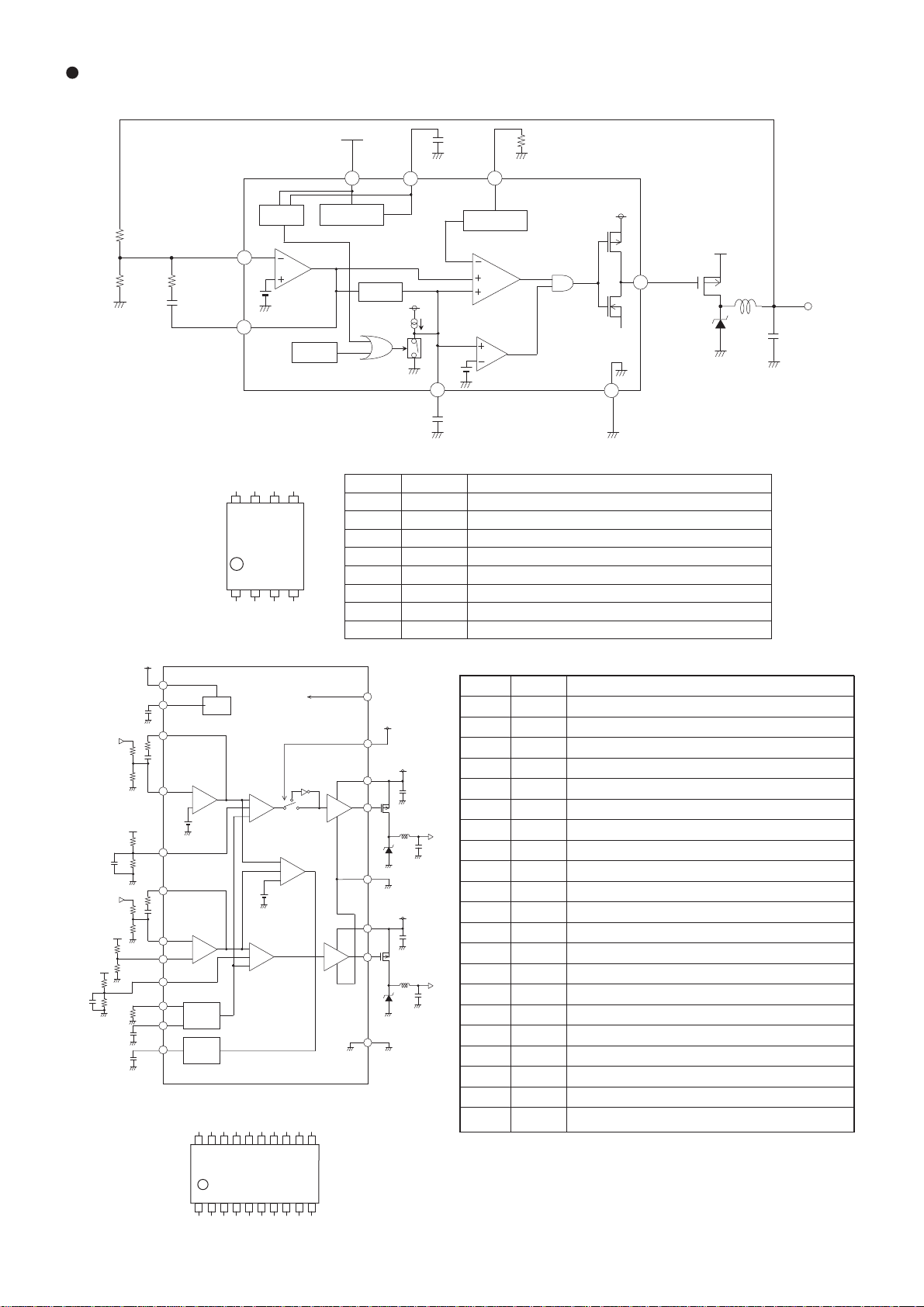
Block diagram / Pin assignment
(BD9850FVM)
Vcc
(BD9851EFV)
Vcc
V
Vo1
VREF
DTC1
Vo2
VREF
NON2
VREF
DTC2
U.V.L.O
5
INV
Error Amp
1.0V
6
FB
T.S.D
OUT CTL/ SS
–
–
+
–
–
+
GND FB
Both channels
ON/OFF
+
+
–
2.3V
REF INV
V
Vcc R T
Vcc
18
REF
17
FB1
15
16
INV1
13
FB2
6
5
INV1
4
7
RT
2
CT
3
SCP
14
+
1V
–
+
OSC
Tmer
Latch
REF
V
(2.5V)
–
Fig.14 BD9851EFV Block diagram
REF
GND
STB
Vcc
V
INV1
FB1
SCP
DTC1
PVcc1
OUT1
Vcc
VREF
1
Clamper
REF
VREF
CTL/SS
RTV
4
8
TRI
PWM COMP
7
Fig.13 BD9850FVM Block diagram
Pin No. Pin name Function
1
2
3
4
5
Vcc
OUT
GND
V
INV
6
7
CTL/SS
8
19
STB
Vcc
SEL1
1
Vcc
PVcc1
12
OUT1
11
Vo1
PGND
10
Vcc
PVcc2
8
OUT2
9
Vo2
GND
20
Power supply
FET driver drive output
Ground
Reference voltage (2.5V±1%) output
REF
Error Amp inverting input
Error Amp output
FB
Control/Soft start common
RT
Oscillation frequency setting resistor connection
Pin No. Pin name Function
SEL1
1
2
3
4
5
6
7
8
9
10
11
12
13
14
15
16
17
18
19
20
–
reverse
CH1 drive FET setting (Vcc short: P-ch drive, GND short: N-ch drive)
RT
Oscillation frequency setting resistor connection
CT
Oscillation frequency setting capacitor connection
NON2
Error Amp non-inverting input (CH2)
INV2
Error Amp inverting input (CH2)
FB2
Error Amp output (CH2)
DTC2
Maximum duty/soft start setting (CH2)
PV
FET driver block power supply input (CH2)
CC2
FET driver block output (CH2)
OUT2
FET driver block ground
PGND
FET driver block output (CH1)
OUT1
FET driver block power supply input (CH1)
PV
CC1
Maximum duty/soft start setting (CH1)
DTC1
Short circuit protection timer setting capacitor connection
SCP
Error Amp output (CH1)
FB1
Error Amp inverting input (CH1)
INV1
Reference voltage (2.5V±1%) output
VR
EF
Power supply input
VCC
ON/OFF control
STB
Ground
GND
Make FIN on the reverse open or ground to GND (pin 20)
FIN on
(However, open FIN on the reverse will degrade radiation performance.)
GND
Vcc
Vcc
2
OUT
Vo
3
SEL1RTCT
NON2
INV2
FB2
DTC2
PVcc2
OUT2
PGND
7/16
Page 8

Description of operations
Reference voltage block
1)
The reference voltage block generates a constant voltage with temperature compensated through inputting the power supplied from
the Vcc pin. The output voltage is 2.5 V, with a ±1% accuracy. To cancel noises, insert a capacitor with a low ESR (several tens of mΩ)
between the V
Triangular wave oscillator block
2)
REF and GND pins. It is recommended to use a ceramic capacitor of 1μF for this purpose.
By connecting the resistor and capacitor of frequency settings to the RT and CT pins (only to RT pin on the BD9850FVM), a triangular
wave will be generated and then input to the PWM comparators of Channels 1 and 2.
Error Amp block
3)
The Error Amp block detects the output voltage of the INV pin, amplies an error with the set output voltage, and then outputs the
error from the FB pin. The comparison voltage is 1 V, with a ±2% accuracy. (The Channel 2 of the BD9851EFV uses the NON pin input
voltage as a reference.)
Inserting a resistor and capacitor between the INV and FB pins will conduct phase compensation.
PWM comparator block
4)
The PWM comparator block converts the output voltage (FB voltage) into a PWM waveform and outputs it to the FET driver.
<Dead time control> (Only available on the BD9851EFV)
Inputting a voltage, divided by resistance of the VREF pin in the DTC pin, will allow maximum ON duty setting.
<Soft start (BD9850FVM)>
Inserting a capacitor between the CTL/SS and GND pins will allow the soft start function to control the rising output voltage.
<Soft start (BD9851EFV)>
Inserting a capacitor between the DTC and GND pins will allow the soft start function to control the rising output voltage.
Furthermore, the overshoot of output voltage at startup can be derated. Adding a Schottky diode between the FB and DTC
pins will make it possible to suppress the overshoot rate (only available with step-down application).
FET driver block
5)
This block is a push-pull type driver enabling direct drive of external MOS FET.
<Setting of step-down/step-up switching (Only available for Channel 1 of BD9851EFV)>
For the Channel 1, SEL1 pin setting will determine the application function.
Set the SEL1 pin to step-down (P-ch drive) mode for short-circuiting Vcc or to step-up (N-ch drive) mode for short-circuiting GND.
Furthermore, be sure to short-circuit the SEL1 pin to Vcc or GND pin.
Standby function
6)
(BD9850FVM)
The CTL/SS pin allows for output ON/OFF control. Set the CTL/SS pin voltage to “H” to activate the output ON control.
(BD9851EFV)
The STB pin allows for output ON/OFF control. Set the STB pin voltage to “H” to activate the output ON control.
The standby mode circuit current should be set to less than 5 μA.
Short circuit protection circuit (SCP) (Only available on BD9851EFV)
7)
The SCP is a timer-latch type short circuit protection circuit.
If the output voltage of either channel drops below the set voltage, the Error Amp will be activated to increase the FB voltage and
initiate charging the capacitor connected to the SCP pin with a 2 μA current. When the SCP pin voltage exceeds 1.5 V, the latch circuit
will be activated to x the output of both channels at OFF and, at the same time, the DTC pin at “L” level.
In order to rest the latch circuit, set the STB pin to “L” level once, and then to “H” level. Or, turn ON the power supply again.
Furthermore, if the short circuit protection circuit is not used, short-circuit the SCP pin to the GND pin.
Under Voltage Lock Out (UVLO) circuit
8)
The UVLO is a protection circuit to prevent the IC from malfunctioning when the power supply turns ON or if an instantaneous power
interruption occurs.
When the Vcc voltage falls below 3.8 V (or 3.7 V on the BD9851EFV), the output of both channels will be xed at “OFF” and, at the same
time, the DTC pin at “L” level. Hysteresis width of 0.1 V (or 0.11 V on the BD9851EFV) is provided for the detection voltage and release
voltage of the UVLO in order to prevent malfunctions of the IC which may result from variations in the input voltage due to threshold
online.
Furthermore, if the latch circuit is activated through the short circuit protection circuit, the circuit will be reset by this UVLO.
Thermal shutdown circuit (TSD)
9)
The TSD is a protection circuit to prevent the destruction of the IC due to abnormal heat generation.
If the TSD detects an abnormal heat generation (175˚C) on the chip, the output of both channels will be xed at “OFF” and, at the same
time, the DTC pin at “L” level. Hysteresis width (15˚C) is provided for the superheat detection and release temperatures in order to prevent
malfunctions of the IC which may result from variations in the input voltage due to threshold online.
Furthermore, if the latch circuit is activated through the short circuit protection circuit, the circuit will be reset by this TSD.
8/16
Page 9

Timing chart
• In startup/normal operation
(BD9850FVM)
Control threshold
OUT pin waveform
Vcc wa veform
Output voltage
waveform
Oscillator output
Soft start set voltage
FB pin voltage
(BD9851EFV)
Vcc pin voltage
waveform
3.8V
SCP pin voltage
waveform
Fig.15 BD9850FVM Timing chart
Output short circuit
FB
2.3V
CT
DTC
1.5V
OUT pin voltage
waveform
Output voltage
waveform
Fig.16 BD9851EFV Timing chart
9/16
Page 10

Description of external components
• Setting of output voltage (BD9850FVM)
Setting of output voltage for the step-down application can be calculated by the formula below :
Setting procedure Application
Vo = Vthea × (R1 + R2) / R2 [V]
(Vthea: Error Amp threshold voltage Typ. 1.0 [V ])
Setting of output voltage (BD9851EFV)
Setting procedure Application
• Step-down (CH1), Step-up (CH1)
Vo1 = Vthea × (R1 + R2) / R2 [V]
(Vthea: Error Amp threshold voltage Typ. 1.0 [V ])
• Step-down (CH2)
Vo2 = V
NON2 × (R1 + R2) / R2 [V]
VNON2 = 2.5 × R4 / (R3 + R4) [V]
However, set the NON2 pin voltage to 0.3 to 2.0 V.
Vo
Vo2
Vo1
R1
R2
R1
R2
R1
R2
INV (5)
INV1 (16)
R3
R4
REF (17)
V
NON2 (4)
INV2 (5)
• Inverting (CH2)
Vo2 = 2.5 – {(2.5 - V
INV2) X (R1 + R2) / R1} [V]
VINV2 = 2.5 × R4 / (R3 + R4) [V]
However, set the INV2 pin voltage to 0.3 to 2.0 V
Setting of oscillation frequency (BD9850FVM)
Connecting a resistor to the RT pin (pin 2) allows for the setting of oscillation frequency.
10000
RRT
1000
Fig.17 Setting procedure for BD9850FVM
oscillation frequency
Oscillating frequency [kHz]
100
1 10 100 1000
Timing resistance(RT) [kΩ]
Vo2
RT (2)
R1
R2
R3
R4
REF (17)
V
INV2 (5)
NON2 (4)
Fig.18 RT vs. Oscillation frequency
10/16
Page 11

• Setting of oscillation frequency (BD9851EFV)
Connecting a resistor to the RT pin (pin 2) and a capacitor to the CT pin allows
for the setting of oscillation frequency.
Fig. 19 Setting procedure for BD9851EFV oscillation frequency
RRT
CCT
RT
CT
(2)
(3)
1000
CCT=33pF
C
1000
100
Oscillating Frequency (kHz)
10
CT=220pF
C
CT=1200pF
1 10 100
Timing Resistance (kΩ)
Fig. 20 RT vs. Oscillation frequency
• Setting of timer of short circuit protection circuit (BD9851EFV)
Setting procedure Application
TSCP = 7.45 × 10⁵ × CSCP
TSCP :
Time from output short circuit to latch stop [sec]
OSCP :
Capacitance of capacitor between the SCP and
GND pins [F]
• Setting of maximum duty (BD9851EFV)
1000
1000
RRT=4.7kΩ
100
Oscillating Frequency (kHz)
10
10 10 100 1000
Timing Capacitance(pF)
R
RT=24kΩ
Fig. 20 CT vs. Oscillation frequency
CSCP
SCP (14)
Setting procedure Application
DUTY(max.) = 100 × (V
DTC – Vth0) / (Vth100 – Vth0)
VDTC = 2.5 × R2 / (R1 + R2)
DUTY(max.)
V
DTC
Vth0
Vth100
: Maximum duty [%]
: DTC pin voltage [V]
: 0% duty threshold voltage [V]
: 100% duty threshold voltage [V]
R1
R2
• Pin treatment of unused channels (BD9851EFV)
(18)
Vcc
SEL1
(1)
Upper : Pin No. to be treated when the CH1 is not used
Lower : Pin No. to be treated when the CH2 is not used
NON2
(4)
(17)
V
INV
(16)
REF
FB
(15)
(5)
(6)
Fig. 22 Pin treatment procedure for unused channel on BD9851EFV
DTC
(13)
(7)
(18)
Vcc
PVcc
(12) (11)
(8)
OUT
(9)
In order to use one channel, treat the pins of unused channel as shown above.
VREF (17)
DTC (13)(7)
11/165
Page 12

Application circuit / Directions for pattern layout
(BD9850FVM)
Vcc
Vo2
Step-down
GND
INV1
RT
R1
RT
CT/SS
FB
INV
CC pin and the capacitor pin,
REF pin and the capacitor pin,
20
19
STB
18
Vcc
17
REF
V
16
15
FB1
14
SCP
13
12
11
STB
Vcc
GND
VO1
Step-up
Vo
Vcc
Vcc
OUT
1µF
C1
R1
Vcc
C1
*
OUT
GND
C2
REF
V
*
RT
CTL/SS
FB
INV
*
ON/OFF
H: OFF
[
L:ON
GND
C1
]
Fig.23 BD9850FVM Reference application
1
SEL1
2
RT
3
CT
4
NON2
5
INV2
6
FB2
7
DTC2
8
PVCC2
9
OUT2
10
PGND
DTC1
PVcc1
OUT1
GND
VCC
INV1
20
19
STB
18
17
REF
V
16
15
FB1
14
SCP
13
12
11
STB
Vcc
GND
Vo1
Step-down
Vo2
Inverting
OUT
GND
V
REF
In order to reduce ripple noises, set the shortest
C1:
VREF
distance between the V
and the GND pin and the capacitor pin. Furthermore,
the OUT line may pass under the C1.
In order to reduce ripple noises, set the shortest
C2:
pattern between the V
and the GND pin and the capacitor pin.
In order to stabilize the switching frequency, set the
R1:
smallest pattern area so that PCB parasitic
capacitance for the RT pin will be minimized.
1
SEL1
2
RT
3
CT
4
NON2
5
INV2
6
FB2
7
DTC2
8
PVcc2
9
OUT2
10
PGND
DTC1
PVcc1
OUT1
Fig.24 Step-down/Step-up application Fig.25 Step-up/Inverting application
Equivalent circuit
(BD9850FVM)
2PIN(OUT) 4PIN(VREF) 5PIN(INV)
250k
Vcc
OUT
GND
1.67k
200k
193k
50k
Vcc
V
GND
REF
Vcc
INV
GND
6PIN(FB) 7PIN(CTL/SS) 8PIN( RT)
CTL/SS
GND
Vcc
20k 5k
500k
Vcc
FB
20p
200k
GND
Fig.26 Equivalent circuit (BD9850FVM)
VREF
100k
RT
1k
GND
12/16
Page 13

BD9851EFV
1PIN (SEL1) 7,13PIN (DTC2,DTC1)
Vcc Vcc
2PIN (RT)
Vcc
V
REF VREF
Vcc Vcc
SEL1
RT
DTC
9PIN (OUT2) 3PIN (CT) 4PIN (NON2)
OUT2
Vcc Vcc PVcc2
PGND
V
VREF VREF VREF VREF VREF VREF
CC
CT
VREF
NON2
11PIN (OUT1 ) 14PIN (SCP) 5,16PIN (INV2,INV1)
REF
V
INV
OUT1
Vcc
Vcc PVcc1
SCP
Vcc
V
REF VREF
Vcc
6,15PIN (FB2,FB1) 17PIN (VREF) 19PIN (STB)
VccVREF
VccVREF VREF
Vcc Vcc
Vcc Vcc
Vcc Vcc
Vcc
FB
VREF
STB
Fig.27 Equivalent circuit (BD9851EFV)
Cautions on use
Absolute maximum ratings
1)
An excess in the absolute maximum ratings, such as supply voltage, temperature range of operating conditions, etc., can break down the devices,
thus making impossible to identify breaking mode, such as a short circuit or an open circuit. If any over rated values will expect to exceed the
absolute maximum ratings, consider adding circuit protection devices, such as fuses.
GND potential
2)
Ground-GND potential should maintain at the minimum ground voltage level. Furthermore, no terminals should be lower than the GND potential
voltage including an electric transients.
Thermal design
3)
Use a thermal design that allows for a sucient margin in light of the power dissipation (Pd) in actual operating conditions.
Inter-pin shorts and mounting errors
4)
Use caution when positioning the IC for mounting on printed circuit boards. The IC may be damaged if there is any connection error or if positive
and ground power supply terminals are reversed. The IC may also be damaged if pins are shorted together or are shorted to other circuitís power
lines.
Operation in strong electromagnetic eld
5)
Use caution when using the IC in the presence of a strong electromagnetic eld as doing so may cause the IC to malfunction.
Thermal shutdown circuit (TSD circuit)
6)
The IC incorporates a built-in thermal shutdown circuit (TSD circuit). The thermal shutdown circuit (TSD circuit) is designed only to shut the IC o
to prevent runaway thermal operation. It is not designed to protect the IC or guarantee its operation. Do not continue to use the IC after operating
this circuit or use the IC in an environment where the operation of this circuit is assumed.
Testing on application boards
7)
When testing the IC on an application board, connecting a capacitor to a pin with low impedance subjects the IC to stress. Always discharge
capacitors after each process or step. Always turn the IC's power supply o before connecting it to, or removing it from a jig or xture, during the
inspection process. Ground the IC during assembly steps as an antistatic measure. Use similar precaution when transporting and storing the IC.
13/16
Page 14

IC pin input
8)
This monolithic IC contains P+ isolation and P substrate layers between adjacent elements to keep them isolated. Pin junctions are formed at the
intersection of these P layers with the N layers of other elements, creating a parasitic diode or transistor. For example, the relation between each
potential is as follows:
When GND > Pin A and GND > Pin B, the Pin junction operates as a parasitic diode.
When Pin B > GND > Pin A, the PñN junction operates as a parasitic transistor.
Parasitic diodes can occur inevitably in the structure of the IC. The operation of parasitic diodes can result in mutual interference among circuits,
operational faults, or physical damage. Accordingly, methods by which parasitic diodes operate, such as applying a voltage that is lower than the
GND (P substrate) voltage to an input pin, should not be used.
Resistor Transistor (NPN)
(Pin A)
+
P
NN
P
N
+
P
(Pin B)
C
+
P
NN
Player
Parasitic element
B
E
GND
N
P
N
+
P
Player
GND
Parasitic element
GND
(Pin B)
(Pin A)
C
B
GND
Parasitic element
Other proximity element
E
GND
Parasitic element
Fig. 28 Typical simple construction of monolithic IC
Common impedance
9)
The power supply and ground lines must be as short and thick as possible to reduce line impedance. Fluctuating voltage on the power ground
line may damage the device.
On the application shown below, Vcc is short-circuited to the Ground with external diode charged, internal circuits may be damaged.
10)
recommended to insert a backow prevention diode in series with the Vcc or a bypass diode between each pin and Vcc.
Bypass diode
Backow prevention diode
Vcc
Output pin
Fig. 29
14/16
Page 15

Although ROHM is condent that the example application circuit reects the best possible recommendations, be sure to verify circuit
11)
characteristics for your particular application. Modication of constants for other externally connected circuits may cause variations in both static
and transient characteristics for external components as well as this Rohm IC. Allow for sucient margins when determining circuit constants.
Oscillation frequency setting resistor
For the oscillation frequency setting resistor to be inserted between the RT pin and the GND pin, mount this resistor close to the RT pin and
12)
provide the shortest pattern routing.
Thermal derating characteristics
PD(W)
PD(W)
0.8
HTSSOP-B20MSOP 8
5
0.6
0.4
0.2
POWER DISSIPATION : Pd [W]
Selection of order type
ROHM
model name
MSOP8
2.9 ± 0.1
58
2.8 ± 0.1
4.0 ± 0.2
41
0.475
0.9max.
0.65
0.75 ± 0.05
0.08 ± 0.05
(2) 0.59 W
(1) 0.30 W
Wiring width 0.4mm
Pd = 0.50 W
qjc = 200˚C/W
0
0 25 50 75 100 125 150
AMBIENT TEMPERATURE : Ta [˚C] AMBIENT TEMPERATURE : Ta [˚C]
(1) : Single piece of IC
(2) : With ROHM standard PCB mounted
(Glass epoxy PCB of 70mmX70mm X1.6mm)
4
(4) 3.20W
3
(3) 2.30W
2
(2) 1.45W
(1) 1.00W
1
POWER DISSIPATION : Pd [W]
0
0
25 50 75 100 125 150
(1) : Single piece of IC
PCB size: 70mmX70mm X1.6 mm
Copper foil area on the reverse side of PCB: 10.5X10.5mm
(2) : 2-layer PCB (Copper foil area on the reverse side of PCB: 15mmX15mm
(3) : 2-layer PCB (Copper foil area on the reverse side of PCB: 70mmX70mm
(4) : 4-layer PCB (Copper foil area on the reverse side of PCB: 70mmX70mm
BD 9850 FVM TR
0.22
0.08 S
+0.05
–0.04
0.6 ± 0.2
0.29 ± 0.15
0.145
Product No. Package type
9850=10V
9851=20V
+0.05
–0.03
M
0.08
FVM=MSOP8
EFV=HTSSOP-B20
<Package specications><Dimension>
Package style
Quantity
Packaging
direction
Taping type
TR=Reel-type embossed carrier tape (MSOP8)
E2=Reel-type embossed carrier tape (HTSSOP-B20)
Embossed carrier tape
3000 pieces/reel
TR
(When holding a reel in left hand and pulling out the tape with
right hand, No. 1 pin appears in the upper right of the reel.)
2
(
PCB incorporates thermal via)
Fig.31Fig.30
2
HTSSOP-B20
0.2
±
6.4
0.325
1.0max.
0.05
±
0.85
6.5 ± 0.1
20 11
0.1
±
4.4
0.05
0.65
±
0.08
(unit : mm)
Reel
No. 1 pin
Pulling-out side
<Package specications><Dimension>
Package style
Quantity
Packaging
0.15
0.2
±
±
0.5
0.08
1.0
+0.05
0.17
+0.03
S
S
101
+0.05
0.2
+0.04
direction
12.34
(unit : mm)
Embossed carrier tape (Moisture-proof specicatin)
2500 pieces/reel
E2
(When holding a reel in left hand and pulling out the tape with
right hand, No. 1 pin appears in the upper left of the reel.)
12.34
Reel
12.34
12.34
No. 1 pin
12.34
12.34
12.34
Pulling-out side
12.34
15/16
Page 16

Catalog No.08T679A '08.9 ROHM ©
Page 17

Appendix
No copying or reproduction of this document, in part or in whole, is permitted without the consent of ROHM
CO.,LTD.
The content specified herein is subject to change for improvement without notice.
The content specified herein is for the purpose of introducing ROHM's products (hereinafter "Products"). If you
wish to use any such Product, please be sure to refer to the specifications, which can be obtained from ROHM
upon request.
Examples of application circuits, circuit constants and any other information contained herein illustrate the
standard usage and operations of the Products. The peripheral conditions must be taken into account
when designing circuits for mass production.
Great care was taken in ensuring the accuracy of the information specified in this document. However, should
you incur any damage arising from any inaccuracy or misprint of such information, ROHM shall bear no re-
sponsibility for such damage.
The technical information specified herein is intended only to show the typical functions of and examples
of application circuits for the Products. ROHM does not grant you, explicitly or implicitly, any license to
use or exercise intellectual property or other rights held by ROHM and other parties. ROHM shall bear no re-
sponsibility whatsoever for any dispute arising from the use of such technical information.
The Products specified in this document are intended to be used with general-use electronic equipment
or devices (such as audio visual equipment, office-automation equipment, communication devices, elec-
tronic appliances and amusement devices).
The Products are not designed to be radiation tolerant.
While ROHM always makes efforts to enhance the quality and reliability of its Products, a Product may fail or
malfunction for a variety of reasons.
Please be sure to implement in your equipment using the Products safety measures to guard against the
possibility of physical injury, fire or any other damage caused in the event of the failure of any Product, such as
derating, redundancy, fire control and fail-safe designs. ROHM shall bear no responsibility whatsoever for your
use of any Product outside of the prescribed scope or not in accordance with the instruction manual.
The Products are not designed or manufactured to be used with any equipment, device or system
which requires an extremely high level of reliability the failure or malfunction of which may result in a direct
threat to human life or create a risk of human injury (such as a medical instrument, transportation equipment,
aerospace machinery, nuclear-reactor controller, fuel-controller or other safety device). ROHM shall bear
no responsibility in any way for use of any of the Products for the above special purposes. If a Product is intend-
ed to be used for any such special purpose, please contact a ROHM sales representative before purchasing.
If you intend to export or ship overseas any Product or technology specified herein that may be controlled under
the Foreign Exchange and the Foreign Trade Law, you will be required to obtain a license or permit under the Law.
Notes
Thank you for your accessing to ROHM product informations.
More detail product informations and catalogs are available, please contact your nearest sales office.
ROHM Customer Support System
www.rohm.com
Copyright © 2009 ROHM CO.,LTD.
21 Saiin Mizosaki-cho, Ukyo-ku, Kyoto 615-8585, Japan
THE AMERICAS / EUROPE / ASIA / JAPAN
Contact us : webmaster@ rohm.co. jp
TEL : +81-75-311-2121
FAX : +81-75-315-0172
Appendix-Rev4.0
 Loading...