


Large Current External FET Controller Type Switching Regulators
Single-output Step-up,High-efficiency
Switching Regulator (Controller Type)
BD9763FVM
●Description
BD9763FVM is a 1-channel high efficiency step-up switching regulator.
It is possible to choose small application space due to its high-speed operation (Max switching frequency 1.2MHz)
●Features
1) Build-in under voltage lock out circuit.
2) High accuracy reference voltage (2.5V±1.0%)
3) Establish maximum duty cycle internally.
4) CTL/SS terminal for both stand-by and soft-start function. (Soft-start time can be set by external capacitor)
5) MSOP8 thin and small package.
●Applications
Single-lens reflex cameras, digital video cameras, liquid crystal modules, DVD drive.
●Absolute Maximum Ratings(Ta=25℃)
Parameter Symbol Limit Unit
Supply voltage Vcc 10 V
Storage temperature range Tstg -55 to +150 ℃
Power dissipation Pd 587 * mW
Junction temperature Tjmax +150 ℃
* IC mounted on a PCB board (70mm x 70mm x 1.6mm, glass epoxy).
Reduced by 4.7mW for each increase in Ta of 1℃ over 25℃.
●Recommended Operating Conditions
Parameter Symbol
Supply voltage Vcc 4 7 9 V
Oscillating frequency fosc 100 - 1200 kHz
Operating temperature range Topr -40 - +85 ℃
Min Typ Max
Limit
No.09028EAT07
Unit
www.rohm.com
© 2009 ROHM Co., Ltd. All rights reserved.
1/11
2009.05 - Rev.A

BD9763FVM
●Electrical characteristics (Unless otherwise specified, Ta=25℃, Vcc=7.0V)
Parameter Symbol
Min Typ Max
Limits
Unit Condition
【Oscillator】
Oscillating frequency fosc 522 600 678 kHz RRT=24kΩ
Frequency tolerance FDV -5 0 5 % Vcc=4 to 9V
Swing voltage Vpptr - 0.5 - V
【Stand-by, Soft start】
CTL/SS pin source current ISS -1.90 -1.00 -0.55 µA V
CTL/SS
=1.5V
CTL/SS pin clamp voltage VSS 2.2 2.4 2.6 V
CTL threshold voltage VCTLTH 1.2 1.3 1.4 V
【PWM comparator】
0% threshold voltage D0 1.5 1.6 1.7 V
Maximum duty cycle DMAX 80 90 99.5 %
【Error amplifier】
Threshold voltage VIN 0.98 1.00 1.02 V
Band width BW - 3.0 - MHz AV=0dB
Voltage gain Av - 70 - dB
Input bias current IIB -150 -70 - nA
Maximum output voltage VCH 2.3 2.4 2.6 V
Minimum output current VCL - 0.03 0.20 V
Output source current IOI -3.1 -1.6 -1.0 mA VFB=1.0V
Output sink current IOO 12 50 125 mA VFB=1.0V
【Reference voltage】
Output voltage VREF 2.475 2.500 2.525 V I
Load regulation △VREFlo - - 10 mV I
=0mA
VREF
=0 to -1mA
VREF
Output short current IVREF -45 -16 -1 mA
【Whole device】
Stand-by current ICCS 420 610 960 µA
Circuit current ICCA 3.4 5.0 7.8 mA No load
【Output】
ON resistance RON 0.9 2.5 8.0 Ω
Output rise/fall time Tr/Tf - 20 - nsec Cout=1000pF
Output source current IOUTSO - -0.80 - A
Output sink current IOUTSI - 0.85 - A
Ta=-40 to 85℃,VCC=4 to 9V,
OUT=0V,rush current
Ta=-40 to 85℃,VCC=4 to 9V,
OUT=VCC,rush current
【Under voltage lock out】
Threshold voltage VUT 3.7 3.8 3.9 V Vcc sweep down
Hysteresis width VUThy 0.05 0.10 0.15 V
Technical Note
www.rohm.com
© 2009 ROHM Co., Ltd. All rights reserved.
2/11
2009.05 - Rev.A

BD9763FVM
●Reference data (Unless otherwise specified, Ta=25℃)
[V]
VREF voltage
VREF voltage vs . Ambient temperature
2.53
2.52
2.51
2.5
2.49
2.48
2.47
-60 -40 -20 0 20 40 60 80 100 120 140
Ambient temperature [℃]
Fig.1 VREF voltage – Ambient temperature
Oscillating frequency vs. Ambient temperature
650
640
630
[kHz]
frequency
Oscillating
RT=24kΩ
620
610
600
590
580
570
560
550
-60 -40 -20 0 20 40 60 80 100 120 140
Ambient temperature [℃]
Fig.3 Oscillating frequency – Ambient temperature Fig.4 Oscillating frequency – Ambient temperature
(RT=24kΩ) (RT=10kΩ)
●Block diagram
Clamper
VREF
VREF
U.V.L.O
Vref
INV
5
Error
1.0V
Amp
FB
6
T.S.D
4
7
CTL/SS
Fig.5
Technical Note
Oscillating frequency vs. Timing resistance
10000
1000
Oscillating frequency [kHz]
100
1 10 100 1000
Fig.2 Oscillating frequency – Timing resistance (R
1200
1180
1160
[kHz]
1140
1120
1100
frequency
1080
1060
1040
Oscillating
1020
1000
RTVCC
81
TRI
PWM
COMP
Vdt
Timing resistance (RT) [kΩ]
Oscillating frequency vs. Ambient temperature
RT=10kΩ
-60 -40 -20 0 20 40 60 80 100 120 140
Ambient temperature [℃]
VCC
OUT
2
3
GND
RT)
www.rohm.com
© 2009 ROHM Co., Ltd. All rights reserved.
3/11
2009.05 - Rev.A

BD9763FVM
Technical Note
●Pin configuration
1pin
VCC
RT
8pin
2pin
OUT
CTL/SS
7pin
3pin
GND
FB
6pin
4pin
VREF
INV
5pin
Fig.6
●Pin number , Pin name
Pin No. Pin name Function
1 VCC Power supply
2 OUT FET driver output
3 GND Ground
4 VREF Reference voltage (2.5V±1%) output
5 INV Inverting input of error amplifier
6 FB Output of error amplifier
7 CTL/SS Stand-by switch/Soft start capacitor connecting pin
8 RT Timing resistor connecting pin
●Block description
・VOLTAGE REFERENCE(VREF) BLOCK
This voltage reference block generates 2.5V internal reference voltage.
・OSCILLATOR BLOCK
Oscillator block sets the oscillating frequency adjusted by an external resistance in RT pin. The oscillating
frequency can be set within a range of 100~1200kHz.. (See the description of how to set the frequency on page6.)
・PWM COMP
The PWM comparator transforms the voltage outputted from error amp to PWM waveform and outputs to FET driver.
The maximum duty cycle is limited up to 90%.
・ERROR AMP BLOCK
The error amp block detects the output voltage from the INV pin, amplifies the difference between the detected voltage
and the reference voltage, and outputs it to FB pin. The reference voltage is 1V±2%.
・PROTECTION CIRCUIT BLOCK
The under voltage lock out circuit is activated to shut down the whole circuit when the VCC voltage is up to 3.8V.
When the thermal shutdown circuit detects abnormal heating of the chip (150℃), the output becomes off.
And the output turns back on when the chip temperature goes down to a specific level.
www.rohm.com
© 2009 ROHM Co., Ltd. All rights reserved.
4/11
2009.05 - Rev.A

BD9763FVM
●Application example
VOUT
VCC
●Selecting application components
(1) Output inductor
It is recommended to use an inductor which satisfies the following rating current (the following value of current), and also
has low DCR. The shield type inductor is preferable.
I peak = Io・(Vo/VIN) / η + VIN・(VOUT-VIN) / (2・VOUT・L・f) [A]
[ Io : Output Vo : Output voltage VIN : Input voltage η : Efficiency L : Inductance f : Oscillating frequency ]
(2) Output capacitor
It is recommended to use the output capacitor which has the enough margin to maximum rating for output voltage and
low fluctuation for temperature. The ripple voltage of the output is influenced by ESR of the output capacitor.
Vripple = VIN・(VOUT-VIN) / (VOUT・L・f)・ESR [V]
(f >> 1 / (2π√LC)・Vo / VIN)
[ Io : Output Vo : Output voltage VIN : Input voltage η : Efficiency L : Inductance C : Output capacitor
(3) FET
It is recommended to use FETs which satisfy followings and have small Ciss or Qg and ON resistance.
D-S Voltage : Over (Output voltage + Vf of Di)
G-S Voltage : Over input voltage
D-S Current : Over Ipeak at the section of output inductor
(4) Diode
It is recommended to use a schottky diode which satisfies followings and has low forward voltage drop and high switching
speed.
Maximum current : Over maximum output current
Direct reverse voltage : Over output voltage
* Please provide sufficient margin in the choice of external components by factoring into the worst case characteristics and temperature range.
C1
C2
1μF
*
*
VCC
OUT
GND
VREF
Fig.7
RT
CTL/SS
FB
INV
R1 R2
*RRT
Technical Note
f : Oscillating frequency ]
ON/OFF
H:OFF
L:ON
www.rohm.com
© 2009 ROHM Co., Ltd. All rights reserved.
5/11
2009.05 - Rev.A

BD9763FVM
(5) Setting the oscillator frequency
Refer to Fig.5 and determine Timing resistor (RRT) when setting the oscillating frequency.
Oscillating frequency vs. Timing resistance
10000
[kHz]
1000
frequency
Oscillating
100
1 10 100 1000
Timing resistance (RT) [kΩ]
Fig.8 Oscillating frequency – Timing resistance (R
(6) Setting the output voltage
The output voltage is calculated by the following equation.
Vo = VINVth・(R1+R2)/R2 [V]
R1,R2 : Resistor divider network
VINth : Error amp threshold voltage (typ.1V)
(but Vo<VIN・5 because of MAXDUTY Min=80%)
(7) CTL/SS setting the soft start time
The time after CTL/SS is released before the output voltage starts to rise.
t(start) = CCTL・(VDo-Voff)/Iss [S] approximated equation
The time after the output voltage starts up before it reaches the specified output level.
t(soft) = CCTL・(VDUTY-VDo)/Iss [S] approximated equation
VDUTY = VDo+0.5・(1-VIN/VOUT) [V]
CCTL : CTL/SS–GND capacitande Vdo : 0% duty threshold (Typ 1.6V) Voff : Output off CTL/SS voltage
Iss : CTL/SS charge current (Typ 1uA) VDUTY : stabilization operating ON duty.
●Timing chart
Dead-time setting
voltage
Stand-by threshold
voltage
Oscillator output
CTL/SS terminal voltage
FB terminal voltage
t(start)
Output waveform
t(soft)
VDUTY
ON/OFF
Fig.9
Technical Note
RT)
www.rohm.com
© 2009 ROHM Co., Ltd. All rights reserved.
6/11
2009.05 - Rev.A
BD9763FVM
Technical Note
●Recommended board patterns
VOUT
Lay out by the shortest pattern.
Di
VCC
Short GNDs at one point as this figure.
FET
L
*
*
1μF
C1
C2
VCC
OUT
GND
VREF
RT
CTL/SS
INV
*Place these parts with attention about patterns shown in following Fig.7
Fig.10
RT
VCC
VCC
RT
OUT
C1
C1
GND
C2
OUT
GND
VREF
CTL/SS
FB
INV
VREF
C1 : Capacitor terminals have to be close enough to terminals of VCC and GND.
It is safe to pass OUT signal line under C1.
C2 : Capacitor terminals have to be close enough to terminals of VREF and GND.
R1 : Pattern area has to be small enough to reduce parasitic capacitance of RT terminal.
Fig.11 Recommended board patterns
FB
R1
RRT
*
R2
RRT
H:OFF
L:ON
www.rohm.com
© 2009 ROHM Co., Ltd. All rights reserved.
7/11
2009.05 - Rev.A

BD9763FVM
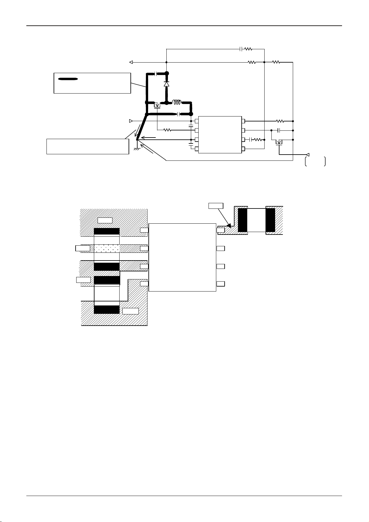
●I/O Equivalent Circuit
OUT (2) VREF (4)
VCC
1.67k
50k
Technical Note
VCC
VCC
INV
GND
OUT
250k
GND
INV (5) FB (6)
20p
200k
CTL/SS (7) RT (8)
200k
193k
~
VREF
~
GND
VCC
FB
GND
VCC
CTL/SS
GND
20k
5k
500k
Fig.12
1k
100k
1k
VREF
RT
GND
www.rohm.com
© 2009 ROHM Co., Ltd. All rights reserved.
8/11
2009.05 - Rev.A

BD9763FVM
Technical Note
●Operation Notes
(1) Absolute maximum ratings
Use of the IC in excess of absolute maximum ratings such as the applied voltage or operating temperature range may
result in IC deterioration or damage. Assumptions should not be made regarding the state of the IC(short mode or open
mode) when such damage is suffered. A physical safety measure such as fuse should be implemented when use of the IC
in a special mode where the absolute maximum ratings may be exceeded is anticipated.
(2) GND potential
Ensure a minimum GND pin potential in all operating conditions. In addition, ensure that no pins other than the GND pin.
Carry a voltage lower then or equal to the GND pin, including during actual transient phenomena.
(3) Thermal design
Use a thermal design that allows for a sufficient margin in light of the power dissipation (Pd) in actual operating conditions.
(4) Inter-pin shorts and mounting errors
Use caution when orienting and positioning the IC for mounting on printed circuit boards. Improper mounting may result in
damage to the IC. Shorts between output pins or between output pins and the power supply and GND pin caused by the
presence of a foreign object may result in damage to the IC.
(5) Operation in a strong electromagnetic field
Use caution when using the IC in the presence of a strong electromagnetic field as doing so may cause the IC to
malfunction.
(6) Thermal shutdown circuit (TSD circuit)
This IC incorporates a built-in thermal shutdown circuit (TSD circuit). The TSD circuit designed only to shut the IC off to
prevent runaway thermal operation.
do not continue to use the IC after operating this circuit or use the IC in an environment where the operation of the thermal
shutdown circuit is assumed.
(7) Testing on application boards
When testing the IC on an application board, connecting a capacitor to pin with low impedance subjects the IC to stress.
Always discharge capacitors after each process or step. Ground the IC during assembly steps as an antistatic measure,
and use similar caution when transporting or storing the IC. Always turn the IC’s power supply off before connecting it to
or removing it from a jig or fixture the inspection process.
(8) Common impedance
Power supply and ground wiring should reflect consideration of the need to lower common impedance and minimize ripple
as much as possible (by making wiring as short and thick as possible or rejecting ripple by incorporating inductance and
capacitance).
(9) Applications with modes that reverse VCC and pin potentials may cause damage to internal IC circuits.
For example, such damage might occur when VCC is shorted with the GND pin while an external capacitor is charged.
It is recommended to insert a diode for preventing back current flow in series with VCC or bypass diodes between VCC
and each pin.
Bypass diode
Back current prevention diode
VCC
Output pin
Fig.13
(10) Timing resistor
Timing resistor connected between RT and GND, has to be placed near RT terminal (8pin).
And pattern has to be short Enough.
www.rohm.com
© 2009 ROHM Co., Ltd. All rights reserved.
9/11
2009.05 - Rev.A

BD9763FVM
Technical Note
(11) IC pin input
This monolithic IC contains P + isolation and PCB layers between adjacent elements in order to keep them isolated.
P/N junctions are formed at the intersection of these P layers with the N layers of other elements to create a variety of
parasitic elements.
For example, when a resistor and transistor are connected to pins as shown in Fig.14,
○the P/N junction functions as a parasitic diode when GND > (Pin A) for the resistor or GND > (Pin B) for
the transistor (NPN).
○Similarly, when GND > (Pin B) for the transistor (NPN), the parasitic diode described above combines
With the N layer of other adjacent elements to operate as a parasitic NPN transistor.
The formation of parasitic elements as a result of the relationships of the potentials of different pins is an inevitable result
of the IC’s architecture. The operation of parasitic elements can cause interference with circuit operation as well as IC
malfunction and damage. For these reasons, it is necessary to use caution so that the IC is not used in away that will
trigger the operation of parasitic elements, such as by the application of voltage lower than the GND (PCB) voltage to input
and output pins.
(Pin A) (Pin B)
+
P
N
P
N
PCB
GND
Parasitic diode
+
P
N
P
N
Parasitic transistors
B
C
+
N
PCB
E
GND
P
N
GND
+
P
N
Other adjacent element
(Pin A)
(Pin B)
GND
B
Parasitic diode
C
E
GND
Parasitic elements
Fig.14
●Power Dissipation Reduction
pd(W)
0.8
0.6
0.4
0.587W
0.2
POWER DISSIPATION : pd(W)
0
25
50
15075 100 1250
175
AMBIENT TEMPERATURE : Ta(℃)
IC mounted on a ROHM standard board (70mm x 70mm x 1.6mm, glass epoxy)
Fig.15
www.rohm.com
© 2009 ROHM Co., Ltd. All rights reserved.
10/11
2009.05 - Rev.A

BD9763FVM
●Ordering part number
B D 9 7 6 3 F V M - T R
Technical Note
Part No.
MSOP8
0.9MAX
Part No.
2.9±0.1
(MAX 3.25 include BURR)
8
2.8±0.1
4.0±0.2
0.75±0.05
0.475
0.08±0.05
1
0.65
2
6
57
4
3
1PIN MARK
+0.05
0.22
–0.04
0.08 S
+
6°
4°
−4°
0.6±0.2
0.29±0.15
+0.05
0.145
–0.03
S
(Unit : mm)
Package
MSOP8
FVM:
<Tape and Reel information>
Embossed carrier tapeTape
Quantity
Direction
of feed
3000pcs
TR
The direction is the 1pin of product is at the upper right when you hold
()
reel on the left hand and you pull out the tape on the right hand
Reel
Packaging and forming specification
TR: Embossed tape and reel
(MSOP8)
1pin
Direction of feed
Order quantity needs to be multiple of the minimum quantity.
∗
www.rohm.com
© 2009 ROHM Co., Ltd. All rights reserved.
11/11
2009.05 - Rev.A

Notes
No copying or reproduction of this document, in part or in whole, is permitted without the
consent of ROHM Co.,Ltd.
The content specied herein is subject to change for improvement without notice.
The content specied herein is for the purpose of introducing ROHM's products (hereinafter
"Products"). If you wish to use any such Product, please be sure to refer to the specications,
which can be obtained from ROHM upon request.
Examples of application circuits, circuit constants and any other information contained herein
illustrate the standard usage and operations of the Products. The peripheral conditions must
be taken into account when designing circuits for mass production.
Great care was taken in ensuring the accuracy of the information specied in this document.
However, should you incur any damage arising from any inaccuracy or misprint of such
information, ROHM shall bear no responsibility for such damage.
The technical information specied herein is intended only to show the typical functions of and
examples of application circuits for the Products. ROHM does not grant you, explicitly or
implicitly, any license to use or exercise intellectual property or other rights held by ROHM and
other par ties. ROHM shall bear no responsibility whatsoever for any dispute arising from the
use of such technical information.
Notice
The Products specied in this document are intended to be used with general-use electronic
equipment or devices (such as audio visual equipment, ofce-automation equipment, communication devices, electronic appliances and amusement devices).
The Products specied in this document are not designed to be radiation tolerant.
While ROHM always makes ef forts to enhance the quality and reliability of its Products, a
Product may fail or malfunction for a variety of reasons.
Please be sure to implement in your equipment using the Products safety measures to guard
against the possibility of physical injury, re or any other damage caused in the event of the
failure of any Product, such as derating, redundancy, re control and fail-safe designs. ROHM
shall bear no responsibility whatsoever for your use of any Product outside of the prescribed
scope or not in accordance with the instruction manual.
The Products are not designed or manufactured to be used with any equipment, device or
system which requires an extremely high level of reliability the failure or malfunction of which
may result in a direct threat to human life or create a risk of human injur y (such as a medical
instrument, transportation equipment, aerospace machinery, nuclear-reactor controller,
fuel-controller or other safety device). ROHM shall bear no responsibility in any way for use of
any of the Products for the above special purposes. If a Product is intended to be used for any
such special purpose, please contact a ROHM sales representative before purchasing.
If you intend to export or ship overseas any Product or technology specied herein that may
be controlled under the Foreign Exchange and the Foreign Trade Law, you will be required to
obtain a license or permit under the Law.
www.rohm.com
© 2009 ROHM Co., Ltd. All rights reserved.
Thank you for your accessing to ROHM product informations.
More detail product informations and catalogs are available, please contact us.
ROHM Customer Support System
http://www.rohm.com/contact/
R0039
A
 Loading...