

Page 1
A
Regulators ICs for Digital Cameras and Camcorders
System Switching Regulator ICs
with Built-in FET (10V)
BD9739KN, BD9740KN
●Description
The 7-channel switching regulators include built-in FETs, and are designed for use in digital still cameras.
They feature built-in power FETs and soft start functionality, reducing the number of external components.
●Features
1) Wide supply voltage range: 1.5 V to 10 V
2) High-precision reference voltage: ± 1%
3) Built-in shutdown circuit for overload (timer-latch type)
4) Oscillator frequency is user-adjustable
5) Built-in thermal shutdown circuit
6) Standby mode current: 0 μA
7) Built-in load switch circuit
8) Selectable step-up/step-down mode
9) Supports inverting circuit for negative output voltage
10) Support a constant-current LED drive for backlight applications
11) Includes multiple synchronous rectification channels
●Applications
Digital still cameras, portable DVD players, and digital video cameras.
●Product lineup
No.10036EAT07
Parameter BD9739KN BD9740KN
Input voltage 1.5 V to 10 V 1.5 V to 10 V
Reference voltage precision 1 V ± 1% 1 V ± 1%
Operating frequency range 100 k to 1.2 MHz 100 k to 1.2 MHz
Step-up 3CH 2CH
Step-down 2CH 1CH
Step-up/step-down switch regulator 1CH 3CH
Inverting 1CH 1CH
Built-in FET 3CH 1CH
Synchronous rectification 3CH 2CH
Load switching 3CH —
Operating temperature range -20℃ to +85℃ -20℃ to +85℃
Package UQFN64 UQFN48
www.rohm.com
© 2010 ROHM Co., Ltd. All rights reserved.
1/14
2010.09 - Rev.
Page 2
A
BD9739KN,BD9740KN
●Absolute maximum ratings
Technical Note
Parameter Symbol
BD9739KN BD9740KN
Ratings
VBAT,VCC,PVCC -0.3 to +12 -0.3 to +12 V
PVCCH,PVCCL -0.3 to +15 -0.3 to +15 V
DRAIN*H, DRAIN*L -0.3 to +12 -0.3 to +12 V
Maximum supply voltage
OUT1B -0.3 to +20 -0.3 to +20 V
OUT2B -0.3 to +17 ― V
SWOUT1,4,PGIN1,PG2,3 -0.3 to +12 ― V
SWIN* -0.3 to +20 ― V
UQFN64 UQFN48
Power dissipation Pd
550
1000
*1-2
*2-2
500
760
Operating temperature range Topr -25~+85 ℃
Storage temperature range Tstg -55~+125 ℃
Junction temperature T
*1: IC without heat sink operation. Reduce by 5.5 mW/℃ (1-2), or 5.0 mW/℃ (1-3) when Ta ≥ 25℃.
*2: When mounted on a PCB (70 mm 70 mm 1.6 mm (thickness), glass epoxy).
Reduced by 10.0 mW/℃ (2-2), or 7.6 mW/℃ (2-3), when Ta ≥ 25℃.
+125 ℃
jmax
●Recommended operating ranges
Parameter Symbol
BD9739KN BD9740KN
Ratings
VBAT 1.5 to 10 1.5 to 10 V
Supply voltage
VCC, PVCC 1.5 to 10 2.8 to 10 V
PVCCL, PVCCH 4.0 to 14 4.0 to 14 V
Parameter Symbol
Min. Typ. Max.
Ratings
Unit Conditions
[Oscillator]
Oscillating frequency f
0.1 — 1.2 MHz
OSC
[Driver block]
DRAIN pin input voltage V
N-channel FET output current
(step-down)
N-channel FET output current
(step-up)
LED channel output current I
Driver output current I
Driver peak current I
Startup NPN TR sink current I
— — 10 V
DRAIN
— — 700 mA
I
OFET1
— — 300 mA
I
OFET2
— — 40 mA
OLED
— — 30 mA External FET drive circuit
OUT
— — 200 mA External FET drive circuit
PEAK
— — 500 mA
NPNSINK
[Positive/negative regulators]
SWOUT1 pin sink current I
PGOUT1 pin source current I
PG23 pin sink current I
SWOUT4 pin source current I
SWOUT6 pin source current I
SWOUT7 pin source current I
— — 10 mA
SWOUT1
— — 100 mA
PGOUT1
— — 1 mA
PG23
— — 50 mA (BD9739KN)
SWOUT4
— — 50 mA
SWOUT6
— — 50 mA
SWOUT7
*1-3
*2-3
Unit
mW
Unit
www.rohm.com
© 2010 ROHM Co., Ltd. All rights reserved.
2/14
2010.09 - Rev.
Page 3
A
BD9739KN,BD9740KN
●Electrical characteristics
(Unless otherwise specified, Ta = 25℃, VBAT = 3 V, VCC = 5 V, RT = 11 k, CT = 180 pF, STB1 to STB7 = 3 V)
Parameter Symbol
Min. Typ. Max.
Limits
Unit Conditions
[Reference voltage, reference voltage for inverting]
Output voltage V
0.99 1.0 1.01 V
REF2
Line regulation DVLI - 4.0 12.5 mV VCC = 3.0 V to 9.5 V
Load regulation DVLO - 1.0 7.5 mV IREF = 10 μA to 100 μA
Output current when shorted IOS 0.2 1 - mA VREF = 0 V
[Internal regulator]
Output voltage REGA V
2.4 2.5 2.6 V IREG = 1 mA
REGA
[Under voltage lockout circuit]
Detection threshold voltage 1 V
Hysteresis width 1 ΔV
Detection threshold voltage 2 V
Hysteresis width 2 ΔV
Detection threshold voltage 3 V
Hysteresis width 3 ΔV
3.45 3.6 3.75 V PVCCL monitor
STD1
- 300 - mV
ST1
2.3 2.4 2.5 V VCC monitor
STD2
- 200 - mV
ST2
- 2.0 - V VREGA monitor
STD3
- 50 - mV
ST3
[Startup circuit block]
Oscillating frequency f
Operation start VBAT voltage V
Soft start charge current I
50 120 220 kHz
START
1.5 - - V VBAT pin monitor
ST1
1.1 2.2 3.3 µA VSS1 = 0 V
SS1
[Short protection circuit ]
Timer threshold voltage VTC 2.1 2.2 2.3 V FB pin monitor
SCP pin source current I
SCP pin detection voltage V
SCP pin standby voltage V
SCP
TSC
SSC
0.5 1.0 1.5 µAVSCP = 0.1 V
2 4 6 (BD9740KN)
0.45 0.50 0.55 V
0.9 1.0 1.1 (BD9740KN)
- 22 170 mV
[Triangular waveform oscillator]
Oscillating frequency f
450 500 550 kHz RT = 11 k, CT = 180 pF
OSC1
Frequency stability Df - 0.3 2 % VCC = 3.0 V to 9.5 V
RT pin voltage VRT 0.78 1.00 1.22 V
[Soft start 23 block] (BD9738KN, BD9739KN)
Soft start charge current I
5 10 15 µA VSS23 = 0 V
SS23
[Error amp]
Low-level output voltage VOL - 1.3 - V INV = 2 V
High-level output voltage VOH V
- 0.3 - - V INV = 0 V
REGA
Output sink current IOI 36 72 - µA FB = 1.7 V, VINV = 1.1 V
Output source current IOO 36 72 - µA FB = 1.7 V, VINV = 0.9 V
DTC pin upper resistance R
DTC pin lower resistance R
NON pin input range I
Non-inverted pin reference volt age V
20 30 40 kΩ (BD9740KN)
DTCU
65 95 125 kΩ (BD9740KN)
DTCD
-0.3 - 1.5 V
RES
- 0.2 - V
NON7
[PWM comparator]
V
- 1.49 - V 0% duty
Input threshold voltage
MAX DUTY D
MAX DUTY (step-up operation) D
T0
V
- 1.95 - V 100% duty
T100
77 85 93 % VINV = 0.9 V, VSCP = 0 V
MAX1
77 85 93 %
MAX2
VINV = 0.9 V,
VSCP, UDSEL = 0 V
[Output circuit]
High-level output voltage V
Low-level output voltage V
High-side N-channel FET
on resistance
Low-side N-channel FET
on resistance
CH7 N-channel FET on
resistance
VCC-1.6 VCC-0.8 - V IO = 30 mA
SATH
- 0.8 1.6 V IO = -30 mA
SATL
R
R
R
ONH
ONL
ONL7
- 270 500 mΩPVCCH = 5 V(IO = 200 mA)
- 300 500 (BD9740KN)
- 270 500 mΩPVCCL = 5 V(IO = 200 mA)
- 300 500 (BD9740KN)
- 0.7 1.4 Ω PVCCL = 5 V(IO = 50 mA)
[Step-up/step-down selector ]
UDSEL pin
control voltage
Note: This IC is not designed to be radiation-resistant.
Step-down V
Step-up V
VCC×0.7 - V
UDDO
0 - VCC×0.3 V
UDUP
V
CC
Technical Note
www.rohm.com
© 2010 ROHM Co., Ltd. All rights reserved.
3/14
2010.09 - Rev.
Page 4
A
BD9739KN,BD9740KN
(Unless otherwise specified, Ta = 25℃, VBAT = 3 V, VCC = 5 V, RT = 11 kΩ, CT = 180 pF, STB1 to STB7 = 3 V)
Parameter Symbol
Min. Typ. Max.
Limits
Unit Conditions
[Power on switching block] (BD9739KN)
SWOUT1
SWOUT4
SWOUT4,6
SWOUT7
Output voltage V
Leak current I
Output voltage V
Leak current I
Output voltage V
Leak current I
Output voltage V
Leak current I
- 0.1 0.3 V IO = 1 mA
SAT
- 0 5 µA STB = 0 V
LEAK
- 0.1 0.3 V IO = 100 μA
SAT
- 0 5 µA STB = 0 V
LEAK
V
SAT
- 0 5 µA STB = 0 V
LEAK
V
SAT
- 0 5 µA STB = 0 V
LEAK
SWIN6
SWIN7
- 0.3 V
- 0.3 V
- 0.1 - V
SWIN6
- 0.1 - V
SWIN7
IO = 20 mA
VSWIN = 5 V
IO = 10 mA
VSWIN = 10 V
[Soft start block] (BD9740KN)
VCC = PVCC = 5V,
mse
Soft start time of CH4 T
Soft start time of CH2, 3 T
CH2, CH3 soft start
INV4 threshold voltage at start
1.8 3.6 6.0
SS1
1.8 3.6 6.0
SS2
V
0.72 0.80 0.88 V
PG4
PVCCH = 5.0V
c
STB 0→3 V
VCC = PVCC = 5V,
mse
STB = 3 V
c
INV4 = 0→1.2 V
VCC = PVCC = 5 V
PVCCH = 5.0 V
[STB1 to STB7]
STB pin control voltage
ON V
OFF V
STB pin pull-down resistance R
2.0 - 11 V STB
STBH
-0.3 - 0.3 V
STBL
250 400 700 kΩ STB
STB
[Circuit current]
Standby current 1
(VBAT pin sink current)
Standby current 2
(VCC, PVCC pin sink current)
Circuit current at startup
(VBAT pin sink current)
Circuit current 1
(VBAT pin sink current)
Circuit current 2
(VCC, PVCC pin sink current)
Note: This IC is not designed to be radiation-resistant.
I
- - 5 µA STB1 to STB7 = 0 V
STB1
- - 5 µA STB1 to STB7 = 0 V
I
STB2
I
- 30 100 mA
ST
- 100 300 µA CT = 1.7 V
I
CC1
I
- 5 15 mA
CC2
CT = 1.7 V
VCC = 0 V
CT = 1.7 V
INV = 2.5 V
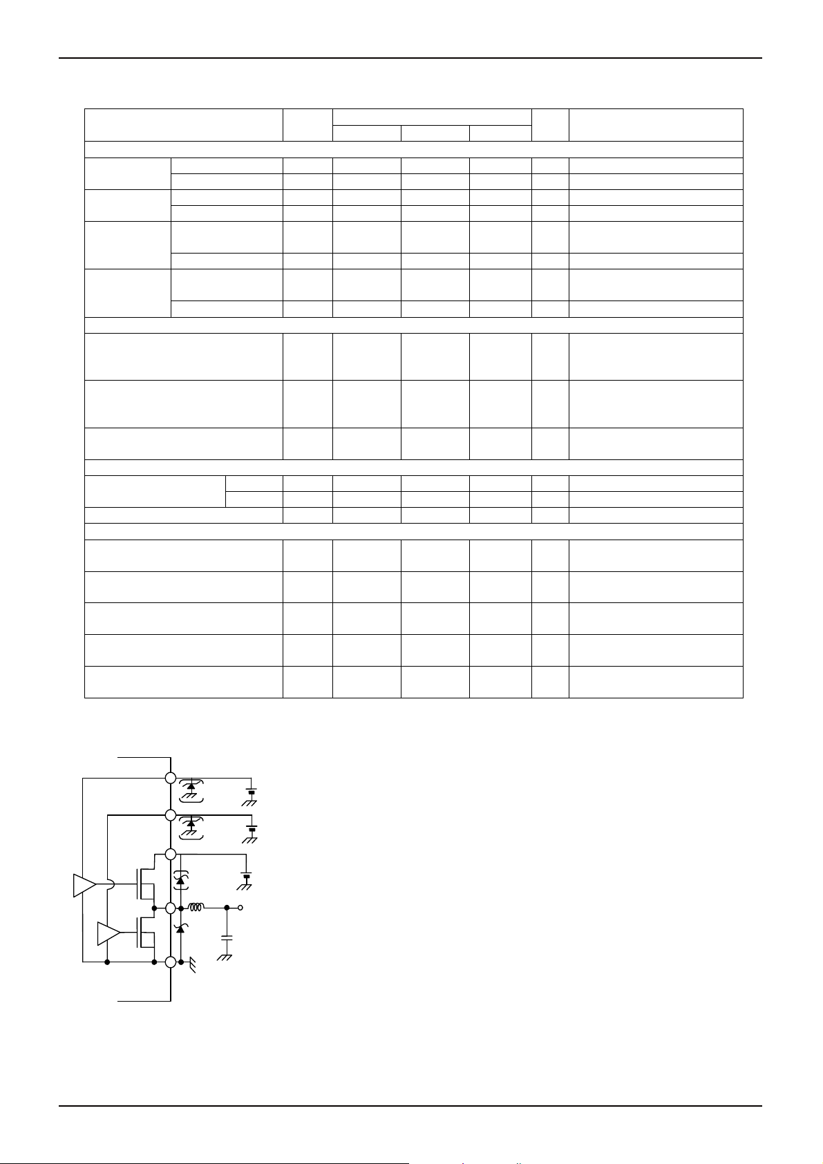
●PVCCH and PVCCL input voltages
PVCCH
Synchronous rectification channels with built-in FETs include, N-channel FETs
for both the high-side and low-side configuration. The driver block's power
source is supplied to the PVCCL pin for the low-side and the PVCCH pin for
PVCCL
the high-side. (For the BD9740KN, both sides are supplied to the PVCCH pin.)
In order to turn the FET on, a potential of at least 4 V must be supplied to the
DRAINH
PVCCL pin, and a potential of at least, DRAINH pin voltage + 4 V, must be
supplied to the PVCCH pin.
Note:
DRAINL
The breakdown voltage for the PVCCL and PVCCH pins is 15 V.
For applications that with voltages exceeding 15 V, add a zener diode, or other
Vo
components, to provide overvoltage protection.
Shorting the DRAINH pin with the ground, while a charge remains in the output
capacitor, may cause unexpected current flow, resulting in damage to the IC.
PGND
Add an external protective diode for applications where this possibility exists.
Fig. 1 Synchronous Rectification
Channel with Built-In FET
Technical Note
www.rohm.com
© 2010 ROHM Co., Ltd. All rights reserved.
4/14
2010.09 - Rev.
Page 5
A
BD9739KN,BD9740KN
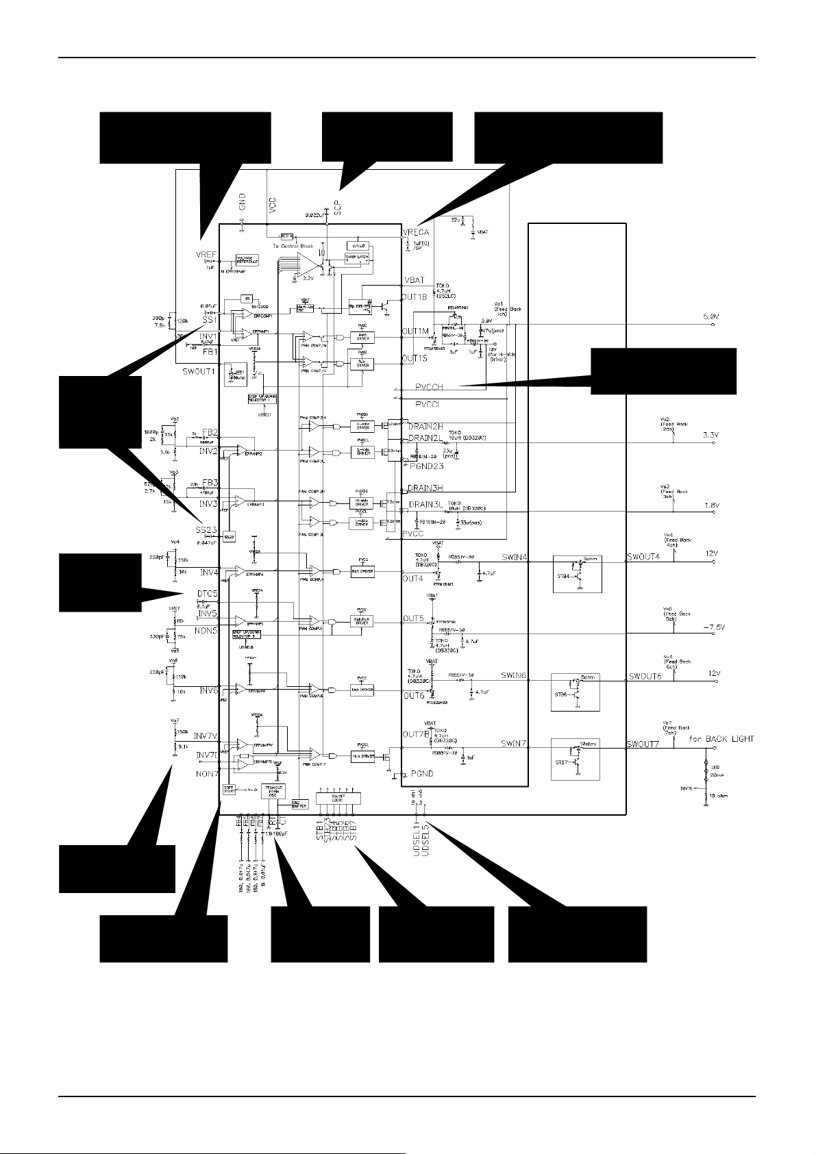
●Block diagram and application circuit (BD9739KN)
Connect a capacitor to prevent
oscillation to the VREF pin.
(See page 7.)
For more information
about setting the SCP pin,
(See page 7.)
Connect a
capacitor for setting
the soft star t time .
(See pages 8& 9.)
Connect a
capacitor for soft
start at DTC pin.
(See page 8.)
Connect a resistor for
setting the output voltage.
(See page 8.)
The soft start times for CH4,
6, 7 are fixed internally.
(See page 9.)
Set the operating
frequency with the
RT and CT pins.
(See page 8.)
Connect a capacitor to prevent
oscillation to the VREGA pin.
(See page 7.)
Set whether CH1 and CH5
will be used as step-up,
step-down or inversion.
(See page 7.)
This pin is used as the
on/off control pin.
(See page 7.)
Fig. 2 BD9739KN Application Circuit
Technical Note
Apply the PVCCH pin voltage
with an external charge
pump. (See page 4.)
www.rohm.com
© 2010 ROHM Co., Ltd. All rights reserved.
5/14
2010.09 - Rev.
Page 6

A
BD9739KN,BD9740KN
(
)
pag
(
)
(
)
(
)
●Block diagram and application circuit (2) BD9740KN
Connect a capacitor to prevent
oscillation to the VREF pin.
(See page 7.)
For more information
about setting the SCP pin,
see
Connect a capacitor
for setting the soft
start time.
(See page 8&9.)
The soft start times
for CH2 to CH4 are
fixed internally.
(See page 9.)
Connect a capacitor
for soft start at TC
pin.
(See page 8.)
Connect a resistor for
setting the output
voltage. (See page 8.)
Set the operating frequency
with the RT and CT pins.
See page 8.
Fig. 3 BD9740KN Application Circuit
e 7.
Connect a capacitor to prevent
oscillation to the VREGA pin.
See page 7.
This pin is used as the
on/off control pin.
See page 7.
Technical Note
Apply the PVCCH pin voltage
with an external charge pump.
(See page 4.)
Set whether CH1, CH2, and CH3 will be
used as step-up or step-down.
See page 7.
www.rohm.com
© 2010 ROHM Co., Ltd. All rights reserved.
6/14
2010.09 - Rev.
Page 7

A
BD9739KN,BD9740KN
●BD9739KN Pin No.
Pin No. Pin name Pin No. Pin name Pin No. Pin name
61 VBAT 60 OUT1B 44,36 NON5,7
29 VCC 4,5,12,13 DRAIN2,3H 28 SS1
54 PVCC 6,7,10,11 DRAIN2,3L 25 SS23
14 PVCCH 55 OUT1M 34 RT
59 PVCCL 56 OUT1S 33 CT
8,9,57 PGND23,PGND 35 VREF 32 SCP
42 GND 43 DTC 5 1,64 UDSEL1,5
30 VREGA 26,24,21,47,46,41,39 FB 1~7 15,16,17,18,19,20 STB 1,23,4,5,6,7
51,52,53 OUT4,5,6 27,23,22,48,45,40 INV 1~6 50,2,62 SWIN4,6,7
58 OUT7B 37,38 INV7I,INV7V 31,49,3,63 SWOUT 1,4,6,7
●BD9740KN Pin No.
Pin No. Pin name Pin No. Pin name Pin No. Pin name
4 VBAT 44 MAIN2 30,37 NON6,NON7
21 VCC 43 SUB2 17 SS1
46 PVCC 5 OUT1B 23 RT
10 PVCCH 9 DRAIN4H 24 CT
42 PGND 8 DRAIN4L 25 SCP
6,7 PGND4 20 VREF 1 UDSEL12
31 GND 3,38,39 DTC 5~7 2 UDSEL3
22 VREGA 16,18,27,28,32,35,36 FB 1~7 11,12,13,14 STB1,234,56,7
40,41,45,47,48 OUT1,3,5,6,7 15,19,26,29,33,34 INV 1~5,7
●Block diagram explanation and setting periphera l IC components
1. Voltage reference (VREF)
VREF is the reference voltage source of 1.0V output voltage.
Connect a capacitor to prevent oscillation. Set the capacitance from 1.0 μF to 10 μF.
2. REGA
REGA and REGD are regulators with output voltages of 2.5 V. REGA is used as the power supply for the IC's internal
blocks.Connect a capacitor to prevent oscillation. Set the capacitance from 4.7 μ to 10 μF.
3. UDSEL
To enable step-up mode, connect VCC to the UDSEL pin. To enable step-up mode connect 0V to the UDSEL pin.
When using the startup circuit, set the pin to step-up mode. Because the pin uses COMS inverter input, you must connect
the pin to either GND or VCC in order to prevent undefined input.
4. On/off logic
The voltage applied to the STB pins can be controlled whether each channel is on or off.
CH1, CH4, and CH5 can be controlled independently, while CH2 and CH3 can be controlled simultaneously.
Applying a voltage of over 2 V turns on the corresponding channel(s), while leaving the pin open or app lying 0 V turns off
the corresponding channel(s).
Turning off all channels causes the IC to be in a standby state.
Each pin is connected to GND by a 400 k pull-down resistor.
5. Setting the short protection detection time
The detection time can be set when the capacitor is connected to the SCP pin.
When the detection time is reached, the latch circuit operates, turning off the output for all channels.
To reset the latch circuit, turn all STB pins off, and then back on again.
Detection time (sec) = CSCP VTSC / ISCP
(CSCP: capacitance; VTSC: SCP pin detection voltage, ISCP: SCP pin source current)
*Set the capacitor that is connected to the SCP pin from 0.001 μF to 2.2 μF.
Technical Note
www.rohm.com
© 2010 ROHM Co., Ltd. All rights reserved.
7/14
2010.09 - Rev.
Page 8

A
BD9739KN,BD9740KN
Technical Note
6. Setting the oscillating frequency
The oscillating frequency can be set by connecting the res istance value to the RT pin and connecting the capacitance
value to the CT pin.
Oscillating frequency = VRT / (CT RT) (Unit: Hz)
*Set the resistance value, connected to the RT pin, from 4.7 k to 30 k
*Set the capacitance value, connected to the CT pin, from 100 pF to 10,000 pF.
(VRT: RT pin voltage; CT: OSC timing capacitance; RT: OSC timing resistance)
1000
1000
OSCILATING FREQUENCY [kHz]
100
10
RT pin RESISTANCE[k]
Fig. 4 Oscillating Frequency Versus RT Pin Resistance
100pF
180pF
330pF
100
11kΩ
20kΩ
30kΩ
100
OSCILATING FREQUENCY: fosc [kHz]
100
CT pin CAPACITANCE [pF]
1000
Fig. 5 Oscillating Frequency Versus CT Pin Capacitance
7. Startup channel soft-start operation
The startup channel's soft start can be controlled by the capacitor connected to the SS1 pin.
Times can be determined with the following equation:
Startup time (sec) = (VSS / ISS) CSS
(VSS = SS pin voltage [= 0.7 V], ISS = soft start charge current [= approximately 2.0 μA]; CSS = capacitor capacitance)
Example: When CSS = 0.01 μF, startup time = 0.7 / (2.0 10-6) (0.01 10-6) = 3.5 ms
*Set the capacitance value, connected to the SS1 pin, from 0.001 μF to 2.2 μF.
VCC output voltage waveform
STBY1
SS1
(Startup block repeat
oscillation prohibited)
(Startup block Main)
Approximately
0.5 V
Approximately 1.0 V
Approximately 0.7 V
OSC
VCC
VREGA
SS pin voltage
waveform
Fig. 6 Startup Channel Startup Waveform
(Reference Data)
VCC
VREGA
OUT1B
DRAIN1L
Startup OSC
(approximately 100 kHz)
VREF=1.0 V
Fig. 7 Timing Chart
8. SWOUT1 pin (BD9734KN/BD9738KN/BD9739KN)
To prevent current from flowing from VOUT1 to the feedback resistor, during standby operation, connect the ground side of
CH1's feedback resistor to SWOUT1.
9. Soft start operation depending on SS pins (BD9739KN)
Soft start operation for CH2 and CH3 can be controlled by the capacitor connected to the SS23 pins.
Times can be determined with the following equation:Startup time (sec) = (VSS / ISS) CSS23
(VSS: SS pin voltage [= 1.0 V]; ISS: soft start charge current [= approximately 10 μA]; CSS: capacitance)
*Startup of CH2 begins when CH3 output reaches approximately 70%.
*Set the capacitance value, connected to each SS23 pin, from 0.005 μF to 1.0 μF.
VREGA
RA
RB
DTC
Fig. 8 DTC External Setting Circuit
VREGA
R1
R2
Approximately
30 k
Approximately
93 k
FB
www.rohm.com
© 2010 ROHM Co., Ltd. All rights reserved.
8/14
2010.09 - Rev.
Page 9

A
BD9739KN,BD9740KN
10. Setting MAX DUTY
The DTC voltage is determined by the internal R1 and R2 resistance values. The DTC voltage can be changed by
connecting resistance values that are from 1 to 2 digits smaller than the internal R1 (30 k) and R2 (93 k) resistors, to
the RA and RB pins.
*The resistors connected to the RA and RB pins should be at least 5 k. Avoid shorting the VREGA and DTC pins.
*When VCC falls to 2.8 V or below, a protection circuit will operate to limit MAX DUTY in order to prevent the IC from
malfunctioning when VREGA (the internal circuit power supply) drops.
11. Soft start operation triggered by the DTC pin
Soft start operation can be set by connecting a capacitor to the DTC pin. Setting the STBY pin to high will cause the
capacitor connected to the DTC pin to be charged by the internal pull-up resistor.
Startup will begin when this voltage reaches the minimum voltage of the CT pin's triangular waveform.
*Set the capacitance connected to each DTC pin to 10 μF or less.
12. Internal soft start operation
Soft start times are set internally for CH4, CH6, and CH7 (BD9739KN); and CH2 to CH4 (BD9740KN).
BD9739KN CH4, 6, 7: 2.7 ms
BD9740KN CH2 to CH4: 3.6 ms
(Soft start operation of CH2 and CH3 is delayed until CH4 reaches approximately 80%.)
13. Setting the error amp feedba ck resistance
(1) Feedback resistance order (BD9739KN, BD9740KN)
Error amp differential input is formed by a PNP transistor, with the base current of this input flowing into the lower
voltage divider resistor. In the worst case, this current may reach 0.2 μA. For this reason, when the resistance of the
lower resistor is increased, the base current may cause an error in the output voltage. For example, resistance values
of 40 k, 20 k, and 10 k result in errors of 1%, 0.5%, and 0.25%, respectively. Refer to these values when setting
the resistance value.
(2) Setting the inverted channel (BD9739KN, BD9740KN)
For the BD9739KN, connect the CH5 error amp reference voltage (INV5) to the ground.
For the BD9740KN, the CH6 error amp reference voltage is grounded internally.
*It is recommended to use a 10 k resistor between VREF and CH5 output. Use a resistance value from 5 k to 20 k.
Technical Note
www.rohm.com
© 2010 ROHM Co., Ltd. All rights reserved.
9/14
2010.09 - Rev.
Page 10

A
BD9739KN,BD9740KN
●I/O Equivalent circuit diagrams
DTC5 to DTC7
(dead time control)
DTC6
DTC7
Vcc DTC5
VREGA
SS1 (startup channel soft start
capacitor connection pin)
VBAT
Vcc
Vcc
SS1
CT (triangular waveform timing
capacitance connection)
VREGA
Vcc
CT
VREF (reference voltage output)
Vcc
Vcc
Vcc
VREF
Vcc
INV2 to INV6, INV7 V
(error amp inverted input)
Vcc
INV2 to INV6,
INV7V
INV7I (error amp inverted input)
NON7 (error amp non-inverted input)
Vcc
INV7I
NON7
SCP (timer latch time setting
capacitor connection pin)
VREGA
Vcc
SCP
DELAY (POWERGOOD
time constant setting pin)
Vcc
VREGA
Vcc
DELAY
Fig. 9 I/O Equivalent Circuit Diagrams (1)
VREGA
VREF
Technical Note
INV1
(error amp inverted input)
Vcc
INV1
RT (triangular waveform timing
resistor connection)
VREGA (REGA output)
Vcc
UDSEL (step-up/step-down select input)
UDSEL1 to
UDSEL 5
Vcc
Vcc
VREGA
Vcc
Vcc
VREGA
Vcc
RT
www.rohm.com
© 2010 ROHM Co., Ltd. All rights reserved.
10/14
2010.09 - Rev.
Page 11

A
BD9739KN,BD9740KN
STBY1 to STBY7 (CH1 to CH7 on/off control)
REGON (CCD REG control input)
MODE (CCD sequence control pin)
STBY1 to STBY7
REGON
MODE
SWIN (load switch input pin)
SWOUT (load switch output pin)
SWIN4, 6, 7
SWOUT4, 6, 7
PG1IN (POWERGOOD 1 input)
PG1OUT (POWERGOOD
switch 1 output)
PG1IN
PVCCH
PG1OUT
OUT6 (power transistor connection)
PVCC (power supply input)
PGND4 (power ground)
VCC
Vcc
PVCC
OUT6
Vcc
PGND4
Vcc
FB (error amp output)
Vcc
FB1 to FB7
DRAIN1, 2, 3H
(power MOS drain for CH1, CH2, and CH3)
DRAIN1, 2, 3L
(power MOS drain for CH1, CH2, and CH3)
PGND1, 23 (output step ground)
DRAIN1,2,3H
Vcc
VBAT2 (battery input [dri ver block])
OUT1B (CH1 power transistor collector output)
Fig. 10 I/O Equivalent Circuit Diagrams (2)
DRAIN1,2,3L
PGND1,23
VBAT2
OUT1B
7CH (power transistor drain output)
Vcc
PGND4
SYNC_DTC (synchronous
rectificati on de lay time setting pin)
SYNC_DT
C
MAIN4 (CH4 main output)
SUB4 (CH4 sub output)
OUT5 (power transistor connection)
SWOUT1, 4 (load switch output pin)
PG23 (POWERGOOD switch 23 output)
SS2 (soft start capacitor connection pin)
SS2
Technical Note
OUT7B
VREGA
Vcc
Vcc
Vcc
Vcc
SWOUT1, 4
PG23
VREGA
Vcc
PVCC
MAIN4
SUB4
OUT5
PGND4
www.rohm.com
© 2010 ROHM Co., Ltd. All rights reserved.
11/14
2010.09 - Rev.
Page 12

A
BD9739KN,BD9740KN
●Notes for use
1) Absolute maximum ratings
An excess in the absolute maximum ratings, such as supply voltage, temperature range of operating conditions, etc., can
break down the devices, thus making impossible to identify breaking mode, such as a short circuit or an open circuit. If any
over rated values will expect to exceed the absolute maximum ratings, consider ad ding circuit protection devices, such as
fuses.
2) Reverse polarity co nnection of the power supply
Connecting the of power supply in reverse polarity can damage IC. Take precautions when connecting the power supply
lines. An external direction diode can be added.
3) Power supply lines
Design PCB layout pattern to provide low impedance GND and supply lines. To obtain a low noise ground and supply line,
separate the ground section and supply lines of the digital a nd analog bl ocks. F urthermore, for all p ower supply termina ls
to ICs, connect a capacitor between the power supply and the GND terminal. When applying electrolytic capacitors in the
circuit, note that capacitance characteristic values are reduced at low temperatures.
4) GND voltage
Ground-GND potential should maintain at the minimum ground voltage level. Furthermore, no terminals should be l ower
than the GND potential voltage including an electric transients.
5) Thermal design
Use a thermal design that allows for a sufficient margin in light of the power dissipation (Pd) in actual operating conditions.
6) Inter-pin shorts and mounting errors
Use caution when positioning the IC for mounting on printed circuit boards. The IC may be damaged if there is any
connection error or if positive and ground power supply terminals are reversed. The IC may also be damaged if pins are
shorted together or are shorted to other circuit’s power lines.
7) Operation in a strong electromagnetic field
Use caution when using the IC in the presence of a strong electromagnetic field as doing so may cause the IC to
malfunction.
8) ASO
When using the IC, set the output transistor so that it does not exceed absolute maximum ratings or ASO.
9) Thermal shutdown circuit (TSD circuit)
The IC incorporates a built-in thermal shutdown circuit (TSD circuit). The thermal shutdown circuit (TSD circuit) is
designed only to shut the IC off to prevent runaway thermal operation. It is not designed to protect the IC or guar antee its
operation. Do not continue to use the IC after operating this circuit or use the IC in an environment where the operation of
this circuit is assumed.
10) Capacitors connected between output and ground pins
If a large capacitance value is connected between the output and ground pins, and if the VCC falls to 0 V or becomes
shorted with the ground pin, the current stored in the capacitor may flow to the output pin. This can cause damage to the
IC. Set capacitors connected between the output and ground pins to values that fall within the recommended range.
11) Testing on application boards
When testing the IC on an application board, connecting a capacitor to a pin with low impedance subjects the IC to stress.
Always discharge capacitors after each process or step. Always turn the IC's power supply off before connecting it to, or
removing it from a jig or fixture, during the inspection process. Ground t he IC during assembly steps as an antistatic
measure. Use similar precaution when transporting and storing the IC.
12) Reg arding input pin of the IC (Fig 11)
This monolithic IC contains P
junctions are formed at the intersection of these P layers with the N layers of other elements, creating a parasitic diode or
transistor. For example, the relation between each potential is as follows:
When GND > Pin A and GND > Pin B, the P–N junction operates as a parasitic diode.
When Pin B > GND > Pin A, the P–N junction operates as a parasitic transistor.
Parasitic diodes can occur inevitably in the structure of the IC. The operation of parasitic diodes can result in mut ual
interference among circuits, operational faults, or physical damage. Accordingly, methods by which parasitic diodes
operate, such as applying a voltage that is lower than the GND (P substrate) voltage to an input pin, should not be used.
+
isolation and P substrate layers between adjacent elements to keep them isolated. P–N
Technical Note
www.rohm.com
© 2010 ROHM Co., Ltd. All rights reserved.
12/14
2010.09 - Rev.
Page 13

A
BD9739KN,BD9740KN
(
13) Ground wiring patterns
The power supply and ground lines must be as short and thick as possible to reduce line impedanc e. Fluctuating voltage
on the power ground line may damage the device.
14) STB pin voltage
Set the STB pin voltage to 0.3 V or lower when setting channels to a standby state, or to 2.0 V or higher when setting
channels to an operational state. Do not lengthen transition times or fix the STB pin voltage to values h igher than 0.3 V or
lower than 2.0 V. Doing so may cause the IC to malfunction.
15) Common supply voltage
Use a common supply voltage for both the driver block and the main block. The IC is not compatible with applications
requiring the driver block to be used while applying user-selected voltages.
16) Setting the MAX DUTY
MAX DUTY limitations may not operate when using the IC at high frequencies. When using the IC in such applications ,
allow for sufficient margins when setting external components.
(Pin A)
N
Resistor
PCB
P
N
Parasitic elements
(Pin B)
P+ P+
N
Parasitic elements
Fig. 11 Example of Simple Bipolar IC Architecture
Transistor (NPN)
C
+
P
N
B
N
N
PCB
~
~
P
GND
E
(Pin B)
GND
+
P
N
Other Adjacent
Elements
Pin A)
Technical Note
C
B
~
~
E
GND
Parasitic elements
GND
~
~
Parasitic
elements
www.rohm.com
© 2010 ROHM Co., Ltd. All rights reserved.
13/14
2010.09 - Rev.
Page 14

A
BD9739KN,BD9740KN
●Ordering part number
B D 9 7 3 9 K N - E 2
Part No.
Part No.
9739
9740
UQFN64
8.2±0.1
8.0±0.1
(1.1)
48 33
0.2±0.05
32
17
161
M
0.05
0.02
-
+0.03
0.02
0.95MAX
0.05
4−(0.35)
Notice :
Do not use the dotted line area
for soldering
(0.2)
0.4
(Unit : mm)
49
8.0±0.1
8.2±0.1
64
0.22±0.05
+0.1
0.6
-
0.3
UQFN48
(1.4)
7.2± 0.1
0.6
(0.55)
7.0± 0.1
+0.1
-
0.22± 0.05
0.3
7.2± 0.1
7.0± 0.1
36
25
1
0.2± 0.05
0.4
24
13
12
M
0.05
0.02
-
+0.03
0.95MAX
0.02
0.05
3-(0.45)
Notice :
Do not use the dotted line area
(0.2)
for soldering
(Unit : mm)
37
48
Package
KN: UQFN64
UQFN48
<Tape and Reel information>
Embossed carrier tape (with dry pack)Tape
Quantity
Direction
of feed
<Tape and Reel information>
Quantity
Direction
of feed
2500pcs
E2
The direction is the 1pin of product is at the upper left when you hold
()
reel on the left hand and you pull out the tape on the right hand
Reel
1pin
Embossed carrier tape (with dry pack)Tape
2500pcs
E2
The direction is the 1pin of product is at the upper left when you hold
()
reel on the left hand and you pull out the tape on the right hand
Reel
1pin
Packaging and forming specification
E2: Embossed tape and reel
Order quantity needs to be multiple of the minimum quantity.
∗
Order quantity needs to be multiple of the minimum quantity.
∗
Technical Note
Direction of feed
Direction of feed
www.rohm.com
© 2010 ROHM Co., Ltd. All rights reserved.
14/14
2010.09 - Rev.
Page 15

Notes
No copying or reproduction of this document, in part or in whole, is permitted without the
consent of ROHM Co.,Ltd.
The content specied herein is subject to change for improvement without notice.
The content specied herein is for the purpose of introducing ROHM's products (hereinafter
"Products"). If you wish to use any such Product, please be sure to refer to the specications,
which can be obtained from ROHM upon request.
Examples of application circuits, circuit constants and any other information contained herein
illustrate the standard usage and operations of the Products. The peripheral conditions must
be taken into account when designing circuits for mass production.
Great care was taken in ensuring the accuracy of the information specied in this document.
However, should you incur any damage arising from any inaccuracy or misprint of such
information, ROHM shall bear no responsibility for such damage.
The technical information specied herein is intended only to show the typical functions of and
examples of application circuits for the Products. ROHM does not grant you, explicitly or
implicitly, any license to use or exercise intellectual property or other rights held by ROHM and
other parties. ROHM shall bear no responsibility whatsoever for any dispute arising from the
use of such technical information.
Notice
The Products specied in this document are intended to be used with general-use electronic
equipment or devices (such as audio visual equipment, ofce-automation equipment, communication devices, electronic appliances and amusement devices).
The Products specied in this document are not designed to be radiation tolerant.
While ROHM always makes efforts to enhance the quality and reliability of its Products, a
Product may fail or malfunction for a variety of reasons.
Please be sure to implement in your equipment using the Products safety measures to guard
against the possibility of physical injury, re or any other damage caused in the event of the
failure of any Product, such as derating, redundancy, re control and fail-safe designs. ROHM
shall bear no responsibility whatsoever for your use of any Product outside of the prescribed
scope or not in accordance with the instruction manual.
The Products are not designed or manufactured to be used with any equipment, device or
system which requires an extremely high level of reliability the failure or malfunction of which
may result in a direct threat to human life or create a risk of human injury (such as a medical
instrument, transportation equipment, aerospace machinery, nuclear-reactor controller, fuelcontroller or other safety device). ROHM shall bear no responsibility in any way for use of any
of the Products for the above special purposes. If a Product is intended to be used for any
such special purpose, please contact a ROHM sales representative before purchasing.
If you intend to export or ship overseas any Product or technology specied herein that may
be controlled under the Foreign Exchange and the Foreign Trade Law, you will be required to
obtain a license or permit under the Law.
Thank you for your accessing to ROHM product informations.
More detail product informations and catalogs are available, please contact us.
ROHM Customer Support System
www.rohm.com
© 2010 ROHM Co., Ltd. All rights reserved.
http://www.rohm.com/contact/
R1010
A
 Loading...