

Page 1

Hi-performance Regulator IC Series for PCs
FET Integrated
Switching Regulator for DDR-SDRAM Cores
BD95514MUV
●Description
BD95514MUV is a switching regulator capable of supplying high current output (up to 4A) at low output voltages (0.7V~5.0V)
over a broad range of input voltages (4.5V~28V). The regulator features an internal N-MOSFET power transistor for high
efficiency and low space consumption, while incorporating ROHM’s proprietary H
the industry’s fastest transient response time against load changes. SLLM (Simple Light Load Mode) technology is also
integrated to improve efficiency when powering lighter loads, as well as soft start, variable frequency, short-circuit protection
with timer latch, over-voltage protection, and REF tracking functions. This regulator is suited for PC applications.
●Features
1) I Internal low ON-resistance power N-MOSFET (typ:120m)
2) I Internal 5V linear voltage regulator (100mA)
3) Integrated H
4) Selectable Simple Light Load Mode (SLLM), Quiet Light Load Mode (QLLM) and forced continuous mode
5) Built-in thermal shutdown, low input, current overload, output over- and under-voltage protection circuitry
6) Soft start function to minimize rush current during startup
7) Adjustable switching frequency (f = 200 kHz ~ 1000 kHz:It changes depending on the setup condition.)
8) Built-in output discharge function
9) VQFN032V5050 power package
10) Tracking function
11) Internal bootstrap diode
●Applications
Mobile PCs, desktop PCs, LCD-TV, digital household electronics
3
RegTM DC/DC converter controller
3
Reg
TM
control mode technology, yielding
No.09030EBT16
www.rohm.com
© 2009 ROHM Co., Ltd. All rights reserved.
1/15
2009.04 - Rev.B
Page 2
BD95514MUV
Technical Note
●Absolute Maximum Ratings (Ta=25°C)
Parameter Symbol Value Unit
Input Voltage 1 VCC 7 *1 V
Input Voltage 2 VDD 7
*1
V
Input Voltage 3 AVIN 30 *1
Input Voltage 4 VIN 30 *1 V
External VCC Voltage EXTVCC 7 *1 V
BOOT Voltage BOOT 35 V
BOOT-SW Voltage BOOT-SW 7 *1 V
Output Feedback Voltage FB VCC V
SS/FS/MODE Voltage SS/FS/MODE VCC V
VREG Voltage VREG VCC V
EN/CTL Input Voltage EN/CTL 7 *1 V
PGOOD Voltage PGOOD 7 *1 V
Output Current (Average) Isw 4 *1 A
Power Dissipation 1 Pd1 0.38*2 W
Power Dissipation 2 Pd2 0.88
Power Dissipation 3 Pd3 2.06
Power Dissipation 4 Pd4 4.56
*3*6
W
*4*6
W
*5*6
W
Operating Temperature Range Topr -10~+100 °C
Storage Temperature Range Tstg -55~+150 °C
Junction Temperature Tjmax +150 °C
*1 Do not exceed Pd.
*2 Ta≧25°C (IC only), power dissipated at 3.0mW / °C.
*3 Ta≧25°C (single-layer board, 20.2 mm
*4 Ta≧25°C (4-layer board, 10.29 mm
*5 Ta≧25°C (4-layer board, all layers with 5505 mm
*6 Values observed with chip backside soldered. When unsoldered, power dissipation is lower.
2
copper heat dissipation pad), power dissipated at 7.0mW / °C.
2
copper heat dissipation pad on top layer, 5505 mm2 pad on 2nd and 3rd layer), power dissipated at 16.5mW / °C.
2
copper heat dissipation pads), power dissipated at 36.5mW / °C.
●Operating Conditions (Ta=25°C)
Parameter Symbol Min Max Unit
Input Voltage 1 VCC 4.5 5.5 V
Input Voltage 2 VDD 4.5 5.5 V
Input Voltage 3 AVIN 4.5 28 V
Input Voltage 4 VIN 4.5 28 V
External VCC Voltage EXTVCC 4.5 5.5 V
BOOT Voltage BOOT 4.5 33 V
SW Voltage SW -0.7 28 V
BOOT-SW Voltage BOOT-SW 4.5 5.5 V
MODE Input Voltage MODE 0 5.5 V
EN/CTL Input Voltage EN/CTL 0 5.5 V
PGOOD Voltage PGOOD 0 5.5 V
Minimum On Time tonmin - 100 nsec
*This product is not designed for use in a radioactive environment.
www.rohm.com
© 2009 ROHM Co., Ltd. All rights reserved.
2/15
2009.04 - Rev.B
Page 3
BD95514MUV
●ELECTRICAL CHARACTERISTICS
(unless otherwise noted, Ta=25℃, AVIN=12V, VCC=VDD=VREG, EN/CTL=5V, MODE=0V, RFS=180kΩ)
Parameter Symbol
[Whole Device block]
AVIN bias current 1 IIN1 - 1300 2000 A
AVIN bias current 2 IIN2 - 200 300 A EXTVCC=5V
AVN standby current IINstb - 0 10 A CTL=EN=0V
EN Low voltage ENlow GND - 0.8 V
EN High voltage ENhigh 2.3 - 5.5 V
EN bias current IEN - 12 20 A
CTL Low voltage CTLlow GND - 0.8 V
CTL High voltage CTLhigh 2.3 - 5.5 V
CTL bias current ICTL - 1 6 A
[5V Linear regulator block ]
VREG output voltage VREG 4.90 5.00 5.10 V AVIN=6.0 to 25VIREG=0 to 100mA
Maximum current IREG 200 - - mA
[5V switch block ]
EXTVCC input threshold voltage EVCC_UVLO 4.2 4.4 4.6 V EXTVCC:Sweep up
Switch resistance REVCC - 1.0 2.0
[Under Voltage Locked Out block ]
AVIN threshold voltage AVIN_ UVLO 4.1 4.3 4.5 V VCC:Sweep up
AVIN hysteresis voltage dAVIN_ UVLO 100 160 220 mV VCC:Sweep down
VREG threshold voltage VREG_ UVLO 4.1 4.3 4.5 V VREG:Sweep up
VREG hysteresis voltage dVREG_ UVLO 100 160 220 mV VREG:Sweep down
[H3RegTM block]
ON Time ton 400 500 600 nsec
MAX ON Time tonmax 5.0 11.0 22.0 sec
MIN OFF Time toffmin - 450 550 nsec
[FET Driver block]
High side ON resistance Ron_high - 120 200 m
Low side ON resistance Ron_low - 120 200 m
[SCP block]
SCP startup voltage VSCP 0.420 0.490 0.560 V VFB:30%down
Delay time tSCP 0.5 1 2 ms
[OVP block]
OVP setting voltage VOVP 0.800 0.840 0.880 V VFB:20%up
Delay time tOVP 0.5 1 2 ms
[Soft start block]
Charge current Iss 1.4 2.2 3.0 A
Standby voltage Vss_stb - - 100 mV
[Current Limit block]
High side FET output current limit IHOCP 4.5 6.0 7.5 A High peak detect
Low side FET output current limit ILOCP 3.0 4.0 5.0 A Low peak detect
[Output Voltage Sense block]
Feedback pin voltage 1 VFB1 0.693 0.700 0.707 V
Feedback pin voltage 2 VFB2 0.690 0.700 0.710 V Ta=-10℃ to 100℃,Iout=0A to 4A
Feedback pin bias current IFB -100 0 100 nA
[Mode block]
SLLM VthSLLM VCC-0.5 - VCC V SLLM(Maximum LG offtime:∞)
Forced continuous mode VthCONT GND - 0.5 V Continuous mode
QLLM VthQLLM 2.5 3.0 3.5 V QLLM(Maximum LG offtime:40usec)
Open voltage VMODE 1.5 - 3.0 V
[Power Good block]
VFB Power Good Low voltage VFB PL 0.605 0.630 0.655 V VFB:10%down
VFB Power Good High voltage VFB PH 0.745 0.770 0.795 V VFB:10%up
Standard Value
MIN TYP MAX
Unit Condition
Technical Note
www.rohm.com
© 2009 ROHM Co., Ltd. All rights reserved.
3/15
2009.04 - Rev.B
Page 4
BD95514MUV
T
T
T
T
Technical Note
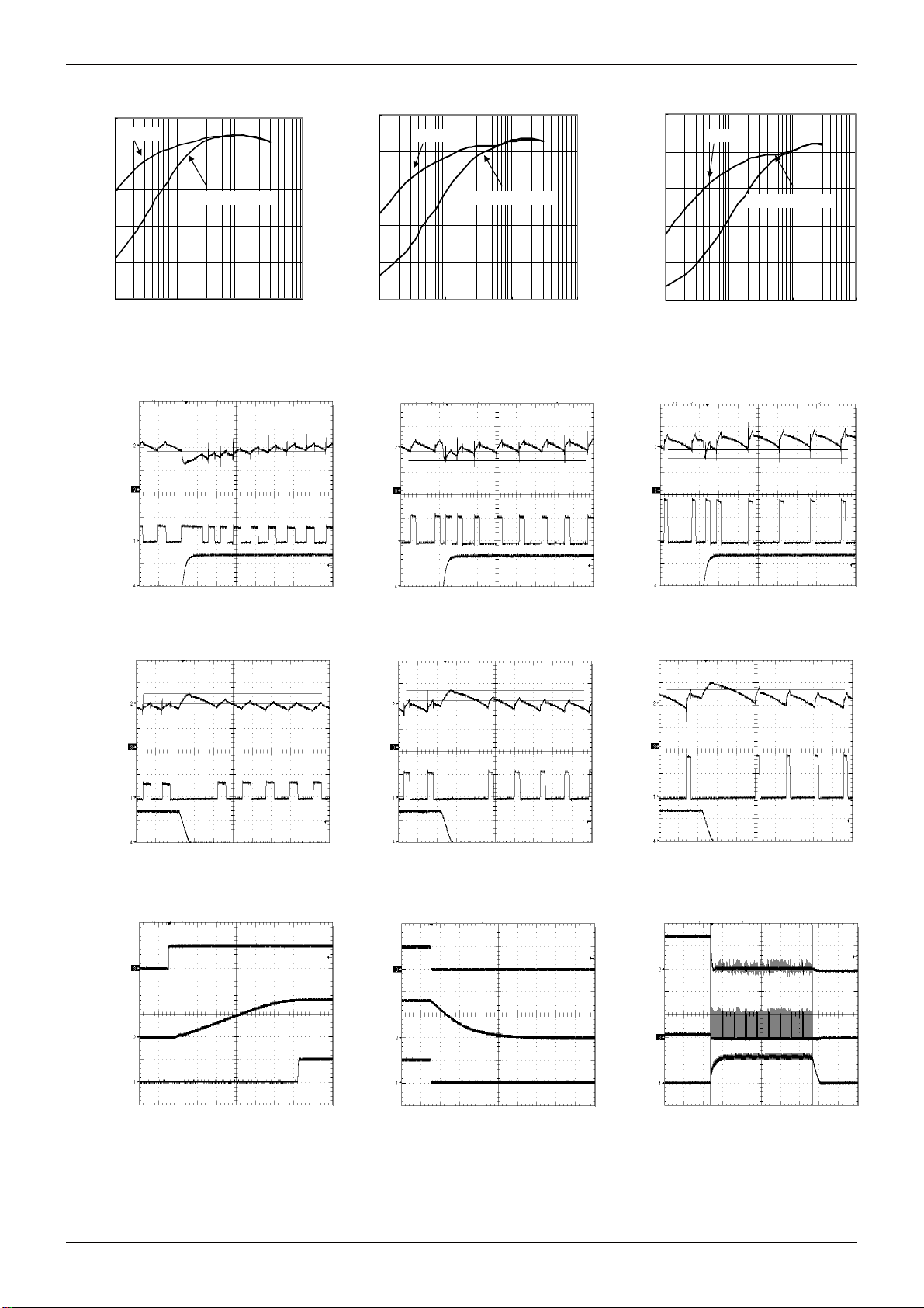
●Reference Data
100
[%]
SLLM
80
60
40
Continuous Mode
20
0
0.01 0.1 1 10
Fig.1 Io-Efficiency
IN=7V,VOUT=2.5V)
(V
Io [A]
(50mV/div)
VOU
2sec/div
SW
(10V/div)
IOUT
(2A/div)
Fig.4 Transient Response
IN=7V, VOUT=2.5V)
(V
(50mV/div)
VOU
2sec/div
SW
(10V/div)
IOUT
(2A/div)
Fig.7 Transient Response
IN=7V, VOUT=2.5V)
(V
200sec/div 2msec/div
EN
VOUT
2[V/div]
PGOOD PGOOD
Fig.10 PGOOD Rising
Waveform
100
SLLM SLLM
80
60
[%]
40
20
0
0. 01 0. 1 1 10
Continuous Mode
Io [A]
Fig.2 Io-Efficiency
(VIN=12V,VOUT=2.5V)
VOU
(50mV/div)
SW
(10V/div)
IOUT
(2A/div)
Fig.5 Transient Response
(VIN=12V, VOUT=2.5V)
VOUT
(50mV/div)
SW
(10V/div)
IOUT
(2A/div)
Fig.8 Transient Response
(V
IN=12V, VOUT=2.5V)
EN
OUT
V
2[V/div]
Fig.11 PGOOD Falling
Waveform
100
80
60
[%]
40
20
0
0.01 0.1 1 10
Continuous Mode
Io [A]
Fig.3 Io-Efficiency
(VIN=19V,VOUT=2.5V)
2sec/div 2sec/div
VOUT
(50mV/div)
SW
(10V/div)
IOUT
(2A/div)
Fig.6 Transient Response
IN=19V, VOUT=2.5V)
(V
2sec/div 2sec/div
VOU
(50mV/div)
SW
(10V/div)
IOUT
(2A/div)
Fig.9 Transient Response
(VIN=19V, VOUT=2.5V)
V
OUT
2[V/div]
SW
5[A/div]
I
L
200sec/div
Fig.12 SCP Timer Latch
Waveform
www.rohm.com
© 2009 ROHM Co., Ltd. All rights reserved.
4/15
2009.04 - Rev.B
Page 5
BD95514MUV
k
A
A
●Reference Data
EN
REG
V
2[V/div]
OUT
V
2[V/div]
SW
Fig.13 EN wake up
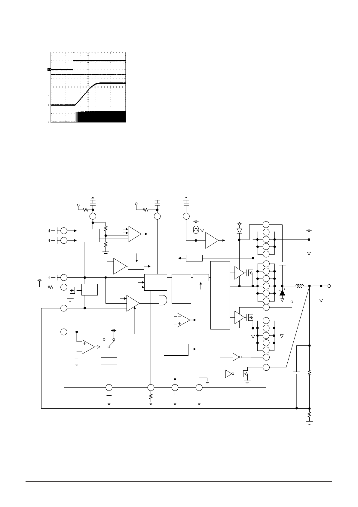
●Block Diagram
REG
V
EN
CTL
REF(0.7V)
PGOOD
FB
EXTV
10
8
17
6
18
CC
14
VREG
Reference
Block
400sec/div
13
VREF×0.85
V
SS×0.85
Power
Good
VCC
V
OUT
5V Reg
15
REG
AVIN
SS
VIN
REG
MODE
UVLO
ILIM
SCP
TSD
V
IN
OVP
Delay
EN
UVLOV
SCP
H3Reg
Controller
Bloc
11
VIN SS
7
ILIM
TM
REF×1.2
FB
Thermal
Protection
MODE
FS V
16
Soft Start
OCP
RSQ
912
MODE
OVP
TSD
MODE
GND MODE
Driver
Circuit
EN/UVLO
SS
Technical Note
DD
V
HG
LG
5
1
2
3
4
26
27
28
29
30
31
21
22
23
24
25
32
20
19
BOOT
V
IN
SW
DD
V
PGND
CE
OUT
V
VREG
VIN(4.5~28V)
OUT
V
www.rohm.com
© 2009 ROHM Co., Ltd. All rights reserved.
5/15
2009.04 - Rev.B
Page 6
BD95514MUV
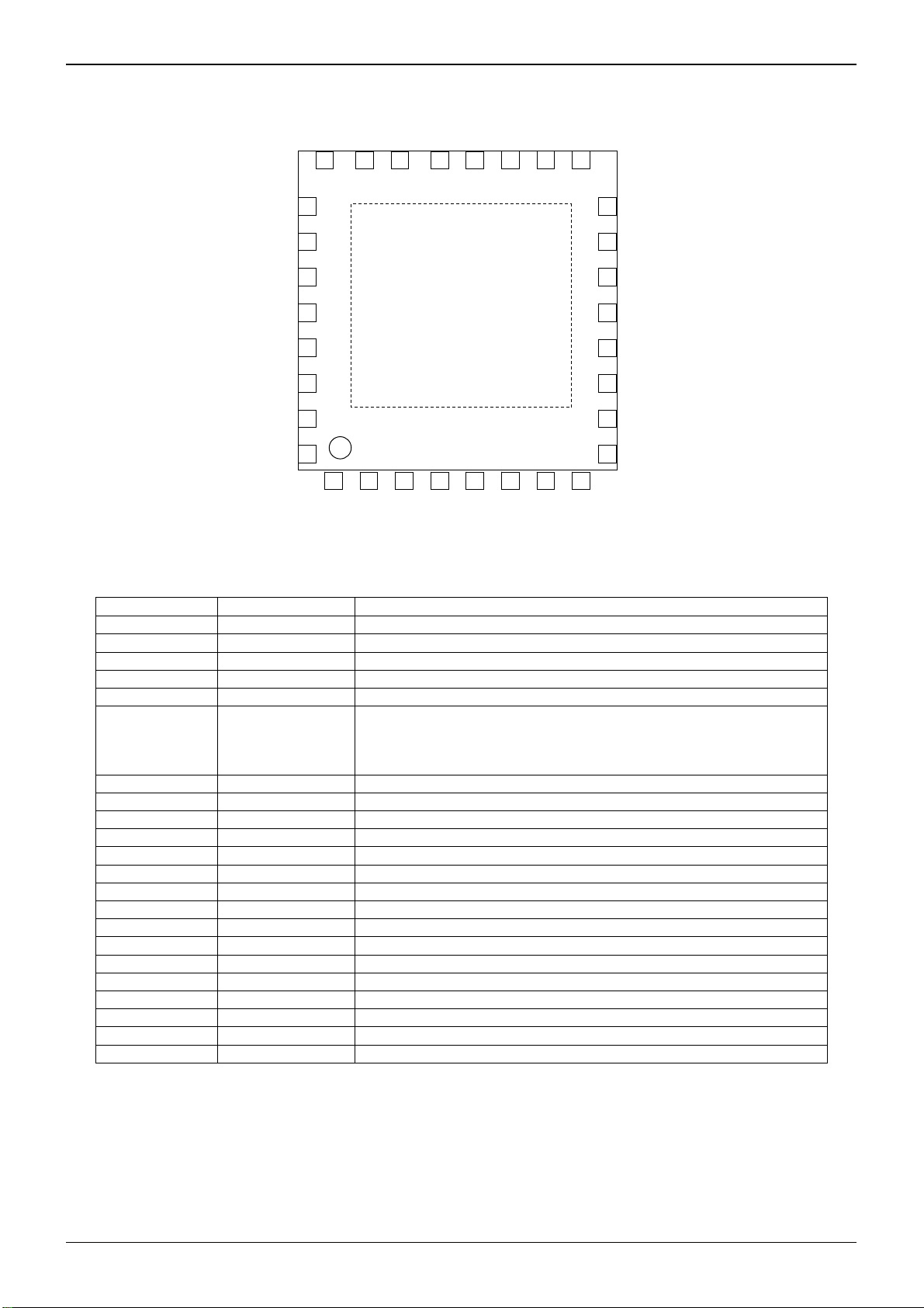
●Pin Configuration
PGND
SW
SW
25
26
27
22 21 20
23 24
22 21 20
23 24
19 18 17
19 18 17
16
15
14
SS
REG
V
EXTVcc
Technical Note
●Pin Function Table
PIN No. PIN Name PIN Function
1-4 VIN Battery voltage input (4.5 ~ 28 V)
5 BOOT HG driver power supply
6 PGOOD Power good output (high when output ±10% of regulation)
7 AVIN Battery voltage sense
8 CTL Linear regulator on/off (high = 5.0V, low = off)
9 MODE
10 EN Enable output (high when VOUT ON)
11 FS Switching frequency adjustment(RFS = 30 k ~ 300 k)
12 GND Sense ground
13 VCC Power supply input
14 EXTVCC External power supply input
15 VREG IC reference voltage (5.0V / 100mA)
16 SS Soft start condenser input
17 REF Output reference voltage (0.7 V)
18 FB Feedback input (0.7 V)
19 VOUT Voltage discharge output
20 CE Reversing HG output
21 VDD Power supply input (5 V)
22-25 PGND Power ground
26-31 SW Output to inductor
32 PGND Power ground
Underside FIN Substrate connection
28
SW
SW
29
SW
30
SW
31
PGND
32
1 2 3 4 5 6
V
IN VIN VIN VIN BOOT PGOOD
*Connect the underside (FIN) to the ground terminal
*Connect the underside (FIN) to the ground terminal
AV
Control mode selection
GND:Continuous Mode
3.0V:QLLM
VCC:SLLM
V
CC
13
GND
12
FS
11
EN
10
MODE
9
7
8
CTL
IN
www.rohm.com
© 2009 ROHM Co., Ltd. All rights reserved.
6/15
2009.04 - Rev.B
Page 7

BD95514MUV
Technical Note
●Pin Descriptions
・VCC
This pin supplies power to the IC’s internal circuitry, excluding the FET driver. The input supply voltage range is 4.5 to 5.5 V.
This pin should be bypassed with either a power capacitor or RC filter.
・EN
Enables or disables the switching regulator. When the voltage on this pin reaches 2.3V or higher, the internal switching
regulator is turned on. At voltages less than 0.8V, the regulator is turned off.
DD
・V
This pin supplies power to the low side of the FET driver, as well as to the bootstrap diode. As the diode draws its peak
current when switching on or off, this pin should be bypassed with a capacitance of approximately 1µF.
REG
・V
Output pin from the 5V linear regulator. This pin also supplies power to the internal driver and control circuitry.
REG standby function is controlled by the CTL pin. The output supplies 5V at 100mA and should be bypassed to ground
V
using a 10 µF capacitor with a rating of X5R or X7R.
・EXTVCC
External power supply input for the linear regulator. When the voltage on the EXTVCC pin exceeds 4.4V, the regulator
uses it in conjunction with other power sources to supply V
REG. Connect the EXTVCC pin to GND when not in use.
・REF
Reference voltage output pin. The reference voltage is set internally by the IC to 0.7V, and the IC works to keep V
approximately equal to V
FB. Variations in voltage levels on this pin affect the output voltage, so the pin should be
bypassed with a 100pF ~ 0.1µF ceramic capacitor.
・SS
Soft start pin. When EN is set high, the capacitor between the internal current source(typ:2.2A) and SS-GND controls
the startup time of the IC. When the voltage on the SS pin is lower than the REF output voltage (0.7V), the output voltage
is held at the same voltage as the SS pin.
IN
・AV
The BD95514MUV controls the duty cycle and output voltage based upon the input voltage at this pin, so voltage
variations or oscillations on this line can cause operation to become unstable. This pin also acts as the voltage input for
the switching block, so insufficient coupling impedance can also cause operation to become unstable. Therefore, this line
should be bypassed with either a power capacitor or RC filter.
・FS
Frequency-adjusting resistance input pin. Attaching a resistance of 30k~300k adjusts the switching frequency from 200
kHz~1MHz (p.11).
・BOOT
This pin serves as the power source for the high side of the FET driver. A bootstrap diode is integrated within the IC.
The maximum voltage on this pin should not exceed +30V vs. GND or +7V vs. SW. When operating the switching
regulator, the operation of the bootstrap circuitry causes the BOOT voltage to swing from (V
IN + VDD) ~ VDD.
・PGOOD
Power good indicator. This open-drain output should be connected via a 100k pull-up resistor.
・MODE
Mode selection pin. When low, the IC functions in forced-continuous mode; at voltages from 0V ~ 3V, QLLM mode;
when high, SLLM mode.
・CTL
Linear regulator control pin. When voltage is 2.3V or higher, a logic HIGH is recognized and the internal regulator
REG = 5 V) is switched on. At voltages of 0.8V or lower, a logic LOW is recognized and the regulator is switched off.
(V
However, even if EN is logic HIGH, the switching regulator will not operate if CTL is logic LOW.
・FB
Output voltage feedback input. V
FB is held at 0.7V by the IC.
・SW
Output from the switching regulator to the inductor. This output swings from V
IN ~ GND. The trace from the output to
the inductor should be as short and wide as possible.
OUT
・V
Voltage output discharge pin. When EN is off, this output is pulled low.
IN
・V
Power supply input. The IC can accept any input from 4.5V to 28V. This pin should be bypassed directly to ground by a
power capacitor.
・PGND
Power ground terminal.
REF
www.rohm.com
© 2009 ROHM Co., Ltd. All rights reserved.
7/15
2009.04 - Rev.B
Page 8

BD95514MUV
r
A
r
f
A
Technical Note
●Operation
The BD95514MUV is a switching regulator incorporating ROHM’s proprietary H3RegTM CONTROLLA control system.
When V
OUT drops suddenly due to changes in load, the system quickly restores the output voltage by extending the ton time
interval. This improves the regulator’s transient response. When light-load mode is activated, the IC employs the Simple
Light Load Mode (SLLM) controller, further improving system efficiency.
3
RegTM Control
H
(Normal Operation)
VFB
VREF
HG
LG
When VFB falls below the reference voltage (0.7V), the
3
H
RegTM CONTROLLA is activated;
t
ON
VREF
IN
V
×
1
f
[sec]・・・(1)
High gate output is determined by the above formula.
(Rapid Changes in Load)
VFB
VREF
Io
ON+α
t
When V
the voltage remains below V
preprogrammed t
system quickly restores V
thereby improving transient response.
drops due to a sudden change in load and
OUT
time interval has elapsed, the
ON
by extending the tON time,
OUT
after the
REF
HG
LG
Light Load Control
(SLLM Mode)
VREF
HG
LG
VFB
SLLM mode is enabled by setting the MODE pin to logic
high. When the low gate is off and the current through
the inductor is 0 (current flowing from V
to SW), the
OUT
SLLM function is activated, disabling high gate output.
falls below V
If V
FB
again, the high gate is switched
REF
back on, lowering the switching frequency of the regulato
and yielding higher efficiency when powering light loads.
0
(QLLM Mode)
VREF
VFB
HG
LG
0
QLLM mode is enabled by setting the MODE pin to HiZ o
middle voltage. When the lower gate is off and the
current through the inductor is 0 (current flowing from
VOUT to SW), QLLM mode is activated, disabling high
gate output.
If VFB falls below VREF within a programmed time
interval (typ. 40µs), the high gate is switched on, but i
VFB does not fall below VREF, the lower gate is forced
on, dropping VFB and switching the high gate back on.
The minimum switching frequency is set to 25 kHz (T=40
µS), which keeps the regulator’s frequency from entering
the audible spectrum but yields less efficient results than
SLLM mode.
www.rohm.com
© 2009 ROHM Co., Ltd. All rights reserved.
8/15
2009.04 - Rev.B
Page 9

BD95514MUV
f
T
●Timing Chart
・Soft Start Function
EN
tSS
SS
OU
V
IIN
・Timer Latch-type Short Circuit Protection
VREF×0.70
VOUT
1ms
SCP
EN/UVLO
・Output Over-Voltage Protection
REF×1.2
VOUT
V
HG
LG
Switching
Technical Note
The soft start function is enabled when the EN pin is set
high. Current control circuitry takes effect at startup,
yielding a moderate “ramping start” in output voltage.
Soft start timing and incoming current are given by
equation (2) and (3) below:
Soft start period:
REF×Css
V
=
t
SS
2.2A(typ)
Rush current:
OUT
IN(ON)=
I
Co×V
tss
(Css: soft start capacitor;
Co: All capacitors connected with VOUT)
When output voltage falls to V
output short circuit protection engages, turning the IC of
after a set period of time to prevent internal damage.
When EN is switched back on or when UVLO is cleared,
output continues. The time period before shutting off is
set internally at 1 ms.
When output reaches or exceeds V
over-voltage protection is engaged, turning the low-side
FET completely on to reduce the output (low gate on, high
gate off). When the output falls, it returns to standard
mode.
[sec]
・・・(2)
・・・(3)
[A]
REF x 0.70 or less, the
x 1.2, the output
REF
www.rohm.com
© 2009 ROHM Co., Ltd. All rights reserved.
9/15
2009.04 - Rev.B
Page 10

BD95514MUV
A
r
[A]
[H]
t
(
)
[A]
Technical Note
●External Component Selection
1. Inductor (L) Selection
VIN
ΔIL
IL
OUT
V
L
Co
The inductor’s value directly influences the output ripple current.
s formula (4) indicates below, the greater the inductance o
switching frequency, the lower the ripple current:
(VIN-VOUT)×VOUT
ΔIL=
The proper output ripple current setting is about 30% of maximum output
current.
L×V
IN×f
・・・(4)
ΔIL=0.3×IOUTmax. [A]・・・(5)
(V
IN-VOUT)×VOUT
L=
(ΔI
L: output ripple current, f: switching frequency)
ΔI
L×VIN×f
・・・(6)
Output ripple current
※ Passing a current larger than the inductor’s rated current will cause magnetic saturation in the inductor and decrease
system efficiency. In selecting the inductor, be sure to allow enough margin to assure that peak current does not exceed
the inductor’s rated current value.
※ To minimize possible inductor damage and maximize efficiency, choose an inductor with a low DCR and ACR resistance.
V
OUT
)
O
When determining the proper output capacitor, be sure to factor in the equivalent
series resistance (ESR) and equivalent series inductance (ESL) required to se
the output ripple voltage at 20 mV or more.
When selecting the limit of the inductor, be sure to allow enough margin for the
output voltage. Output ripple voltage is determined by formula (7) below:
ΔV
OUT=ΔIL×ESR+ESL×ΔIL / TON・・・(7)
L: Ouput ripple current, ESR: equivalent series resistance,
(ΔI
ESL: equivalent series inductance)
2. Output Capacitor Selection (C
VIN
L
Output Capacitor
ESR
ESL
Co
Give special consideration to the conditions of formula (7) for output capacitance. Also, keep in mind that the output rise
time must be established within the soft start timeframe.
Co≦
tss×(I
V
limit-IOUT)
OUT
・・・(8)
tss: Soft start timeframe (see p. 10, equation (2))
I
: Maximum output current
limit
Choosing a capacitance that is too large can cause startup malfunctions, or in some cases, may engage the short circuit
protection.
3. Input Capacitor Selection (C
VIN
CIN
L
Co
)
IN
In order to prevent extreme over-current conditions, the input capacitor must
have a low enough ESR to fully support a large ripple in the output. The
formula for RMS ripple current (I
V
OUT
IRMS=IOUT×
√
IN
V
VIN-VOUT
VIN
) is given by equation (9) below:
RMS
・・・(9)
IOUT
When VIN=2×VOUT, IRMS=
2
Input Capacitor
A low-ESR capacitor is recommended to reduce ESR loss and maximize efficiency.
www.rohm.com
© 2009 ROHM Co., Ltd. All rights reserved.
10/15
2009.04 - Rev.B
Page 11

BD95514MUV
A
Technical Note
4. Frequency Adjustment
500
450
400
350
300
250
200
Frequency [kHz]
150
100
50
0
50 100 150 200 250 300
From top:VIN=
RFS[k]
5V
7V
12V
19V
25V
The resistance connected to the FS terminal adjusts the
on-time (t
the left. When t
) during normal operation as illustrated to
ON
, input voltage and VREF voltage are
ON
known, the switching frequency can be determined by
the following formula:
F=
・・・(10)
V
REF
IN×tON
V
However, real-life considerations (such as external
MOSFET gate capacitance and switching time) must be
factored in as they affect the overall switching rise and
fall time. This leads to an increase in t
ON
total frequency slightly.
dditionally, when output current lingers around 0A in
continuous mode, this “dead time” also has an effect
upon t
, further lowering the switching frequency.
ON
Confirm the switching frequency by measuring the
current through the coil (at the point where current does
not flow backwards) during normal operation.
The BD95514MUV operates by feeding the output voltage back through a resistive voltage divider. The output voltage is
set by the following equation (see schematic below):
Output Voltage = ×
R1+R2
R2
VREF (0.7V) + ×ΔIL×ESR・・・(11)
1
2
The switching frequency is also amplified by the same resistive voltage divider network:
sw = ×(frequency set by RFS) [Hz]・・・(12)
f
R1+R2
R2
REF(0.7V)
CONTROLLA
FB
VIN
H3RegTM
RQ
S
SLLM
SLLM
TM
Driver
Circuit
, lowering the
VIN
Output Voltage
ESR
R1
R2
www.rohm.com
© 2009 ROHM Co., Ltd. All rights reserved.
11/1 5
2009.04 - Rev.B
Page 12

BD95514MUV
A
W
Technical Note
●Evaluation Board Circuit (Frequency=300kHz Continuous Mode/QLLM/SLLM Example Circuit)
SW
L1
VOUT
GND_VIN
VIN
VIN
D1
C14
PGOOD
VDD
R9
R4 R22
VDD
C7
SW3
VDD
SW1
C10
C11
C12
C8
C9
D
R17 SW2
VIN
VIN
VIN
VIN
BOOT
PGOOD
VIN
CTL REF
CTL
MODE
EN
SWSWSWSWSWS
PGND
MODE
EN
FS
GND
R6
VCC
GND
VCC
PGND
PGND
PGND
PGND
VDD
CE
VOUT
FB
EXTVCC
VREG
SS
C5C4R2C2C1
R1
VREG
C6 C19
R5
SS
R18
R7 C13
R8
VDD
GND PGND
VCC EXTVCC
●Evaluation Board Parts List
Designation Rating PART No. Company Designation Rating PART No. Company
R1 10 MCR03 ROHM C03 1F ceramic capacitor -
R2 0 MCR03 ROHM C04 1F ceramic capacitor -
R3 - - - C05 3300pF ceramic capacitor R4 10 MCR03 ROHM C06 0.1F ceramic capacitor R5 10K MCR03 ROHM C07 0.1F ceramic capacitor R6 270K MCR03 ROHM C08 - - R7 10k MCR03 ROHM C09 - - R8 3.07k MCR03 ROHM C10 - - R9 100K MCR03 ROHM C11 22F ceramic capacitor -
R10 - - - C12 0.1F ceramic capacitor R11 - - - C13 1000pF ceramic capacitor R12 - - - C14 220F 4TPE220MF SANYO
R13 - - - C15 - - R14 - - - C16 - - R15 0 MCR03 ROHM C17 - - R16 0 MCR03 ROHM C18 - - R17 0 MCR03 ROHM C19 470pF ceramic capacitor R18 0 MCR03 ROHM D1 - RSX501L-20 ROHM
R22 510k MCR03 ROHM D - TDZ5.1 ROHM
C01 1F ceramic capacitor - L1 3.2H CDEP105-3R2MC-50 Sumida
C02 - - - U1 - BD95514MUV ROHM
VOUT
GND_VOUT
GND_VDD
REF
VDD
www.rohm.com
© 2009 ROHM Co., Ltd. All rights reserved.
12/15
2009.04 - Rev.B
Page 13

BD95514MUV
●Operation Notes
(1) Absolute maximum ratings
Exceeding the absolute maximum ratings (such as supply voltage, temperature range, etc.) may result in damage to the
device. In such cases, it may be impossible to identify problems such as open circuits or short circuits. If any
operational values are expected to exceed the maximum ratings for the device, consider adding protective circuitry
(such as fuses) to eliminate the risk of damaging the IC.
(2) Power supply polarity
Connecting the power supply in reverse polarity can cause damage to the IC. Take precautions when connecting the
power supply lines. An external power diode can be added.
(3) Power supply lines
The PCB layout pattern should be designed to provide the IC with low-impedance GND and supply lines. To minimize
noise on the supply and GND lines, ground and power supply lines of analog and digital blocks should be separated.
For all power lines supplying ICs, connect a bypass capacitor between the power supply and the GND terminal. If
using electrolytic capacitors, keep in mind that their capacitance is reduced at lower temperatures.
(4) GND voltage
The potential of the GND pin must be the minimum potential in the system in all operating conditions.
(5) Thermal design
Use thermal design techniques that allow for a sufficient margin for power dissipation in actual operating conditions.
(6) Inter-pin shorts and mounting errors
Use caution when positioning he IC for mounting on PCBs. The IC may be damaged if there are any connection errors
or if pins are shorted together.
(7) Operation in strong electromagnetic fields
Exercise caution when using the IC in the presence of strong electromagnetic fields as doing so may cause the IC to
malfunction.
(8) ASO
When using the IC, set the output transistor so that it does not exceed either absolute maximum ratings or ASO.
(9) Thermal shutdown circuit
The IC incorporates a built-in thermal shutdown circuit (TSD circuit), which is designed to shut down the IC only to
prevent thermal overloading. It is not designed to protect the IC or guarantee its operation. Do not continue to use
the IC if this circuit is activated, or in environments in which activation of this circuitry can be assumed.
(10) Testing on application boards
When testing the IC with application boards, connecting capacitors directly to low-impedance terminals can subject the
IC to stress. Always discharge capacitors completely after each process or step. The IC’s power supply should be
turned off completely before connecting it to or removing it from a jig or fixture during the evaluation process. To
prevent damage from static discharge, ground the IC during assembly and use similar precautions during transport and
storage.
TSD ON Temp. [°C] (typ.) Hysteresis Temp. [°C] (typ.)
BD95514MUV 175 15
Technical Note
www.rohm.com
© 2009 ROHM Co., Ltd. All rights reserved.
13/15
2009.04 - Rev.B
Page 14

BD95514MUV
(11) Regarding IC input pins
This monolithic IC contains P+ isolation and P substrate layers between adjacent elements in order to keep them
isolated. PN junctions are formed at the intersection of these P layers with the N layers of other elements, creating
parasitic diodes and/or transistors. For example (refer to the figure below):
・When GND > Pin A and GND > Pin B, the PN junction operates as a parasitic diode
・When GND > Pin B, the PN junction operates as a parasitic transistor
Parasitic diodes occur inevitably in the structure of the IC, and the operation of these parasitic diodes can result in
mutual interference among circuits, operational faults, or physical damage. Accordingly, conditions that cause these
diodes to operate, such as applying a voltage lower than the GND voltage to an input pin (and thus to the P substrate)
should be avoided.
Resistance
Pin A
N
P+ P
P
Parasitic Element
GND
(12) (12) Ground wiring traces
When using both small-signal and large-current GND traces, the two ground traces should be routed separately but
connected to a single ground potential within the application in order to avoid variations in the small-signal ground
caused by large currents. Also ensure that the GND traces of external components do not cause variations on GND
voltage.
●Power Dissipation
5.5
5.0
④4.56W
4.5
4.0
3.5
3.0
2.5
③2.06W
Power Dissipation Pd [W]
2.0
1.5
②0.88W
1.0
①0.38W
0.5
0
0 20 40 60 80 100 120
Ambient Temperature Ta [°C]
Pin A
+
N N
P Substrate
VQFN032V5050
Pin B
N
P+
Parasitic Element
Parasitic Elements
Example of IC Structure
140
Technical Note
Transistor (NPN)
B
C
B
E
N
P
P+
N
P 基板
GND
GND
① IC Only
θ
= 328.9 °C/W
j-a
② IC mounted on 1-layer board (with 20.2 mm
= 142.0 °C/W
θ
j-a
③ IC mounted on 4-layer board (with 20.2 mm
5502 mm
2
pad on layers 2,3)
θ
= 60.7 °C/W
j-a
④ IC mounted on 4-layer board (with 5505mm
端子 B
B C
E
GND
Other Adjacent Elements
Parasitic Elements
2
copper thermal pad)
2
pad on top layer,
2
pad on all layers)
www.rohm.com
© 2009 ROHM Co., Ltd. All rights reserved.
14/15
2009.04 - Rev.B
Page 15

BD95514MUV
Technical Note
●Ordering part number
B D 9 5 5 1 4 M U V - E 2
Part No. Part No.
VQFN032V5050
5.0± 0.1
1.0MAX
0.08 S
0.75
C0.2
0.4± 0.1
32
25
5.0± 0.1
3.4± 0.1
24
0.5
17
1PIN MARK
+0.03
0.02
81
9
16
+0.05
0.25
-
0.04
0.02
-
3.4± 0.1
S
(0.22)
(Unit : mm)
Package
MUV : VQFN032V5050
<Tape and Reel information>
Embossed carrier tapeTape
Quantity
Direction
of feed
2500pcs
E2
The direction is the 1pin of product is at the upper left when you hold
()
reel on the left hand and you pull out the tape on the right hand
Reel
1pin
Packaging and forming specification
E2: Embossed tape and reel
Direction of feed
Order quantity needs to be multiple of the minimum quantity.
∗
www.rohm.com
© 2009 ROHM Co., Ltd. All rights reserved.
15/15
2009.04 - Rev.B
Page 16

Notes
No copying or reproduction of this document, in part or in whole, is permitted without the
consent of ROHM Co.,Ltd.
The content specied herein is subject to change for improvement without notice.
The content specied herein is for the purpose of introducing ROHM's products (hereinafter
"Products"). If you wish to use any such Product, please be sure to refer to the specications,
which can be obtained from ROHM upon request.
Examples of application circuits, circuit constants and any other information contained herein
illustrate the standard usage and operations of the Products. The peripheral conditions must
be taken into account when designing circuits for mass production.
Great care was taken in ensuring the accuracy of the information specied in this document.
However, should you incur any damage arising from any inaccuracy or misprint of such
information, ROHM shall bear no responsibility for such damage.
The technical information specied herein is intended only to show the typical functions of and
examples of application circuits for the Products. ROHM does not grant you, explicitly or
implicitly, any license to use or exercise intellectual property or other rights held by ROHM and
other par ties. ROHM shall bear no responsibility whatsoever for any dispute arising from the
use of such technical information.
Notice
The Products specied in this document are intended to be used with general-use electronic
equipment or devices (such as audio visual equipment, ofce-automation equipment, communication devices, electronic appliances and amusement devices).
The Products specied in this document are not designed to be radiation tolerant.
While ROHM always makes efforts to enhance the quality and reliability of its Products, a
Product may fail or malfunction for a variety of reasons.
Please be sure to implement in your equipment using the Products safety measures to guard
against the possibility of physical injury, re or any other damage caused in the event of the
failure of any Product, such as derating, redundancy, re control and fail-safe designs. ROHM
shall bear no responsibility whatsoever for your use of any Product outside of the prescribed
scope or not in accordance with the instruction manual.
The Products are not designed or manufactured to be used with any equipment, device or
system which requires an extremely high level of reliability the failure or malfunction of which
may result in a direct threat to human life or create a risk of human injury (such as a medical
instrument, transportation equipment, aerospace machinery, nuclear-reactor controller,
fuel-controller or other safety device). ROHM shall bear no responsibility in any way for use of
any of the Products for the above special purposes. If a Product is intended to be used for any
such special purpose, please contact a ROHM sales representative before purchasing.
If you intend to export or ship overseas any Product or technology specied herein that may
be controlled under the Foreign Exchange and the Foreign Trade Law, you will be required to
obtain a license or permit under the Law.
www.rohm.com
© 2009 ROHM Co., Ltd. All rights reserved.
Thank you for your accessing to ROHM product informations.
More detail product informations and catalogs are available, please contact us.
ROHM Customer Support System
http://www.rohm.com/contact/
R0039
A
 Loading...