

Page 1

High Performance Regulators for PCs
Switching Regulator
with MOSFET for DDR-SDRAM Cores
BD95500MUV
●Description
BD95500MUV is a switching regulator with high output current (up to 6A) which can achieve low output voltage
(0.7V to 5.0V) from a wide input voltage range (3V to 20V). High efficiency for the switching regulator can be realized by
utilizing an internal N-MOSFET power transistor. A new technology called H
realize ultra high transient response against load change. SLLM (Simple Light Load Mode) technology is also integrated to
improve efficiency in light load mode, providing high efficiency over a wide load range. For protection and ease of use, the
soft start function, variable frequency function, short circuit protection function with timer latch, over voltage protection
function, and power good function are all built in. This switching regulator is specially designed for sets of various kinds.
●Features
1) Integrated low ON resistance N-MOSFET (TYP. 50mΩ)
2) H
3) Adjustable Simple Light Load Mode (SLLM), and forced continuous mode
4) Thermal Shut Down (TSD), Under Voltage LockOut (UVLO), Adjustable Over Current Protection (OCP),
Over Voltage Protection (OVP), Short Circuit Protection(SCP) built-in
5) Soft start function to minimize rush current during startup
6) Adjustable switching frequency (f=200KHz~1000KHz)
7) Built-in output discharge function
8) VQFN040V6060 Package
9) Tracking Function
10) Integrated boot strap diode
11) Power Good function
●Applications
Mobile PC, Desktop PC, LCD-TV, Digital Components, etc
3
RegTM DC/DC converter controller
3
RegTM is a Rohm proprietary control method to
No.10030ECT21
www.rohm.com
© 2010 ROHM Co., Ltd. All rights reserved.
1/20
2010.05 - Rev.C
Page 2
BD95500MUV
Technical Note
●Maximum Absolute Ratings (Ta=25℃)
Parameter Symbol Ratings Unit
Input Voltage 1 VCC 7 *1 V
Input Voltage 2 VDD 7 *1 V
Input Voltage 3 VIN 24 *1 V
BOOT Voltage BOOT 30 V
BOOT-SW Voltage BOOT-SW 7 V
LG Voltage LG VDD V
REF Voltage REF VCC V
Output Voltage VOUT/Is+/Is- VCC V
ILIM/SS/FS/MODE Voltage ILIM/SS/FS/MODE VCC V
VREG Voltage VREG VCC V
EN Input Voltage EN 7 V
Output Current (Average) Isw 6 A
Power Dissipation 1 Pd1 0.54 *2 W
Power Dissipation 2 Pd2 1.00 *3 W
Power Dissipation 3 Pd3 3.77 *4 W
Power Dissipation 4 Pd4 4.66 *5 W
Operating Temperature Range Topr -10~+100 ℃
Storage Temperature Range Tstg -55~+150 ℃
Junction Temperature Tjmax +150 ℃
*1 Not to exceed Pd, ASO, and Tjmax=150℃.
*2 Reduced by 4.3mW for each increase in Ta of 1℃ over 25℃ (when don’t mounted on a heat radiation board )
*3 Reduced by 8.0mW for increase in Ta of 1℃ over 25℃. (when mounted on a board 70.0mm×70mm×1.6mm Glass-epoxy PCB which has 1 layer.
(Copper foil area : 0mm
*4 Reduced by 30.1mW for increase in Ta of 1℃ over 25℃. (when mounted on a board 70.0mm×70mm×1.6mm Glass-epoxy PCB which has 4 layers.
st
(1
and 4th copper foil area : 20.2mm2, 2nd and 3rd copper foil area : 5505mm2))
*5 Reduced by 37.3mW for increase in Ta of 1℃ over 25℃. (when mounted on a board 70.0mm×70mm×1.6mm Glass-epoxy PCB which has 4 layers.
(All copper foil area : 5505mm
2
))
2
))
●Operating Conditions (Ta=25℃)
Parameter
Symbol
MIN MAX
Ratings
Unit
Input Voltage 1 VCC 4.5 5.5 V
Input Voltage 2 VDD 4.5 5.5 V
Input Voltage 3 VIN 3.0 20 V
BOOT Voltage BOOT 4.5 25 V
SW Voltage SW -0.7 20 V
BOOT-SW Voltage BOOT-SW 4.5 5.5 V
MODE Input Voltage MODE 0 5.5 V
EN Input Voltage EN 0 5.5 V
Output Adjustable Voltage REF 0.7 2.0 V
Is Input Voltage Is+/Is- 0.7 2.7 V
MIN ON Time Tonmin - 200 nsec
*This product should not be used in a radioactive environment.
www.rohm.com
© 2010 ROHM Co., Ltd. All rights reserved.
2/20
2010.05 - Rev.C
Page 3
BD95500MUV
●Electrical characteristics
(Unless otherwise noted, Ta=25℃, VCC=5V, VDD=5V, EN / MODE=5V, VIN=12V, REF=1.8V, RFS=68kΩ)
Parameter Symbol
[Whole Device]
VCC Bias Current Icc - 1200 2000 μA
VIN Bias Current Iin - 100 200 μA
VCC Standby Current Iccstb - 0 10 μA EN=0V
VIN Standby Current Iinstb - 0 10 μA EN=0V
EN Low Voltage Enlow GND - 0.8 V
EN High Voltage Enhigh 2.3 - 5.5 V
EN Bias Current Ien - 7 10 μA
VREG Voltage Vreg 2.475 2.500 2.525 V
[Under Voltage Locked Out ]
VCC Threshold Voltage Vcc_UVLO 4.1 4.3 4.5 V VCC:Sweep up
VCC Hysteresis Voltage dVcc_UVLO 100 160 220 mV VCC:Sweep down
VIN Threshold Voltage Vin_UVLO 2.4 2.6 2.8 V VIN:Sweep up
VIN Hysteresis dVin_UVLO 100 160 220 mV VIN:Sweep down
VREG Threshold Voltage Vreg_UVLO 2.0 2.2 2.4 V VREG:Sweep up
VREG Hysteresis Voltage dVreg_UVLO 100 160 220 mV VREG:Sweep down
[H3REGTM Control Block]
ON Time Ton 400 500 600 nsec
MAX ON Time Tonmax - 3 6.0 μsec
MIN OFF Time Toffmin - 450 550 nsec
[FET Block]
High Side ON Resistance HGhon - 50 80 mΩ
Low Side ON Resistance HGlon - 50 80 mΩ
[SCP Block]
SCP Start up Voltage Vscp REF×0.60 REF×0.70 REF×0.80 V
Delay Time Tscp - 1.0 2.0 ms
[OVP Block]
OVP Detect Voltage Vovp REF×1.16 REF×1.2 REF×1.24 V
[Soft Start Block]
Charge Current Iss 2 4 6 μA
Discharge Current Idis 0.5 1.0 2.0 μA
Standby Voltage Vss_stb - - 50 mV
[Over Current Protection Block]
Current Limit Threshold 1 Ilim1 40 50 60 mV
Current Limit Threshold2 Ilim2 160 200 240 mV ILIM=2.0V
[Vout Setting]
VOUT Offset Voltage 1 Voutoff1 REF-10m REF REF+10m V Ta=-10℃ to 100℃
VOUT Bias Current Ivout -100 0 100 nA
REF Bias Current Iref -100 0 100 nA
Is+ Input Current IIs+ -1 0 1 μA Is+=1.8V
Is- Input Current IIs- -1 0 1 μA Is-=1.8V
[MODE Block]
SLLM Threshold VthSLLM VCC-0.5 - VCC V
Forced Continuous Mode VthCONT GND - 0.5 V
Input Impedance RMODE - 400 - kΩ
[Power Good Block]
VOUT Power Good Low Voltage VoutPL REF×0.85 REF×0.90 REF×0.95 V
VOUT Power Good High Voltage VoutPH REF×1.05 REF×1.10 REF×1.15 V
Min. Typ. Max.
Limit
Unit Condition
Technical Note
Ireg=0 to 500uA,
Ta =- 10 ℃ to 100℃*
ILIM=0.5V ,
Ta =- 10 ℃ to 100℃
www.rohm.com
© 2010 ROHM Co., Ltd. All rights reserved.
3/20
2010.05 - Rev.C
Page 4
]
]
]
]
]
p
p
BD95500MUV
●Reference Data
2.500
2.498
2.496
2.494
VREG[V
2.492
2.490
-101030 50 7090
Ta(℃)
2.20
2.15
2.10
2.05
VREG[V
2.00
1.95
Sweep down
1.90
-101030507090
Ta(℃)
Fig.4 Ta vs UVLO (VREG)
3
2
1
0
-1
VOUT-REF [mV
-2
-3
-101030507090
Fig.7 Ta vs VOUT Offset
Ta
(℃)
100
80
SLLM
60
[%]
η
40
20
0
0.001 0.01 0.1 1 10
Fig.10 Io vs Efficiency
(V
Forced
Continuous
Io(mA)
IN=7V, VOUT=1.5V)
Sweep up
4.30
4.25
4.20
4.15
VCC[V]
4.10
4.05
4.00
-101030507090
Sweep u
Sweep down
Ta(℃)
Fig.2 Ta vs UVLO (VCC)
2.20
2.15
2.10
2.05
VREG[V
2.00
1.95
1.90
-101030 50 7090
Sweep up
Sweep down
Ta(℃)
Fig.5 Ta vs EN Threshold
54
52
50
Is [mV
⊿
48
46
-101030507090
ILIM=0.5V
Ta (℃)
Fig.8 Ta vs Current Limit
Threshold
100
80
60
[%]
η
40
20
0
0.001 0.01 0.1 1 10
SLLM
Forced
Continuous
Io(mA)
Fig.11 Io vs Efficiency
(VIN=12V, VOUT=1.5V)
Technical Note
2.70
2.65
2.60
2.55
VIN[V]
2.50
2.45
2.40
-101030507090
Fig.3 Ta vs UVLO (VIN) Fig.1 Ta vs VREG
2.8
2.4
2.0
1.6
1.2
VREG(V)
0.8
0.4
0.0
01.534.56
Fig.6 Vcc vs VREG
400
360
320
280
frequency[kHz]
240
200
0 5 10 15 20 25
Fig.9 VIN vs f
100
80
60
[%]
η
40
20
0
0.001 0.01 0.1 1 10
SLLM
Fig.12 Io vs Efficiency
(V
IN=19V, VOUT=1.5V)
Ta(℃)
Vcc(V)
Io=0A
VIN( V)
Io(mA)
Sweep u
Sweep down
Middle: 25℃
Right: -10℃
Io=2A
Forced
Continuous
Left: 100℃
www.rohm.com
© 2010 ROHM Co., Ltd. All rights reserved.
4/20
2010.05 - Rev.C
Page 5

BD95500MUV
●Reference Data
VOUT
HG/LG
IOUT
Fig.13 Transient Response
IN=7V)
(V
VOUT
HG/LG
IOUT
Fig.16 Transient Response
(VIN=7V)
VOUT
IL
HG/LG
Fig.19 SLLM Mode
OUT=0A)
(I
IL
HG/LG/SW
Fig.22 Continuous Mode
(Io=0A)
IL
HG/LG/SW
VOUT
HG/LG
IOUT
Fig.14 Transient Response
(VIN=12V)
VOUT
HG/LG
IOUT
Fig.17 Transient Response
(VIN=12V)
VOUT
IL
HG/LG
Fig.20 SLLM Mode
OUT=0.4A)
(I
Fig.23 Continuous Mode
(Io=4A)
IL
HG/LG/SW
Technical Note
VOUT
HG/LG
IOUT
Fig.15 Transient Response
(VIN=19V)
VOUT
HG/LG
IOUT
Fig.18 Transient Response
(V
IN=19V)
VOUT
IL
HG/LG
Fig.21 SLLM Mode
OUT=1A)
(I
Fig.24 OCP Status
(Io=5A)
www.rohm.com
© 2010 ROHM Co., Ltd. All rights reserved.
5/20
2010.05 - Rev.C
Page 6
V
BD95500MUV
●Reference Data
VIN
HG/LG
VOUT
Fig.25 V
IN change
(5→19V)
1.52
1.51
1.50
Output Voltage [
1.49
Continuous
SLLM
1.48
0.001 0.01 0. 1 1 10
Iout [A]
Fig.28 IOUT vs VOUT
●Block Diagram
EN
VDD
Vcc
5
Reference
39
Block
Vcc
PGOOD
V
REF
REF×0.85
SS×0.85
V
OUT
10
1
OUT
11
Thermal
Protection
Power
Good
EN/UVLO
TSD
6
VIN
ILIM
SCP
TSD
UVLO
VIN
SCP
8
VREG
Delay
SS
UVLO
GND F S
VIN
HG/LG
VOUT
37
H3RegTM
Controller
Block
Fig.26 V
IN change
(19→5V)
500
400
Continuous
300
Continuous
200
Frequency [kHz
100
0
0.001 0.01 0.1 1 10
SLLM
Iout [A]
Fig.29 IOUT vs f
SSVREGVINS
ILIM
ILIM
×
Current
Limit
0.1
9
OVP
SLLM/
MODE
13
2.5VReg
40
MODE N.C.
7
2.5V
REF×1.2
OUT
V
R Q
S
42
SLLM
Soft Start
Is+
Technical Note
EN
SS
OUT
V
PGOOD
Fig.27 EN wake up
60
50
40
]
℃
30
Tc [
Δ
20
10
0
0123456
Io [A]
Fig.30 IOUT vs ΔTc
VDD
BOOT
SS
Driver
Circuit
12
Is-
38
31
VIN
|
36
22
SW
|
29
14
VDD
15
PGND
|
21
30
PGND
3
CE
C IN
3.3V
~
20V
V OUT
C
OUT
5V
www.rohm.com
© 2010 ROHM Co., Ltd. All rights reserved.
6/20
2010.05 - Rev.C
Page 7
BD95500MUV
Technical Note
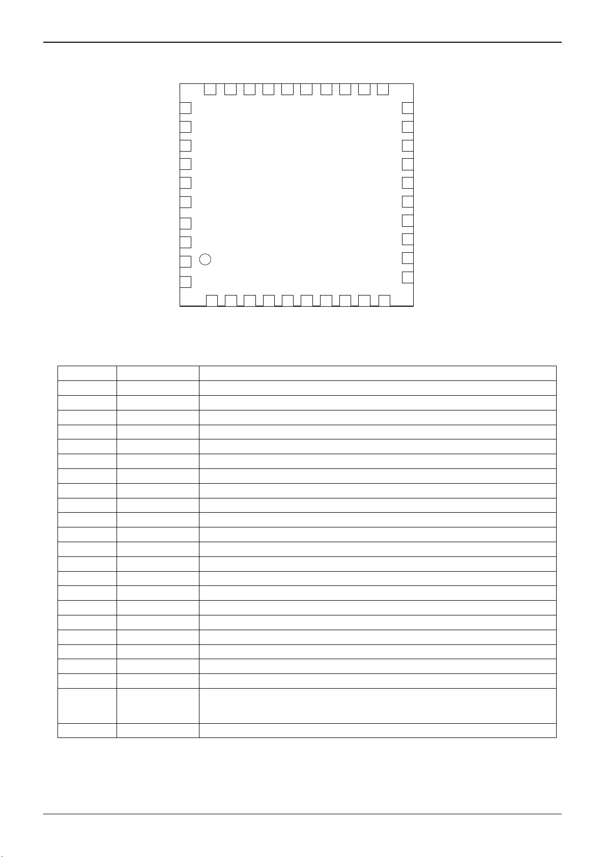
●Pin Configuration
VIN
31
29 28 27 26 25 30
24 23 22
VIN
VIN
VIN
VIN
VIN
32
33
34
35
36
VINS
BOOT
EN
MODE
37
38
39
40
1 2 3 4 5
PGOOD
N.C.
ILIM CE
6
VC C GN D
7 8 9
VREG FS
*Connect the bottom side (FIN) to the ground terminal
●Pin Function Table
PIN No. PIN name PIN function
1 PGOOD
Power Good Output Pin(+/-10% Window)
2 N.C.
3 CE
4 ILIM
5 VCC
6 GND
7 VREG
8 FS
9 SS/TRACK
10 REF
11 VO U T
12 Is-
13 Is+
14 VDD
15-21 PGND
22-29 SW
30 PGND
31-36 VIN
37 VINS
38 BOOT
39 EN
Ceramic Capacitor Reactive Pin
Current Limit Setting Pin
Power Supply Input pin (Control Block)
Sense GND
IC Reference Voltage (2.5V/500uA)
Switching Frequency Adjustable Pin (30k~100kΩ)
Soft Start Setting Pin (w/ Capacitor)/Tracking Voltage Input Pin
Vo Setting Pin
Output Voltage Sense Pin
Current Sense Pin -
Current Sense Pin +
FET Driver Power Supply Pin (5V Input)
Power GND Pin
High Side FET Source Pin
Power GND Pin
Battery Voltage Input pin (3.3~20V Input)
Battery Voltage Sense pin
HG Driver Power Supply Pin
Enable Input pin (IC ON when High)
Control Mode Adjustment Pin
40 MODE
Low: Continuous
High: SLLM
bottom FIN
Substrate connection
SS/
TRACK
PGND SW SW SW SW SW SW SW SW PGND
REF
-
21
10
20
19
18
17
16
15
14
13
12
11
PGND
PGND
PGND
PGND
PGND
PGND
VDD
Is+
Is-
VOUT
www.rohm.com
© 2010 ROHM Co., Ltd. All rights reserved.
7/20
2010.05 - Rev.C
Page 8

BD95500MUV
●Pin Descriptions
・VCC (5 Pin)
This is the power supply pin for IC internal circuits, except the FET driver. The input supply voltage range is 4.5V to 5.5V.
It is recommended that a 10Ω/0.1uF C-R filter be put in this pin from VDD rail.
・EN (39 Pin)
When EN pin voltage is at least 2.3V, the status of this switching regulator becomes active. Conversely, the status
switches off when EN pin voltage goes lower than 0.8V and circuit current becomes 0µA.
・VDD (14 Pin)
This is the power supply pin to drive the LOW side FET and for Boot-strap diode. It is recommended that a 1~10µF
bypass capacitor be established to compensate for rush current during the FET ON/OFF transition.
・VREG (7 Pin)
This is the reference voltage output pin. The voltage is 2.5V, with 500uA current ability. It is recommended that a
0.22~1µF capacitor (X5R or X7R) be established between VREG and GND (6 Pin). When REF is not adjusted from the
external voltage supply, the REF voltage can be adjusted using the external resistor divider of VREG.
・REF (10 Pin)
This is the output voltage adjustment pin by resistor divider network from VREG pin (0.7~2.0V). It is also very
convenient for synchronizing external voltage supply. The IC controls the output voltage (REF≒VOUT).
・ILIM (4 Pin)
BD95500MUV detects the voltage between Is+ pin and Is- pin and limits the output current (OCP). Voltage equivalent to
1/10 of the ILIM voltage is the voltage drop of external current sense resistor. A very low current sense resistor or
inductor DCR can also be used for this platform.
・SS/TRACK (9 Pin)
This is the adjustment pin to set the soft start time. SS voltage is low during standby status. When EN is ON, the soft
start time can be determined by the SS charge current and capacitor between SS-GND. Until SS reaches REF voltage,
the output voltage is equivalent to SS voltage. And also this pin enables to operate tracking function. The output voltage
keeps track of a power supply rail by connecting 10kΩ resistance between the power supply rail and SS/TRACK pin.
・VINS (37 Pin)
The duty cycle is determined by input voltage and controls output voltage. In other words, the output voltage is affected
by input voltage. Therefore, when VINS voltage fluctuates, the output voltage becomes also unstable. Since the VINS
line is also the input voltage of the switching regulator, stability depends on the impedance of the voltage supply. It is
recommended to establish a bypass capacitor or CR filter suitable for the actual application.
・FS (8 Pin)
This is the pin to adjust the switching frequency with the resistor. It is recommended that a resistor be established to
GND (6 pin).The frequency range is from 200kHz to 1000kHz.
・Is+ (13 pin), Is- (12 pin)
These pins are connected to both sides of the current sense resistor to detect output current. The voltage drop between
Is+ and Is- is compared with the voltage equivalent to 1/10 of ILIM voltage. When this voltage drop hits the specified
voltage level, the output voltage is OFF. Since the maximum input voltage is 2.7V, set the output voltage by the
resistance division value in case the output voltage is 2.7V or more.
・BOOT (38 pin)
This is the voltage supply to drive the high side FET and a Diode for BOOT strap function is built in. The maximum
absolute ratings are 30V (from GND) and 7V (from SW). BOOT voltage swings between (VIN+Vcc) and Vcc during
active operation.
・PGOOD (1 pin)
This pin is output pin for Power Good. It is open drain pin and recommended to connect to other power supply through
the pull-up resistance (about 100kΩ).
・CE (3 pin)
This pin is for the ceramic capacitor. It is useful to utilize low ESR capacitor for output capacitor.
・MODE (40 pin)
This is the control mode changeable pin. The status is Low : continuous mode, the status is High : SLLM
・VOUT (11 pin)
This is the monitor pin for output voltage. This IC controls the voltage in the status of REF≒VOUT. When output voltage
is required 2V or more, set the output voltage by the resistance division value.
・SW (22-29 pin)
This is connected pin for coil. SW voltage swings between VIN and GND. It is recommended to connect by heavy and
short pattern to coil.
・VIN (31-36 pin)
This is input power supply pin. Recommend input voltage is 3.3V to 20V. Connect the input capacitor against PGND
directly.
・PGND (15-21, 30 pin)
This is power ground pin. It is recommended to connect by heavy and short pattern. Connect in reverse side of IC when
connecting to GND (6 pin).
Technical Note
TM
.
www.rohm.com
© 2010 ROHM Co., Ltd. All rights reserved.
8/20
2010.05 - Rev.C
Page 9

BD95500MUV
Technical Note
●Explanation of Operation
The BD95500MUV is a switching regulator controller incorporating ROHM’s proprietary H
system. When V
OUT drops due to a rapid load change, the system quickly restores VOUT by extending the tON time interval.
3
RegTM CONTROLLA control
Thus, it serves to improve the regulator’s transient response. Activating the Light Load Mode will also exercise Simple Light
Load Mode (SLLM) control when the load is light, to further increase efficiency.
H3RegTM control
(Normal operation)
VOUT
REF
When V
OUT falls to a threshold voltage (REF), the drop is
detected, activating the H
3
RegTM CONTROLLA system.
HG
TON=
REF
VIN
×
1
f
[sec]・・・(1)
LG
HG output is determined by the formula above.
OUT drops due to a rapid load change)
(V
VOUT
REF
Io
tON+α
When VOUT drops due to a rapid load change, and the
voltage remains below V
REF after the programmed tON
time interval has elapsed, the system quickly restores
OUT by extending the tON time, improving the transient
V
response.
HG
LG
VIN
REF
H3RegTM
CONTROLLA
VOUT
Q
R
SLLM
S
Driver
Circuit
SLLM
HG
LG
VIN
VOUT
SW
PGND
www.rohm.com
© 2010 ROHM Co., Ltd. All rights reserved.
9/20
2010.05 - Rev.C
Page 10

T
T
y
BD95500MUV
●Timing Chart
・Soft Start Function
EN
TSS
SS
OU
V
IIN
・Soft Stop Function
EN
1.2V
SS
TSS(OFF)
OU
V
Tdela
・Timer Latch Type Short Circuit Protection
VOUT
REF×0.70
1ms
SCP
EN/UVLO
0.1V
Spontaneous Discharge
(It is determined by load and output
capacitor)
Technical Note
Soft start is exercised with the EN pin set high. Current
control takes effect at startup, enabling a moderate
output voltage “ramping start.” Soft start timing and
incoming current are calculated with formulas (2) and (3)
below.
Soft start time
REF×Css
Tss=
4μA(typ)
Rush current
I
IN (ON)=
Co×VOUT
(Css: Soft start capacitor; Co: Output capacitor)
Soft stop is exercised with the EN pin set low. Current
control takes effect at startup, enabling a moderate
output voltage. Soft start timing and incoming current are
calculated with formulas (4) below.
Soft stop time
T
SS (OFF) =
ΔV
SS= 1.2[V] (typ)
=
Tdelay
1μA(typ)
When output voltage (Is-) falls to REF×0.7 or less, SCP
comparator inside IC is exercised.
If the status of High is continued 1ms or more
(programmed time inside IC), the IC goes OFF. It can be
restored either by reconnecting the EN pin or disabling
UVLO.
Ts s
(REF+2V
1μA (typ )
CSS
[sec]
BE)×Css
[sec]
・・・(2)
[A]
・・・(3)
・・・(5)
[sec]
・・・(4)
www.rohm.com
© 2010 ROHM Co., Ltd. All rights reserved.
10/20
2010.05 - Rev.C
Page 11

r
A
BD95500MUV
・Output Over Voltage Protection
VOUT
REF×1.2
HG
LG
Switching
・Over current protection circuit
HG
tON
tON
tMAX
LG
ILIMIT
IL
・Synchronous operation with external power supply
3.3V (External Power Supply)
1.5 V (BD95500 Output 1)
tON
Technical Note
When output rise to or above REF×1.2, output ove
voltage protection is exercised, and low side FET goes
up maximum for reducing output. (LG=High, HG=Low).
When output falls, it returns to the standard mode.
During the normal operation, when VOUT becomes less
than REF Voltage, HG becomes High during the time t
(P9). However, when inductor current exceeds I
threshold, HG becomes OFF.
fter MAX ON TIME, HG becomes ON again if the output
voltage is lower than the specific voltage level and I
lower than I
LIMIT
level.
These power supply sequences are realized to connect
SS pin to other power supply output through the
resistance (10kΩ).
ON
LIMIT
is
L
www.rohm.com
© 2010 ROHM Co., Ltd. All rights reserved.
11/20
2010.05 - Rev.C
Page 12

[A]
[H]
(
)
[A]
A
BD95500MUV
Technical Note
●External Component Selection
1. Inductor (L) selection
ΔIL
VIN
HG
LG
PGND
Output Ripple Current
SW
IL
VOUT
L
Co
The inductor value is a major influence on the output ripple current.
s formula (5) below indicates, the greater the inductor or the
switching frequency, the lower the ripple current.
ΔI
L=
IN-VOUT)×VOUT
L×VIN×f
・・・(4)
(V
The proper output ripple current setting is about 30% of maximum
output current.
L=0.3×IOUTmax. [A]・・・(5)
ΔI
(VIN-VOUT)×VOUT
L=
L: output ripple current; f: switch frequency)
(ΔI
L×VIN×f
・・・(6)
※Passing a current larger than the inductor’s rated current will cause magnetic saturation in the inductor and decrease
system efficiency. In selecting the inductor, be sure to allow enough margin to assure that peak current does not exceed
the inductor rated current value.
※To minimize possible inductor damage and maximize efficiency, choose a inductor with a low (DCR, ACR) resistance.
L
) Selection
O
ESR
ESL
Co
VOUT
When determining the proper output capacitor, be sure to factor in the equivalent
series resistance and equivalent series inductance required to set the output ripple
voltage 20mV or more.
In selecting the limit of inductor, be sure to allow enough margin for output voltage.
Output ripple voltage is determined as in formula (7) below.
ΔVOUT=ΔIL×ESR + ESL×ΔIL / TON・・・(7)
L: Output ripple current; ESR: CO equivalent series resistance,
(ΔI
ESL: equivalent series inductance)
2. Output Capacitor (C
VIN
HG
SW
LG
PGND
Output Capacitor
Please give due consideration to the conditions in formula (8) below for output capacity, bear in mind that output rise time
must be established within the soft start time frame.
Co≦
TSS×(Limit-I
V
OUT
OUT)
・・・(8)
Tss: Soft start time (See formula (2) in P10)
Limit: Over current detection (See formula (10)(11) in P13)
Note: Improper capacitor may cause startup malfunctions
3. Input Capacitor (Cin) Selection
HG
LG
VIN
SW
Cin
VOUT
L
Co
PGND
Input Capacitor
The input capacitor selected must have low enough ESR resistance to fully support
large ripple output, in order to prevent extreme over current. The formula for ripple
current IRMS is given in (9) below.
√
V
IN
IRMS=IOUT×
Where V
IN=2×VOUT, IRMS=
VIN-VOUT
VIN
I
OUT
・・・(9)
2
A low ESR capacitor is recommended to reduce ESR loss and maximize efficiency.
www.rohm.com
© 2010 ROHM Co., Ltd. All rights reserved.
12/20
2010.05 - Rev.C
Page 13

A
A
BD95500MUV
4. Setting Detection Resistance
VIN
HG
SW
L
LG
IL
PGND
Is+
Is-
Current limit
VIN
HG
SW
IL
L
LG
r
PGND
Is+
Is-
Current limit
detect point IL
ILIMIT
0
VIN
HG
SW
LG
PGND
L
IL
Is+
Is-
VOUT
Current limit
R
RL
C
R1 R1
R2 R2
Technical Note
The over current protection function detects the output ripple current peak
value. This parameter (setting value) is determined as in formula (10)
below.
ILIM×0.1
VOUT
Co
ILMIT=
(V
When the over current protection is detected by DCR of coil L, this
parameter (setting value) is determined as in formula (11) below.
VOUT
Co
ILMIT=VILIM×0.1×
(RL=
(V
current becomes specific threshold, the gate voltage of the high side
MOSFET becomes low.
Since the peak voltage of the inductor ripple current is detected, this
operation can sense high current ripple operation caused by inductance
saturated rated current and lead to high reliable systems.
t
When the output voltage is 2.7V or more, use the resistance for setting
output voltage like left figure, for Is+ and Is-.
R
Co
VOUT
to the divided ratio.
I
(VILIM: ILIM voltage R: Detection resistance)
V
[A]・・・(10)
R
ILIM: ILIM voltage, R: Detection resistance)
r×C
[A]・・・(11)
L
L
)
r×C
ILIM:ILIM voltage, RL: the DCR value of coil)
s soon as the voltage drop between Is+ and Is- generated by the inductor
ccording to the setting value above, ILIMIT setting current is in proportion
LMIT=
R1+R2
R1
VLIMIT×0.1
×
R
[A]・・・(12)
www.rohm.com
© 2010 ROHM Co., Ltd. All rights reserved.
13/20
2010.05 - Rev.C
Page 14

y
t
]
V
t
BD95500MUV
5.Setting frequency
3000
2500
2000
1500
TON [nsec
1000
500
0
050100150200
VIN=5V
7V
12V
16V
19V
1200
1000
800
600
Frequency [kHz
400
200
0
0 50 100 150 200
Res istance [kΩ]
6. Setting standard voltage (REF)
REF
Outside
voltage
VOUT
VREG
R1
REF
R2
VOUT
REF=1.8
RFS [kΩ]
VIN=5V
VIN
H3RegTM
CONTROLLA
VIN
H3RegTM
CONTROLLA
7V
12V
16V
19V
RQ
S
RQ
S
Technical Note
The On Time (t
resistance value connected to FS pin.
But actually SW rising time and falling time come up
due to influence of the external MOSFET gate capacit
or switching speed and tON is increased.
The frequency is determined by the following formula
after tON, input current and the REF voltage are fixed.
F=
・・・(13)
V
Consequently, total frequency becomes lower than the
formula above.
ON is also influenced by Dead Time around the outpu
T
current 0A area in continuous mode.
This frequency becomes lower than setting frequency.
It is recommended to check the steady frequency in
large current area (at the point where the coil current
doesn’t back up).
It is available to synchronize setting the reference
voltage (REF) with outside supply voltage [V] by using
outside power supply voltage.
It is available to set the reference voltage (REF) by the
resistance division value from VREG in case it is no
set REF from an external power supply.
REF= ×VREG [V]・・・(14)
R1+R2
ON) at steady state is determined by
REF
IN×tON
R2
www.rohm.com
© 2010 ROHM Co., Ltd. All rights reserved.
14/20
2010.05 - Rev.C
Page 15

BD95500MUV
7. Setting output voltage
This IC is operated that output voltage is REF≒V
OUT.
And it is operated that output voltage is feed back to FB pin in case the output voltage is 0.7V to 2.0V.
VIN
REF
H3RegTM
CONTROLLA
VOUT
RQ
S
SLLM
SLLM
Driver
Circuit
In case the output voltage range is 0.7V to 2.0V.
It is operated that the resistance division value of the output voltage is feed back to V
OUT pin in case the output voltage is
more than 2.0V.
R1+R2
output voltage≒ ×REF [V]・・・(15)
R2
And then the frequency is also in proportion to the divided ratio.
F=
R2
R1+R2
×
REF
VIN×tON
VIN
・・・(16)
REF
H3RegTM
CONTROLLA
VOUT
RQ
S
SLLM
SLLM
Driver
Circuit
In case the output voltage is more than 2.0V.
Technical Note
VIN
Output
voltage
VIN
Output
voltage
R1
R2
www.rohm.com
© 2010 ROHM Co., Ltd. All rights reserved.
15/20
2010.05 - Rev.C
Page 16

BD95500MUV
Technical Note
●I/O Equivalent Circuit
1pin (PGOOD) 3pin (CE) 4pin (ILIM)
VCC
VCC
7pin (VREG) 8pin (FS) 9pin (SS/TRACK)
VCC
VCC
VCC
10pin (REF) 11pin (VOUT) 12pin (Is-)
VCC
VCC
VCC
13pin (Is+) 22-29pin (SW) 31-36pin (VIN)
VCC
VIN
PGND
SW
37pin (VINS) 38pin (BOOT) 39pin (EN)
VDD
40pin (MODE)
VCC
SW
VCC
www.rohm.com
© 2010 ROHM Co., Ltd. All rights reserved.
16/20
2010.05 - Rev.C
Page 17

BD95500MUV
Technical Note
●Evaluation Board Circuit (Frequency=300kHz Continuous/SLLM Circuit Example)
VIN
(5V)
GND_VIN
VDD
VDD
1
3
6
SW2
EN
MODE
5
C15
C12
C13
C11
C16
R15
29
30
31
VIN
32
VIN
33
VIN
34
VIN
35
VIN
36
VIN
37
VIN_S
38
BOOT
39
EN
40
MOD
E
PGND
1
PGOOD
PGOOD
SW
NC
2
SW
27
28
SW
26
SW
SW
BD95500MUV
VQFN040V6060
ILIM
CE
3
4
ILIM
VCC
5
R2
C1
R3
C2
R4
L1
D1
R14
25
SW
GND
6
23
24
SW
SW
FS
VREG
7
8
C3
R5
R8
R9
SW
9
VREG
R6
21
22
PGND
PGND
PGND
PGND
PGND
PGND
PGND
VDD
Is+
Is-
VOUT
REF
SS
10
R18
C4
20
19
18
17
16
15
14
13
12
11
SS
C5
R7
REF
+
C10
R20
R19
R10
C9
C8
C14
C6
C14
R20
R19
R13
Q1
VDD(5 V)
VOUT
(3.3V/6A)
GND_VOUT
R11
GND_VDD
●Evaluation Board Parts List
Part No
Value Company Part name Part No Value Company Part name
U1 - ROHM BD95500MUV R17 100kΩ ROHM MCR03 Series
R12
IPULSE
C7
D1 - ROHM RB051L-40 R18 1kΩ ROHM MCR03 Series
L1 4.3uH Sumida CDEP105NP-4R3MC-88 R19 10kΩ ROHM MCR03 Series
Q1 - - - R20 12kΩ ROHM MCR03 Series
R1 0Ω ROHM MCR03 Series C1 0.1uF MURATA GRM18 Series
R2 0Ω ROHM MCR03 Series C2 100pF MURATA GRM18 Series
R3 100kΩ ROHM MCR03 Series C3 0.47uF MURATA GRM18 Series
R4 150kΩ ROHM MCR03 Series C4 1000pF MURATA GRM18 Series
R5 68kΩ ROHM MCR03 Series C5 1000pF MURATA GRM18 Series
R6 100kΩ ROHM MCR03 Series C6 10uF MURATA GRM21 Series
R7 150kΩ ROHM MCR03 Series C7 - MURATA GRM18 Series
R8 - ROHM MCR03 Series C8 220uF
SANYO or
something
functional high
polymer
R9 100kΩ ROHM MCR03 Series C9 10uF MURATA GRM21 Series
R10 10Ω ROHM MCR03 Series C10 0.1uF MURATA GRM18 Series
R11 - ROHM MCR03 Series C11 10uF
KYOSERA or
something
CM316B106M25A
R12 10Ω ROHM MCR03 Series C12 0.1uF MURATA GRM18 Series
R13 ROHM MCR03 Series C13 0.1uF MURATA GRM18 Series
R14 1kΩ ROHM MCR03 Series C14 100pF MURATA GRM18 Series
R15 1kΩ ROHM MCR03 Series C15 10uF
KYOSERA or
something
CM316B106M25A
R16 100kΩ ROHM MCR03 Series C16 0.1uF MURATA GRM18 Series
www.rohm.com
© 2010 ROHM Co., Ltd. All rights reserved.
17/20
2010.05 - Rev.C
Page 18

BD95500MUV
●Operation Notes
(1) Absolute maximum ratings
An excess in the absolute maximum ratings, such as supply voltage, temperature range of operating conditions, etc.,
can break down the devices, thus making impossible to identify breaking mode, such as a short circuit or an open circuit.
If any over rated values will expect to exceed the absolute maximum ratings, consider adding circuit protection devices,
such as fuses.
(2) Connecting the power supply connector backward
Connecting of the power supply in reverse polarity can damage IC. Take precautions when connecting the power supply
lines. An external direction diode can be added.
(3) Power supply lines
Design PCB layout pattern to provide low impedance GND and supply lines. To obtain a low noise ground and supply
line, separate the ground section and supply lines of the digital and analog blocks. Furthermore, for all power supply
terminals to ICs, connect a capacitor between the power supply and the GND terminal. When applying electrolytic
capacitors in the circuit, not that capacitance characteristic values are reduced at low temperatures.
(4) GND voltage
The potential of GND pin must be minimum potential in all operating conditions.
(5) Thermal design
Use a thermal design that allows for a sufficient margin in light of the power dissipation (Pd) in actual operating
conditions.
(6) Inter-pin shorts and mounting errors
Use caution when positioning the IC for mounting on printed circuit boards. The IC may be damaged if there is any
connection error or if pins are shorted together.
(7) Actions in strong electromagnetic field
Use caution when using the IC in the presence of a strong electromagnetic field as doing so may cause the IC to
malfunction.
(8) ASO
When using the IC, set the output transistor so that it does not exceed absolute maximum ratings or ASO.
(9) Thermal shutdown circuit
The IC incorporates a built-in thermal shutdown circuit (TSD circuit). The thermal shutdown circuit (TSD circuit) is
designed only to shut the IC off to prevent thermal runaway. It is not designed to protect the IC or guarantee its operation.
Do not continue to use the IC after operating this circuit or use the IC in an environment where the operation of this
circuit is assumed.
TSD ON Temp. [℃] (typ.) Hysteresis Temp. [℃] (typ.)
BD95500MUV 175 15
Technical Note
(10) Testing on application boards
When testing the IC on an application board, connecting a capacitor to a pin with low impedance subjects the IC to
stress. Always discharge capacitors after each process or step. Always turn the IC's power supply off before connecting
it to or removing it from a jig or fixture during the inspection process. Ground the IC during assembly steps as an
antistatic measure. Use similar precaution when transporting or storing the IC.
www.rohm.com
© 2010 ROHM Co., Ltd. All rights reserved.
18/20
2010.05 - Rev.C
Page 19

①
P
iti
P
iti
BD95500MUV
(11) Regarding input pin of the IC
This monolithic IC contains P+ isolation and P substrate layers between adjacent elements in order to keep them
isolated. P-N junctions are formed at the intersection of these P layers with the N layers of other elements, creating a
parasitic diode or transistor. For example, the relation between each potential is as follows:
○When GND > Pin A and GND > Pin B, the P-N junction operates as a parasitic diode.
○When GND > Pin B, the P-N junction operates as a parasitic transistor.
Parasitic diodes can occur inevitable in the structure of the IC. The operation of parasitic diodes can result in mutual
interference among circuits, operational faults, or physical damage. Accordingly, methods by which parasitic diodes
operate, such as applying a voltage that is lower than the GND (P substrate) voltage to an input pin, should not be used.
Pin A
N
+
P
P
Parasitic element
GND
(12) Ground Wiring Pattern
When using both small signal and large current GND patterns, it is recommended to isolate the two ground patterns,
placing a single ground point at the ground potential of application so that the pattern wiring resistance and voltage
variations caused by large currents do not cause variations in the small signal ground voltage. Be careful not to change
the GND wiring pattern of any external components, either.
●Power Dissipation
VQFN040V6060
5.0
④4.66W
4.5
4.0
③3.77W
3.5
3.0
2.5
2.0
1.5
Power Dissipation: Pd [W]
1.0
0.5
②1.00W
①0.54W
0
0
25 50 75 100 125 150
IC unit time
θj-a=231.5℃/W
②1 layer (Substrate surface copper foil area : 0mm
θj-a=125.0℃/W
③4 layer (Substrate surface and bottom copper foil area : 20.2mm2
2nd and 3rd copper foil area : 5505mm2)
θj-a=33.2℃/W
④4 layer (all layers copper foil area : 5505mm2)
θj-a=26.8℃/W
+
P
P substrate
Resistor Transistor (NPN)
Pin B
Pin A
N
N N
aras
element
c
P+
Parasitic element
B
C
E
N
GND
P
P+
P substrate
N
GND
Example of IC structure
Ambient Temperature :Ta [℃]
2
)
Technical Note
Pin B
C
B
E
aras
element
Other adjacent elements
GND
c
www.rohm.com
© 2010 ROHM Co., Ltd. All rights reserved.
19/20
2010.05 - Rev.C
Page 20

BD95500MUV
●Ordering part number
B D 9 5 5 0 0 M U V - E 2
Part No. Part No.
VQFN040V6060
1.0MAX
0.08
C0.2
0.4±0.1
0.75
6.0±0.1
6.0±0.1
1PIN MARK
S
3.7±0.1
110
40
31
0.5
2130
0.25
11
20
+0.03
+0.05
-
0.04
0.02
0.02
-
S
(0.22)
3.7±0.1
(Unit : mm)
Package
MUV : VQFN040V6060
<Tape and Reel information>
Embossed carrier tapeTape
Quantity
Direction
of feed
2000pcs
E2
The direction is the 1pin of product is at the upper left when you hold
()
reel on the left hand and you pull out the tape on the right hand
Reel
1pin
Packaging and forming specification
E2: Embossed tape and reel
Direction of feed
Order quantity needs to be multiple of the minimum quantity.
∗
Technical Note
www.rohm.com
© 2010 ROHM Co., Ltd. All rights reserved.
20/20
2010.05 - Rev.C
Page 21

Notes
No copying or reproduction of this document, in part or in whole, is permitted without the
consent of ROHM Co.,Ltd.
The content specied herein is subject to change for improvement without notice.
The content specied herein is for the purpose of introducing ROHM's products (hereinafter
"Products"). If you wish to use any such Product, please be sure to refer to the specications,
which can be obtained from ROHM upon request.
Examples of application circuits, circuit constants and any other information contained herein
illustrate the standard usage and operations of the Products. The peripheral conditions must
be taken into account when designing circuits for mass production.
Great care was taken in ensuring the accuracy of the information specied in this document.
However, should you incur any damage arising from any inaccuracy or misprint of such
information, ROHM shall bear no responsibility for such damage.
The technical information specied herein is intended only to show the typical functions of and
examples of application circuits for the Products. ROHM does not grant you, explicitly or
implicitly, any license to use or exercise intellectual property or other rights held by ROHM and
other parties. ROHM shall bear no responsibility whatsoever for any dispute arising from the
use of such technical information.
Notice
The Products specied in this document are intended to be used with general-use electronic
equipment or devices (such as audio visual equipment, ofce-automation equipment, communication devices, electronic appliances and amusement devices).
The Products specied in this document are not designed to be radiation tolerant.
While ROHM always makes effor ts to enhance the quality and reliability of its Products, a
Product may fail or malfunction for a variety of reasons.
Please be sure to implement in your equipment using the Products safety measures to guard
against the possibility of physical injur y, re or any other damage caused in the event of the
failure of any Product, such as derating, redundancy, re control and fail-safe designs. ROHM
shall bear no responsibility whatsoever for your use of any Product outside of the prescribed
scope or not in accordance with the instruction manual.
The Products are not designed or manufactured to be used with any equipment, device or
system which requires an extremely high level of reliability the failure or malfunction of which
may result in a direct threat to human life or create a risk of human injury (such as a medical
instrument, transportation equipment, aerospace machinery, nuclear-reactor controller, fuelcontroller or other safety device). ROHM shall bear no responsibility in any way for use of any
of the Products for the above special purposes. If a Product is intended to be used for any
such special purpose, please contact a ROHM sales representative before purchasing.
If you intend to export or ship overseas any Product or technology specied herein that may
be controlled under the Foreign Exchange and the Foreign Trade Law, you will be required to
obtain a license or permit under the Law.
Thank you for your accessing to ROHM product informations.
More detail product informations and catalogs are available, please contact us.
ROHM Customer Support System
www.rohm.com
© 2010 ROHM Co., Ltd. All rights reserved.
http://www.rohm.com/contact/
R1010
A
 Loading...