


1/4
STRUCTURE Silicon Monolithic Integrated Circuit
TYPE Step down DC/DC converter Controller IC for NOTE PC
PRODUCT SERIES
BD95371MUV
FEATURES ・Built in H3Reg DC/DC controller
・Switching Frequency Variable (f=200kHz~500kHz)
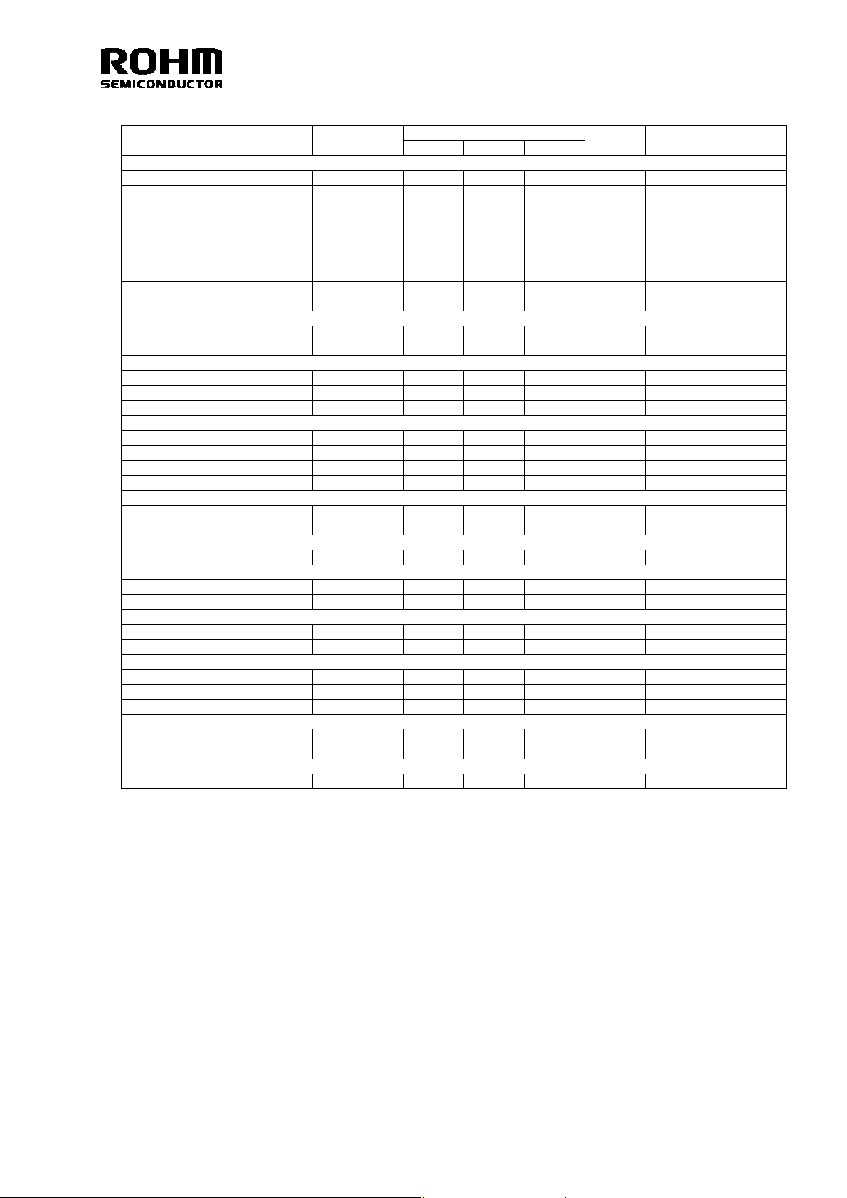
○ ABSOLUTE MAXIMUM RATINGS(Ta=25℃)
Parameter Symbol Limit Unit
Input Voltage 1 VCC 7
Input Voltage 2 VDD 7
Input Voltage 3 VIN 28
BOOT Voltage BOOT 35
BOOT-SW Voltage BOOT-SW 7
HG-SW Voltage HG-SW 7
LG Voltage LG VDD V
Output Voltage VOUT/Is+/Is- VCC V
EN Input Voltage EN 7
Power Dissipation 1 Pd1 0.34
Power Dissipation 2 Pd2 0.70
Power Dissipation 3 Pd3 2.20
Power Dissipation 4 Pd4 3.56
Operating Temperature Range Topr -10~+100 ℃
Storage Temperature Range Tstg -55~+150 ℃
Maximum Junction Temperature Tjmax +150 ℃
*1 Not to exceed Pd.
*2 Instantaneous surge voltage, back electromotive force and voltage under less than 10% duty cycle.
*3 Reduced by 2.7mW/℃ for each increase in Ta of 1℃ over 25℃. (when don’t mounted on a heat radiation board )
*4 Reduced by 5.6mW/℃ for increase in Ta of 1℃ over 25℃. (when mounted on a board 70.0mm×70.0mm×1.6mm 1-layer Glass-epoxy PCB,
copper foil area: 10.29mm
*5 Reduced by 17.6mW/℃ for increase in Ta of 1℃ over 25℃. (when mounted on a board 70.0mm×70.0mm×1.6mm 4-layer Glass-epoxy PCB,
copper foil area: 10.29mm
*6 Reduced by 28.5mW/℃ for increase in Ta of 1℃ over 25℃. (when mounted on a board 70.0mm×70.0mm×1.6mm 4-layer Glass-epoxy PCB,
copper foil area: 5505mm
2
)
2
2,3-layer copper foil area: 5505mm2)
2
)
○ OPERATING CONDITIONS(Ta=25℃)
Parameter Symbol MIN MAX Unit
Input Voltage 1 VCC 4.5 5.5 V
Input Voltage 2 VDD 4.5 5.5 V
Input Voltage 3 VIN 4.5 25 V
BOOT Voltage BOOT 4.5 30 V
SW Voltage SW -0.7 25 V
BOOT-SW Voltage BOOT-SW 4.5 5.5 V
EN Input Voltage EN 0 5.5 V
Is Input Voltage Is+/Is- 0.7 2.7 V
MIN ON Time Tonmin - 80 ns
★ This product is not designed for protection against radioactive rays.
2
*1*
V
2
*1*
V
2
*1*
V
2
*1*
V
2
*1*
V
2
*1*
V
1
*
V
3
*
W
4
*
W
5
*
W
6
*
W
REV. A
2/4
[
[
p
_
[
[
[
p
[
p
[
[
[
]
[
[
○ELECTRICAL CHARACTERISTICS (unless otherwise noted, Ta=25℃ VCC=5V,VDD=5V,EN=3V,VIN=12V,VOUT=1.05V,RFS=36kΩ)
Parameter Symbol
Standard Value
MIN TYP MAX
Unit Condition
Whole Device]
VCC Bias Current
VCC Standby Current
VIN Bias Current
VIN Standby Current
EN Low Voltage
EN HighVoltage
(Forced Continuous mode)
EN HighVoltage (SLLM Mode)
EN Bias Current
Icc
Iccstb
Iin
Iinstb
EN_low
V
V
ENth_con
ENth_sllm
V
Ien
- 1500 1800 μA
-010μA EN=0V
-3080μA
-010μA EN=0V
GND - 0.8 V
2.3 - 3.8 V
4.5 - 5.5 V
-1525μA EN=3V
Under Voltage Locked Out ]
VCC threshold voltage Vcc_UVLO 3.7 4.0 4.3 V VCC:Sweep u
VCC hysteresis voltagedVcc
UVLO 100 160 220 mV VCC:Sweep down
H3REG Control]
ON Time Ton 194 219 244 ns
MAX ON Time Tonmax - 3.5 -
μs
MIN OFF Time Toffmin - 490 700 ns
FET Driver]
HG Higher side ON resistor HGhon - 3.0 6.0 Ω
HG Lower side ON resistor HGlon - 2.0 4.0 Ω
LG Higher side ON resistor LGhon -
3.0 6.0
Ω
LG Lower side ON resistor LGlon - 0.5 1.0 Ω
SCP]
SCP strat-up Voltage Vsc
0.345 0.420 0.495
SCP delay time Tscp - 2.5 - ms
V
OVP]
FB threshold voltage Vov
0.825 0.900 0.975
V
Soft start]
Charge current Iss 1 2 3 μA
Standby voltage Vss_stb - - 50 mV
Current Limit Block]
Setting Current Iilim - 10 -
μA
Current limit threshold Ilim 75 100 125 mV RILIM=100kΩ
Output Voltage setting
VOUT typical voltage
REF 0.743 0.750 0.757 V
Is+ Input current IIs+ -1 0 1 μA Is+=1.05V
Is- Input current IIs- -1 0 1 μA Is-=1.05V
Power Good]
FB Power Good V
PGOOD
0.38 0.47 0.56
V
Discharge ON resistor Ronpgood - 50 150 Ω
BOOT Diode]
VF voltage
VF 0.4 0.5 0.6 V IF=1mA
REV. A

3/4
○ PHYSICAL DIMENSIONS ○ Pin Number Pin Name
C0.2
○ BLOCK DIAGRAM
EN/SLLM
OUT
4.0
±0.1
4.0
1.0Max.
0.08 S
2.1±0.1
15
20
0.4±0.1
16
1.0
0.5
2
REF×0.56
SS×0.56
VOUT
18
FB
5
SS
REF
7
FREQ
±0.1
95371
Lot.No
1pin mark
S
-0.02
+0.03
(0.22)
0.02
6
2.1±0.1
10
1115
+0.05
0.25
-0.04
VQFN020V4040 (Unit:mm)
VDD
CC
V
4
Reference
Block
FB
EN/UVLO
+
+
9
ls-
BG
REF
+
10
Is+ VOUT
+
-
BG
2.5ms Delay
ls+
+
-
UVLO
UVLO
SCP
H3RegTM
Controller
Block
ILIM
SCP
TSD
VIN
17
VIN
EN
FS
Thermal
Protection
+
ILIM
8
TSD
SLLM
REF×1.2
FB
Q
R
S
Current Limit
+
Is+
6
Pin
number
PIN name
1 SS
2 EN/SLLM
3 ILIM
4 VCC
5 FB
6 VOUT
7 FREQ
8 FS
9 Is10 Is+
11 PGND
12 LG
13 VDD
14 SW
15 HG
16 BOOT
17 VIN
18 OUT
19 PGOOD
20 GND
reverse FIN
Please connect FIN to GND.
1
+
SLLM
SLLM
3
SS
Soft Start Block
OVP
×0.56
ILIM
REF
20
SS
Driver
Circuit
OVP
FB
GND
VDD
PGND
+
-
BOOT
HG
SW
VDD
LG
16
15
14
13
12
11
19
PGOOD
VIN
VOUT
REV. A
4/4
●Operation Notes
1. Absolute maximum ratings
An excess in the absolute maximum ratings, such as supply voltage, temperature range of operating conditions, etc.,
can break down the devices, thus making impossible to identify breaking mode, such as a short circuit or an open circuit.
If any over rated values will expect to exceed the absolute maximum ratings, consider adding circuit protection devices,
such as fuses.
2. Connecting the power supply connector backward
Connecting of the power supply in reverse polarity can damage IC. Take precautions when connecting the power
supply lines. An external direction diode can be added.
3. Power supply lines
Design PCB layout pattern to provide low impedance GND and supply lines. To obtain a low noise ground and supply
line, separate the ground section and supply lines of the digital and analog blocks. Furthermore, for all po wer supply
terminals to ICs, connect a capacitor between the power supply and the GND terminal. When applying electrolytic
capacitors in the circuit, not that capacitance characteristic values are reduced at low temperatures.
4. GND voltage
The potential of GND pin must be minimum potential in all operating conditions.
5. Thermal design
Use a thermal design that allows for a sufficient margin in light of the power dissipation (Pd) in actual operating
conditions.
6. Inter-pin shorts and mounting errors
Use caution when positioning the IC for mounting on printed circuit boar ds. The IC may be damaged if there is any
connection error or if pins are shorted together.
7. Actions in strong electromagnetic field
Use caution when using the IC in the presence of a strong e lectromagnetic field as doing so may cause the IC to
malfunction.
8. ASO
When using the IC, set the output transistor so that it does not exceed absolute maximum ratings or ASO.
9. Thermal shutdown circuit
The IC incorporates a built-in thermal shutdown circuit (TSD circuit). The thermal shutdown circuit (TSD circuit) is
designed only to shut the IC off to prevent thermal runaway. It is not designed to protect the IC or guarantee its
operation. Do not continue to use the IC after operating this circuit or use the IC in an environment where the operation
of this circuit is assumed.
10. Ground Wiring Pattern
When using both small signal and large current GND patterns, it is recommended to isolate the two ground patterns,
placing a single ground point at the ground potential of a pplication so that the pattern wiring resistance and voltage
variations caused by large currents do not cause variations in the small signal ground voltage. Be careful not to change
the GND wiring pattern of any external components, either.
11. Heat sink (FIN)
Since the heat sink (FIN) is connected with the Sub, short it to the GND.
TSD on temperature [°C] (typ.) Hysteresis temperature [°C](typ.)
BD95371MUV 175 15
REV. A

Notes
No copying or reproduction of this document, in part or in whole, is permitted without the
consent of ROHM Co.,Ltd.
The content specied herein is subject to change for improvement without notice.
The content specied herein is for the purpose of introducing ROHM's products (hereinafter
"Products"). If you wish to use any such Product, please be sure to refer to the specications,
which can be obtained from ROHM upon request.
Examples of application circuits, circuit constants and any other information contained herein
illustrate the standard usage and operations of the Products. The peripheral conditions must
be taken into account when designing circuits for mass production.
Great care was taken in ensuring the accuracy of the information specied in this document.
However, should you incur any damage arising from any inaccuracy or misprint of such
information, ROHM shall bear no responsibility for such damage.
The technical information specied herein is intended only to show the typical functions of and
examples of application circuits for the Products. ROHM does not grant you, explicitly or
implicitly, any license to use or exercise intellectual proper ty or other rights held by ROHM and
other parties. ROHM shall bear no responsibility whatsoever for any dispute arising from the
use of such technical information.
Notice
The Products specied in this document are intended to be used with general-use electronic
equipment or devices (such as audio visual equipment, ofce-automation equipment, communication devices, electronic appliances and amusement devices).
The Products specied in this document are not designed to be radiation tolerant.
While ROHM always makes efforts to enhance the quality and reliability of its Products, a
Product may fail or malfunction for a variety of reasons.
Please be sure to implement in your equipment using the Products safety measures to guard
against the possibility of physical injury, re or any other damage caused in the event of the
failure of any Product, such as derating, redundancy, re control and fail-safe designs. ROHM
shall bear no responsibility whatsoever for your use of any Product outside of the prescribed
scope or not in accordance with the instruction manual.
The Products are not designed or manufactured to be used with any equipment, device or
system which requires an extremely high level of reliability the failure or malfunction of which
may result in a direct threat to human life or create a risk of human injury (such as a medical
instrument, transportation equipment, aerospace machinery, nuclear-reactor controller, fuelcontroller or other safety device). ROHM shall bear no responsibility in any way for use of any
of the Products for the above special purposes. If a Product is intended to be used for any
such special purpose, please contact a ROHM sales representative before purchasing.
If you intend to export or ship overseas any Product or technology specied herein that may
be controlled under the Foreign Exchange and the Foreign Trade Law, you will be required to
obtain a license or permit under the Law.
Thank you for your accessing to ROHM product informations.
More detail product informations and catalogs are available, please contact us.
ROHM Customer Support System
www.rohm.com
© 2010 ROHM Co., Ltd. All rights reserved.
http://www.rohm.com/contact/
R1010
A
 Loading...