

Page 1
LED Driver series for lighting
Step-down type
with 1.5A output
BD9207FPS
No.09093EAT01
●Description
BD9207FPS is a LED driver with built-in step-down switching regulator and incorporates the bui lt-in switching MOS EFT of
Pch.
Feedback voltage is as low as 0.2V and can suppress the loss on the sense resistance of LED.
It is operated by PWM method with an oscillating frequency of 900 KHz and can use smaller coil than a switching regulator
of low-frequency operation.
●Features
1) Maximum switching current of 1.5A
2) Built-in Pch switching MOS FET for high efficiency
3) Low loss because feedback voltage is as low as 0.2V
4) High oscillating frequency of 900KHz (Fixed)
5) Built-in soft start function
6) Built-in overcurrent protection circuit (OCP)
7) Built-in thermal shutdown circuit (TSD)
8) ON/OFF of output is possible by STBY terminal.
9) Compact surface-mount TO252S-5 package
●Applications
・For use in the light sources of PPC
・Printer etc. and the LCD backlights of LED lighting apparatus & monitor
・Note PC etc.
●Absolute maximum ratings(Ta=25℃)
Parameter Symbol
Supply voltage(VCC-GND) Vcc 36 V
STBY-GND Voltage V
OUT-GND Voltage V
INV-GND Voltage V
Maximum switching output current. Iout 1.5(*1) A
Allowable loss Pd 800(*2) mW
Operating temperature range Topr -20 ~ +85 ℃
Storage temperature range Tstg -55 ~ +150 ℃
(*1)Regardless of the listed rating, do not exceeded Pd, ASO or Tjmax=150℃.
(*2) Without heat sink, reducing by the 16 mW every 1℃ rise in temperature. (above 25℃)
36 V
STBY
36 V
OUT
5 V
INV
Rating Unit
www.rohm.com
1/11
© 2009 ROHM Co., Ltd. All rights reserved.
2009.07 - Rev.A
Page 2

BD9207FPS
●Operating range (Ta=-40~+85℃)
Parameter Symbol
Supply voltage VCC 8.0 - 35.0 V
Output voltage Vo 2.5 -
●Electrical characteristics(Unless otherwise specified, Ta=25℃,VCC=24V,STBY=3V)
Parameter Symbol
Output MOS ON resistance Ron - 1.0 1.5 Ω
Oscillating frequency fosc 810 900 990 kHz
Overcurrent detection current Iocp 1.6 - - A
INV terminal threshold
voltage
INV terminal bypass current IINV - 1 2 μA
STBY terminal control
voltage
STBY terminal inflow current Istby 5 15 30 μA
Circuit current Icc - 5 12 mA
Standby current Ist - 0 5 μA
Soft start time Tss - - 10 ms
Without radiation-proof design.
ON VSTBYON 2.0 - 36 V
OFF VSTBYOFF -0.3 - 0.3 V
Min. Typ. Max.
VINV 0.194 0.200 0.206 V
Limit
0.8×
(VCC-Io×Ron)
Limit
Min. Typ. Max.
Unit Conditions
V
Technical Note
Unit Conditions
VINV=0.2V
STBY=3V
STBY=0V
STBY=0→3V
www.rohm.com
2/11
© 2009 ROHM Co., Ltd. All rights reserved.
2009.07 - Rev.A
Page 3
BD9207FPS
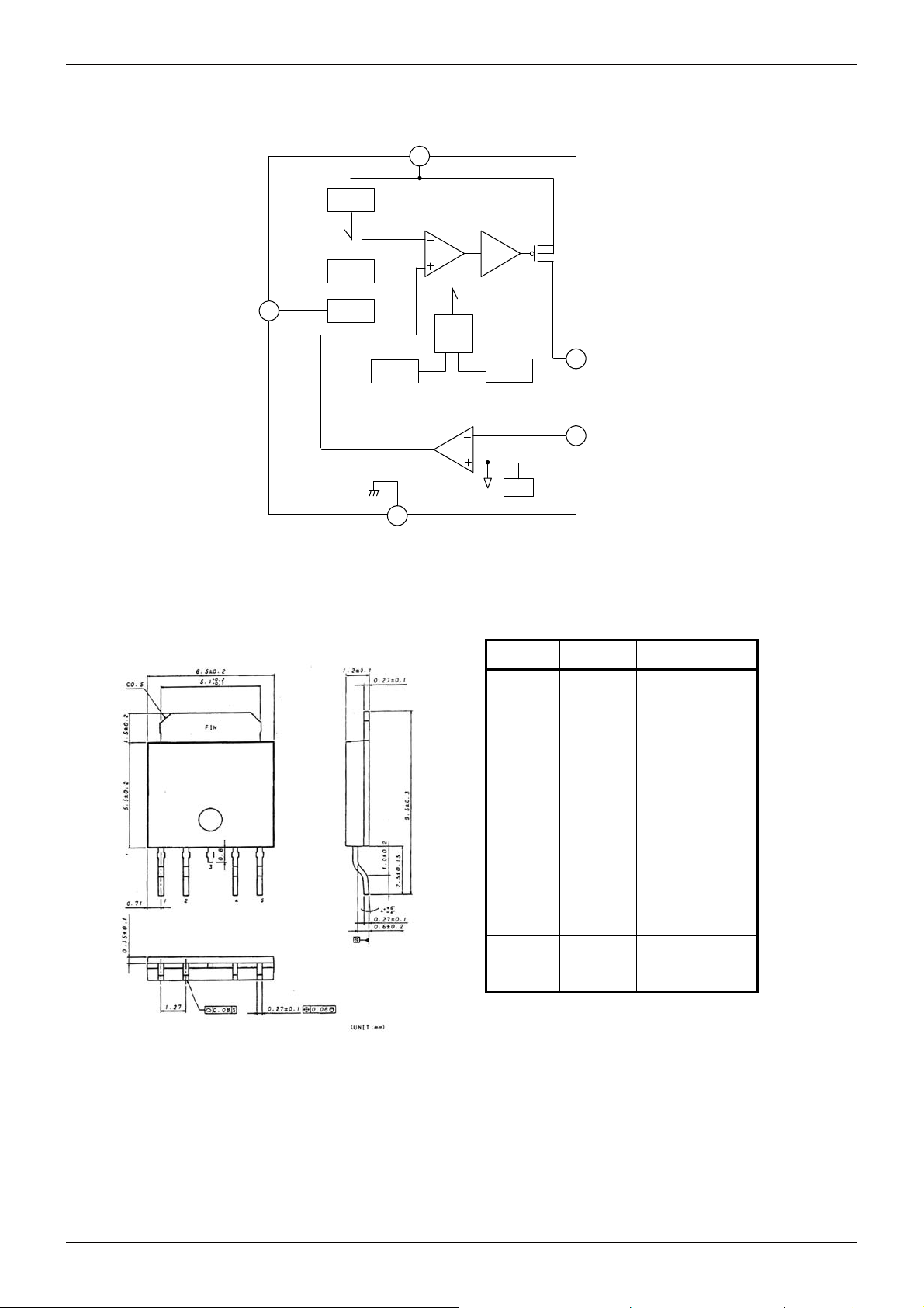
●Block diagram
VCC
1
VREF
PWM COMP
DRIVER
STBY
5
OSC
STBY
TSD
CTL
LOGIC
OUT
2
OCP
Error AMP
INV
4
SS
FIN
GND
●Outline drawing of package ●Explanation of terminal
Pin No. Pin Name Function
1 VCC
2 OUT
3※
OUT
FIN GND Ground terminal
4 INV
5 STBY
※Used normally in open-circuit condition
TO252S-5(Unit:mm)
Technical Note
Supply voltage
terminal
Drain terminal of
built-in PMOS FET
Drain terminal of
built-in PMOS FET
Output voltage
feedback
terminal
ON/OFF control
terminal
www.rohm.com
3/11
© 2009 ROHM Co., Ltd. All rights reserved.
2009.07 - Rev.A
Page 4

BD9207FPS
●Functional explanation of block
・ VREF
The constant voltage to be temperature-compensated is created from the voltage inputted from VCC terminal.
・ OSC
Triangular wave with an oscillating frequency of 900 KHz is created, as an input of PWM comparator, by built-in resistor
and capacitor.
・ Error AMP
It detects, at INC terminal, the voltage of sense resistance terminal created by LEC current, and compares it to the
reference voltage, and amplifies and outputs the differential voltage.
(The reference voltage is 0.2V±3%)
・ PWM COMP
PWM COMP converts the output voltage of error amplifier into the pu lse-width modulation waveform and outputs it to
DRIVER.
・ DRIVER
Push-pull FET driver takes in the PWM waveform and directly drives the Pch MOS FET that is built-in in the IC.
・ STBY
The ON/OFF control of output is performed by STBY terminal. The output becomes ON if STBY voltage is High level.
・ Thermal shutdown circuit (TSD)
TSD circuit protects the IC from runaway thermal operation or heat damage.
TSD circuit detects the temperature of chip, and the circuit becomes off if the temperature reaches 175℃. For TSD
detection and release, the hysteresis of 15℃ is set, so the malfunction caused by temperature variation is prevented.
・ Over Current Protection(OCP)
Out is turned off if the voltage difference between VCC – OUT, caused by the current flowing in the Pch MOS EFT built-in
in OCP circuit, is detected and reaches the reference value of OCP. The OCP is not of latch type but of self-return type.
・ Soft start circuit (SS)
Soft start time is set by the built-in capacitor connected to SS circuit. The capacitor is charged when STBY terminal
becomes High level and the IC is started. The soft start time is set at 4ms or so.
Technical Note
www.rohm.com
4/11
© 2009 ROHM Co., Ltd. All rights reserved.
2009.07 - Rev.A
Page 5

BD9207FPS
Technical Note
●Selection and setting of application parts
Coil L1
The application efficiency will decrease by the larger serial resistance element of coil. Moreover, because OCP operates
by 1.6A(min) or more, so please notice the heat generated by overload output or short.
Please set current ratings of coil with I
(MAX)+⊿IL or more. Iout(MAX): maximum load current
OUT
If current flows more than ratings current, then coil generates heat, magnetic saturation, and causes oscillation or lo w
efficiency.
Please select the peak current with enough margins not to exceed current rating of coil.
⊿IL
(VCC-VOUT)
=
.
L1
VOUT
× ×
VCC
1
fosc
L1: Coil value,VCC: Input voltage,VOUT: Output voltage, ⊿IL: Ripple current, fosc: Oscillation frequency
When value the efficiency , we recommend C10-H5R(mitsumi) . Efficiency will be improved about 1~2%.
Schottky diode D1
Please select Schottky diode with lowest forward voltage VF.
(We can suppress the dissipation of forward voltage descent, and raise the efficiency. )
Diode selection is based on maximum forward current rating, reverse voltage rating and permissible power dissi pation of
diode.
・The maximum current ratings are assumed more than the value of maximum load current+ coil ripple current(⊿I
・Reverse voltage rating is set to be VIN or more.
・Please choose the smallest one of reverse current IR.
Especially, IR grows at high temperature, and causes thermo runaway.
・Select the diode which permissible power dissipation within ratings.
Diode power dissipation Pdi is shown below.
Pdi=Iout(MAX)×Vf×(1-VOUT/VCC)
Iout(MAX): Load current. Vf: Forward voltage, VOUT: Output voltage, VCC: Input voltage
Output capacitor C1
Select the output capacitor with ESR met the following formula.
ESR≦⊿VL/⊿IL
⊿VL : Permissible ripple voltage, ⊿IL : Ripple current
Moreover, permissible ripple current effective value of output capacity is calculated by the next formula, and use this
value to select the capacitor with enough margins.
IRMS =⊿IL/2
√3
IRMS: Permissible ripple current effective value of output capacity, ⊿IL : Ripple current
Ceramic capacitor must use the one more than B characteristic.
Besides above mentioned, IC might not be normally operated according to the different setting condition of ambient
temperature and output voltage.
Moreover, even aluminum electrolytic capacitor can be used, please confirm its operation enough before using it.
Input capacitor C2
Input capacitor built in Pch MOS FET ON is the current supply of coil by FET.
So, please close to IC as near as possible to connect it. Enough margins is taken on setting input capacitor in capacitor
withstand voltage and permissible ripple current value. According to the ripple current effective value of input capacitor
shown below, select the capacitor with enough permissible ripple current value.
IRMS=IOUT×√
(1-VOUT / VCC)×VOUT / VCC
IRMS : Permissible ripple current value of input capacitor
IOUT : Load current. VOUT: Output voltage, VCC: Input voltage
).
L
www.rohm.com
5/11
© 2009 ROHM Co., Ltd. All rights reserved.
2009.07 - Rev.A
Page 6

BD9207FPS
Resistance R1
LED Current value is set below according to sense resistance R1.
ILED[A]=VINV[V]/R1[Ω]
=0.2V/R1[Ω]
Moreover, DCDC Output voltage will be the value below.
VO[V]=VF(LED Forward voltage)+VINV[V]
=VF+0.2V(typ)
● Recommended circuit example and notes of substrate layout
・ To prevent noise and low efficiency, please set up the capacitor and Schottky diode between VCC – GND as near as
possible to IC.
・ Please connect the resistance and output LC filter capacitor between INV – GND with same GND for the stability of
output voltage.
<Recommended parts example>
Coil L1=10μH :C6-K3LA(mitsumi)
Diode D1 :RB050LA-30(ROHM)
Capacitor C1=10μF(25V) :Ceramic capacitor GRM31CB31E106KA75L(murata)
C2=4.7μF(50V) :Ceramic capacitor GRM32EB31H475KA87L(murata)
Resistance R1=0.43Ω :MCR10EZPFR430
(ROHM)
Technical Note
www.rohm.com
6/11
© 2009 ROHM Co., Ltd. All rights reserved.
2009.07 - Rev.A
Page 7

BD9207FPS
● Measurement circuit diagram
+
Icc
Vcc
Vcc
1
cccc
A
Technical Note
OUT
2
SW2
f
GND
FIN
0.43Ω
INV
STBY
45
SW4 SW5
A
IINV
V
+
INV
V
A
ISTB
VSTB
SW6
Vo
Io
www.rohm.com
7/11
© 2009 ROHM Co., Ltd. All rights reserved.
2009.07 - Rev.A
Page 8

BD9207FPS
● Heat transfer characteristic
①IC unit
②2 layers substrate(area of substrate back copper foil:15 mm×15mm)
③2 layers substrate(area of substrate back copper foil:70 mm×70mm)
(W)
5
4
③3.50W
3
2
②1.85W
POWER DISSIPATION [Pd]
①0.80W
1
0
0 25 50 75 100 125
85
AMBIENT TEMPERA TURE [Ta]
150
(℃)
● I/O terminal equivalent circuit diagram
1Pin,FIN (VCC, GND) 2pin (OUT) 4pin (INV) 5pin (STBY)
VCC
GND
VCC
OUT
VCC
INV
STBY
Technical Note
VCC
www.rohm.com
8/11
© 2009 ROHM Co., Ltd. All rights reserved.
2009.07 - Rev.A
Page 9

BD9207FPS
●Notes for use
1. We have paid enough attention to quality control of this product, but it may be destroyed when the absolute
maximum rating of impressed voltage and operating temperature range is exceeded. Because we can’t specif y
that is short-mode or open-mode etc while it is destroyed, so please discuss to give physical safety action with
postulating the special mode exceeded absolute maximum rating.
2. About application circuit
Application circuit is recommended, but please fully confirm temperature characteristic etc when using it. Moreover,
please acknowledge that our company can’t confirm enough about patent.
3. About the range of operation power-supply voltage
Circuit function operation at the range of operation ambient temperature i s guaranteed when it is in the range of
operation power-supply voltage. About characteristic value, the specification value of electric characteristic can’t
be guaranteed, but the characteristic value doesn’t change rapidly in thes e ranges.
4. About ground connection
The ground connection shown in application circuit example should equip enough fat GND(FIN) to every ground
connection with shortest pattern drawing, and the pattern shouldn’t interfere the electric characteristic.
5. About input power-supply
The input power-supply shown in application circuit exampl e should equip input pin VCC(1pin) with sho rt enough
pattern drawing, and the pattern shouldn’t interfere the electric characteristic.
6. Please think about permissible power dissipation (Pd) in an actual using status, and do the heat design with
enough margins.
7. Please pay enough attention to the direction and displacement of IC when you install it on PCB. If you install it by
mistake, IC might be destroyed, Moreover, when short-circuit happen by foreign substance entered between
outputs, or output and power supply GND, it will be destroyed.
8. Please note that there is a possibility of malfunction if you use it in strong electromagnetic field.
9. Please set STBY terminal voltage to 0.3V or less when putting it on standby status, to 2.0V or more when putting it
on operation status.
Please do not fix STBY terminal voltage from 0.3V to 2.0V. It may cause malfunction or breakdown.
Technical Note
www.rohm.com
9/11
© 2009 ROHM Co., Ltd. All rights reserved.
2009.07 - Rev.A
Page 10

BD9207FPS
~
~
Technical Note
10. This IC is a monolithic IC, and there are P + isolation and P substrate for element separation between each
element. P-N joint is formed with this P layer and N each element’s layer, and various parasitic elements are
composed.
For instance, as shown in the figure below, when resistance and transistor are connected with terminal:
○ P-N joint operates as a parasitic diode when GND > (terminal A) in resistance, GND >(terminal B) in transistor
(NPN).
○ Moreover, when GND > (terminal B) in transistor (NPN),the parasitic NPN transistor operates with N layer of other
elements adjoining with above-mentioned parasitic diode.
According to potential relation, parasitic element in IC structure can be consequent. The operating of parasitic
element maybe interfere the circuit operation, and become the cause of malfunction and destruction. Therefore,
please pay enough attention not to use it by impressing lower voltage than GND (P substrate) on I/O terminal etc
to operate parasitic element.
(TerminalA)
N N
Psubstrate
Resistance
P
N
(TerminalB)
~
~
+
P+
P
Parasitic element
Transistor(NPN)
B
C
E
~
~
N
P
P
+
P+
N
N N
Psubstrate
GND
GND
GND
Parasitic element
(TerminalB)
(TerminalA)
~
~
Parasitic element
B
C
E
GND
other adjoining elements
GND
Parasitic element
Simple structure example of bipolar IC
www.rohm.com
10/11
© 2009 ROHM Co., Ltd. All rights reserved.
2009.07 - Rev.A
Page 11

BD9207FPS
●Ordering part number
B D 9 2 0 7 F P S - E 2
Part No. Part No.
TO252S-5
C0.5
6.5±0.2
+0.2
5.1
−0.1
FIN
1.5±0.2
5.5±0.2
0.71
3
0.8
2
1
1.27
0.35±0.1
0.08 S
54
0.27±0.1
1.2±0.1
S
0.08
0.27±0.1
1.0±0.2
+6
4
–4
0.27±0.1
0.6±0.2
M
9.5±0.3
2.5±0.15
(Unit : mm)
Package
FPS: TO252S-5
<Tape and Reel information>
Embossed carrier tapeTape
Quantity
Direction
of feed
2000pcs
E2
The direction is the 1pin of product is at the lower left when you hold
( )
reel on the left hand and you pull out the tape on the right hand
Reel
Packaging and forming specification
E2: Embossed tape and reel
1pin
Order quantity needs to be multiple of the minimum quantity.
∗
Technical Note
Direction of feed
www.rohm.com
11/11
© 2009 ROHM Co., Ltd. All rights reserved.
2009.07 - Rev.A
Page 12

Notes
No copying or reproduction of this document, in part or in whole, is permitted without the
consent of ROHM Co.,Ltd.
The content specied herein is subject to change for improvement without notice.
The content specied herein is for the purpose of introducing ROHM's products (hereinafter
"Products"). If you wish to use any such Product, please be sure to refer to the specications,
which can be obtained from ROHM upon request.
Examples of application circuits, circuit constants and any other information contained herein
illustrate the standard usage and operations of the Products. The peripheral conditions must
be taken into account when designing circuits for mass production.
Great care was taken in ensuring the accuracy of the information specied in this document.
However, should you incur any damage arising from any inaccuracy or misprint of such
information, ROHM shall bear no responsibility for such damage.
The technical information specied herein is intended only to show the typical functions of and
examples of application circuits for the Products. ROHM does not grant you, explicitly or
implicitly, any license to use or exercise intellectual property or other rights held by ROHM and
other par ties. ROHM shall bear no responsibility whatsoever for any dispute arising from the
use of such technical information.
Notice
The Products specied in this document are intended to be used with general-use electronic
equipment or devices (such as audio visual equipment, ofce-automation equipment, communication devices, electronic appliances and amusement devices).
The Products specied in this document are not designed to be radiation tolerant.
While ROHM always makes efforts to enhance the quality and reliability of its Products, a
Product may fail or malfunction for a variety of reasons.
Please be sure to implement in your equipment using the Products safety measures to guard
against the possibility of physical injury, re or any other damage caused in the event of the
failure of any Product, such as derating, redundancy, re control and fail-safe designs. ROHM
shall bear no responsibility whatsoever for your use of any Product outside of the prescribed
scope or not in accordance with the instruction manual.
The Products are not designed or manufactured to be used with any equipment, device or
system which requires an extremely high level of reliability the failure or malfunction of which
may result in a direct threat to human life or create a risk of human injury (such as a medical
instrument, transpor tation equipment, aerospace machinery, nuclear-reactor controller,
fuel-controller or other safety device). ROHM shall bear no responsibility in any way for use of
any of the Products for the above special purposes. If a Product is intended to be used for any
such special purpose, please contact a ROHM sales representative before purchasing.
If you intend to export or ship overseas any Product or technology specied herein that may
be controlled under the Foreign Exchange and the Foreign Trade Law, you will be required to
obtain a license or permit under the Law.
Thank you for your accessing to ROHM product informations.
More detail product informations and catalogs are available, please contact us.
ROHM Customer Support System
www.rohm.com
© 2009 ROHM Co., Ltd. All rights reserved.
http://www.rohm.com/contact/
R0039
A
 Loading...