

LED Driver Series for LCD Backlight
Simple Structure Constant Current
Backlight Driver for LCD panels
(Non-step type)
BD9206EFV
No.09040EAT03
●Description
BD9206EFV is an IC with a built-in 6ch high-accuracy (absolute accuracy:±4%) constant-current driver.
Capable of lighting a maximum of 36 white LEDs with 6 rows×6 lines.
Due to the wide input voltage range (8V~30V), it can be widely used from a backlights of Note PC and PDA etc. to LED light
sources of Scanner and PPC etc.
Moreover, it restrain the generation of heat at the time of large current drive because of adoption of high-heat-radiation
package(HTSSOP-B20).
●Features
1) A wide input voltage range(8V~30V)
2) Capable of driving a maximum of 36 white LEDs of 6 series×6 parallel
3) Value of constant current is set by the VSET terminal
4) Due to the STBY terminal, the consumption current at the time of standby is low
5) PWM dimming is possible due to the clock input to the EN terminal
6) Built-in 5V regulator
7) High-heat-radiation package of HTSSOP-B20 6.4×6.5×0.85mm
●Applications
For use in LED light source of PPC and Scanner etc., LED lighting fixture, and LCD backlight lights of monitor
and note PC etc.
●Absolute maximum ratings(Ta=25℃)
Item Symbol Rating Unit
Power Supply Voltage Vcc 36 V
V
LED output voltage
Power Dissipation Pd 3.2
Operational Temperature Range
Storage Temperature Range Tstg -55~+150 ℃
LED Maximum Current
*1 Reduce with 25.6mW at 1℃ if Ta= 25℃ or above at the time of mounting a base-plate of glass
epoxy in 4 layer of 70mm×70mm×1.6mm.
*2 It is value per LED driver 1ch.
Please set inside the range which does not exceed the allowable loss value of the package.
LED 28 V
Topr -40~+85 ℃
I
LED 30
*1
W
*2
mA
www.rohm.com
1/12
© 2009 ROHM Co., Ltd. All rights reserved.
2009.07 - Rev.A

BD9206EFV
●Recommended Operational condition(Ta=25℃)
Item
Power Supply Voltage
EN terminal clock input possible range VENCLK 100~10000 Hz
VSET input possible range VSET 0.6~3 V
Applied voltage range for LED terminal VLED 0.6~28 V
●Electrical Characteristics(Unless specified, Ta=25℃,Vcc=24V)
Item Symbol
【Whole】
Circuit electric current
when OFF
Circuit electric current
when stand by
Circuit electric current
when operating
【LED Driver 1~6】
IOFF - 17 28 μA STBY=L, EN=L, TEST=L
ST - 1.8 3.6 mA STBY=H, EN=L, TEST=L
I
ICC - 2.5 5.0 mA STBY=H, EN=H, TEST=L
Symbol Rating Unit
Vcc 8~30 V
Ratings
Min.
Typ.
Technical Note
Unit Conditions
Max.
Output current ILED 19.2 20.0 20.8 mA VSET=2.0V, VLED=1V
Leak electric current
when OFF
Influx electric current to
VSET terminal
【VREG】
Output voltage VREG 4.7 5.0 5.3 V Io=1mA
Output current IOMAX 10 30 - mA Vo=VREG×0.9
【UVLO】
Detection voltage VUVREG 2.4 2.9 3.4 V VREG fall down
Hysteresis voltage VUHYVREG 0.05 0.1 0.2 V VREG rise up
【STBY, EN, TEST】
Input Low level VIL -0.3 - 0.8 V
Input high level VIH 2.0 - Vcc V
Input current RPD 33 47 66 μA Vin=3V
It is not the radiation-proof design for this product.
ILEDLK - 0.0 5.0 μA VLED=26V
INVSET - -0.05 -0.10 μA VSET=2V
I
www.rohm.com
2/12
© 2009 ROHM Co., Ltd. All rights reserved.
2009.07 - Rev.A
BD9206EFV
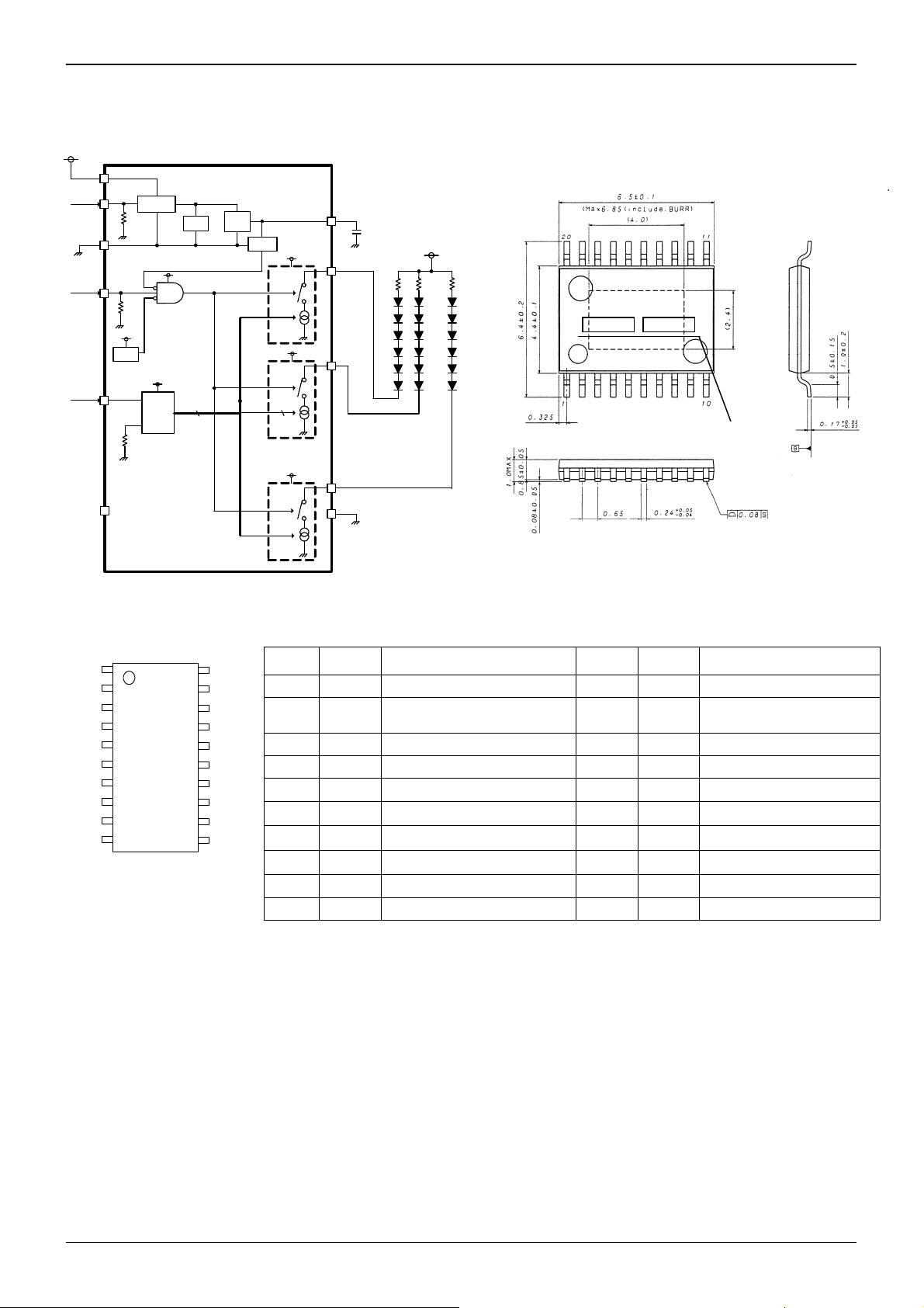
●Block diagram ●Package outline drawing
VCC
20
STBY
2
PREREG
AGND
100k
4
5VREG
Driver
Current
Setting
5VREG
EN
3
VSET
100k
PREREG
TSD
18
RSET
REF
5V
REG
UVLO
5VREG
ENH1
ISET1
5VREG
6
ISET2~5
4
Current
Driver
1
6
LED2~5
VREG
Vo
LED1
BD9206EFV
・・・・
ISET6
5VREG
・・・・ ・
LED6
15
PGND1~2
HTSSOP-B20(Unit:mm)
17
TEST
●Terminal placement diagram ●Terminal explanation
VREG
1
2
STBY
EN
3
4
AGND
5
PGND1
6
LED1
LED2
7
LED3
8
N.C.
9
N.C.
10
Fig..3
Fig..1 Fig..2
Terminal
VCC
20
19
N.C.
18
VSET
TEST
17
PGND2
16
15
LED6
LED5
14
13
LED4
12
N.C.
11
N.C.
number
Terminal
name
Function
Terminal
number
Terminal
name
1 VREG Power supply for internal circuit 11 N.C. (Not yet connected terminal)
2 STBY
Stand by terminal
(Low:OFF,High:stand by,
operation)
12 N.C. (Not yet connected terminal)
3 EN LED1~16 Enable terminal(Active:High) 13 LED4 Output terminal 4 for LED driver
4 AGND
GND for internal standard section 14 LED5 Output terminal 5 for LED driver
5 PGND1 POWER GND for LED driver 15 LED6 Output terminal 6 for LED driver
6 LED1
Output terminal 1 for LED driver 16 PGND2
7 LED2 Output terminal 2 for LED driver 17 TEST
8
9 N.C.
LED3 Output terminal 3 for LED driver 18 VSET
(Not yet connected terminal) 19 N.C. (Not yet connected terminal)
10 N.C. (Not yet connected terminal) 20 VCC Terminal of power supply
Technical Note
Lot No.
Function
Power GNDPOWER GND for LED
driver
Terminal for test mode shift
(Use at usual time:Low)
Standard voltage terminal for fixed
electric current setting
www.rohm.com
3/12
© 2009 ROHM Co., Ltd. All rights reserved.
2009.07 - Rev.A
BD9206EFV
(
)
(
)
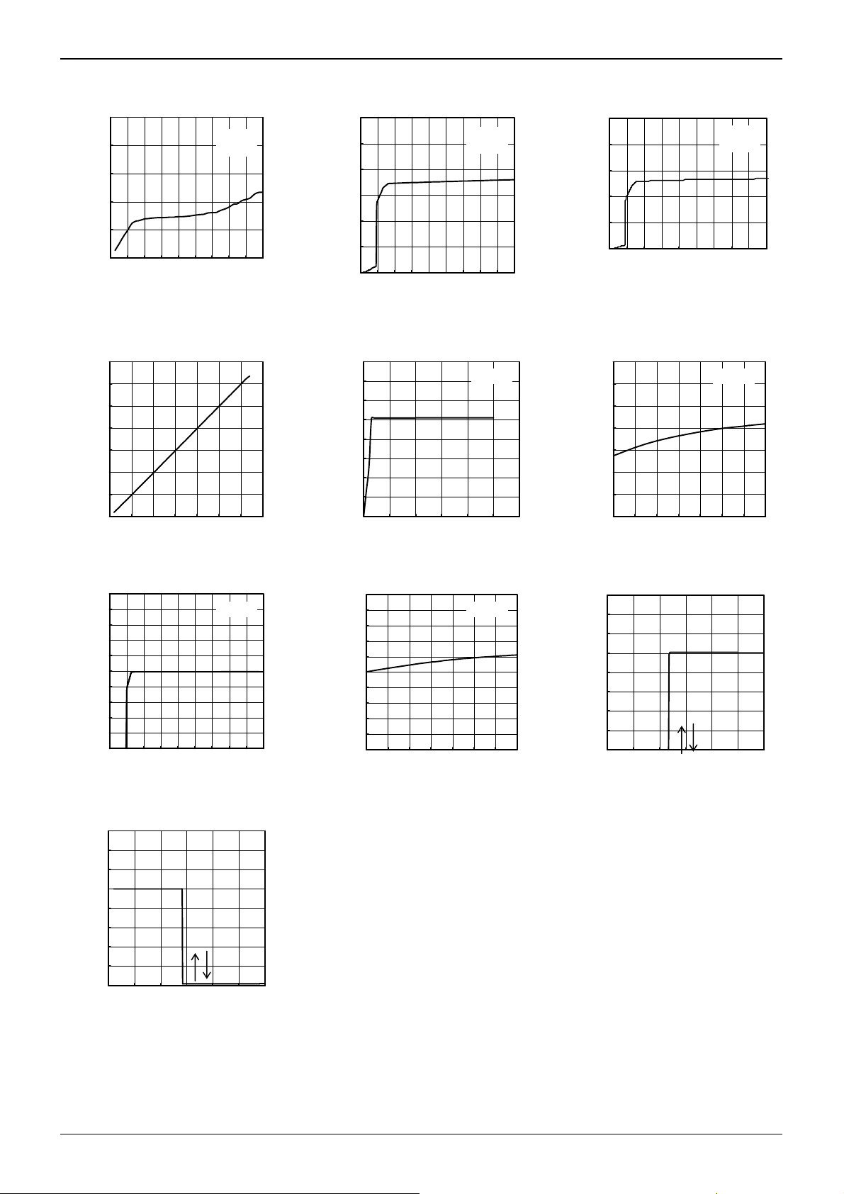
●Reference data(Unless specified,VCC=24V, Ta=25℃)
0.05
0.04
0.03
0.02
ICC [mA]
0.01
0.00
0 4 8 12162024283236
STBY=L
EN=L
VCC [V]
Fig..4-1 Circuit electric current
(at the time of OFF mode)
35
30
25
20
15
ILED [mA]
10
5
0
0 0.5 1 1.5 2 2.5 3 3.5
VSET [V]
Fig..4-4 VSET Constant electric
current Characteristics
10
9
8
7
6
5
4
VREG [V]
3
2
1
0
0 4 812162024283236
VCC [V]
Io=0mA
Fig..4-7 VREG_VCC characteristic
8
7
6
5
4
3
VRED [V]
2
1
0
0 0.5 1 1.5 2 2.5 3
VEN [V]
Fig..4-10 EN Threshold voltage
3.0
2.5
2.0
1.5
ICC [mA]
1.0
0.5
0.0
0 4 8 12 162024283236
Fig..4-2 Circuit electric current
at the time of stand bymode
32
28
24
20
16
12
ILED [mA]
8
4
0
0123456
Fig..4-5 VLED Dependency of ILED
5.5
5.4
5.3
5.2
5.1
5.0
4.9
VREG [V]
4.8
4.7
4.6
4.5
-40 -20 0 20 40 60 80 100
Fig..4-8 VREG temperature
VCC [V]
VSET [V]
TEMP [℃]
characteristic
Technical Note
5
STBY=H
EN=L
VSET=2V VSET=2V
Io=0mA
4
3
2
ICC [mA]
1
0
0 4 8 12162024283236
VCC [V ]
Fig..4-3 Circuit electric current
at the time of operatingmode
24
23
22
21
20
ILED [mA]
19
18
17
-40 -20 0 20 40 60 80 100
TEMP [℃]
Fig..4-6 Constant electric current
temperature characteristic
8
7
6
5
4
3
VREG [V]
2
1
0
0 0.5 1 1.5 2 2.5 3
VSTBY [V]
Fig..4-9 STBY Threshold voltage
STBY=H
EN=H
www.rohm.com
4/12
© 2009 ROHM Co., Ltd. All rights reserved.
2009.07 - Rev.A

BD9206EFV
p
Technical Note
● Block functional descriptions
■PREREG, REF, 5VREG
PREREG is an circuit of constant voltage supplied to REF and 5VREG in which the voltage applied to VCC terminal is made
to be constant.
REF is a temperature-compensated reference voltage resource and used as reference voltage of TSD (Thermal Shutdown
Circuit).
5VREG is a 5V constant-voltage source and used as a power supply of constant-current driver.
The 5V constant voltage is output to VREG terminal. Moreover, it is recommended to attach a 1μF ceramic capacitor using
for phase correction, to VREG terminal.
■UVLO(Under Voltage Lock Out)
The LED driver is turned OFF when the VREG voltage is less than 2.9V(typ). The operation of lighting up is reset when
VREG becomes more than 3.0V(typ).
■ TSD(Thermal Shutdown Circuit)
TSD circuit protects the IC from thermo runaway or thermal damage.
TSD circuit detects the chip temperature and turns the circuit off if the chip temperature reaches 175℃. The hysteresis of
20℃ is set for TSD detection and release so as to prevent malfunction caused by temperature fluctuations.
■Current Driver(Constant-current driver), Driver Current Setting
Current Driver(Constant-current driver) is an circuit that generates a constant current for lighting of LED.
Constant-current circuit of BD9206EFV consists of the constant current setting part and the constant current driver part.
The constant-current driver part operates in such a manner that the voltage of Point a is equal to the voltage of point b
because the part serves as a buffer, the input of which is the voltage VX that is set by the constant current setting part.
Therefore, the current ILED that flows into the VLED terminal is as follows:
ILED = Vb/RSET = Va/RSET = VX/RSET = VSET*A/RSET = VSET*B
(A and B are numerical constants)
For BD9206EFV, the numerical constants inside the IC are set in such a way that the following formula is brought into
existence:
ILED(mA) = VSET *10 (VSET=0.6~3.0V)
If VSET is fixed, then the Vb is fixed, therefore the current ILED always flows independent of the fixed voltage of VLED.
However, the constant current operation is stopped if the voltage of VLED terminal is less than 0.6V, so please ensure
VLED>0.6V.
Vo
[Constant current driver part]
VSET
【定電流設定部】
[Constant current setting part]
VX=VSET*A
電圧
Voltage
shift circuit
変換
回路
VX
【定電流ドライバ部】
Condenser for phase
位相補償 用コンデンサ
com
ensation
a
+
-
EN
RSET
ILE D
VLED
b
Fig..5
www.rohm.com
5/12
© 2009 ROHM Co., Ltd. All rights reserved.
2009.07 - Rev.A

BD9206EFV
● Rise time and Fall time of LED Driver’s constant current
In the state of STBY=H, the rise time of constant current at the time of EN=L→H and the fall time at the time of EN=H→L
are as shown in the following table.
As shown in Fig.5, the constant current driver is formed in such a way that the NMOS of the driver output is made to be
operated or stopped by the EN signal.
Therefore, the rise time for the second time or later is shorter than the one for the first time because the electrical ch arge
of the capacitor for phase compensation is reopened from the charged state.
First time Second time or later Remarks
The time interval between the
Rise time 2.9μs ± 7% 2.6μs ± 7%
Fall time 0.7μs ± 11% 0.7μs ± 11%
On the condition that VCC=Vo=24V, VF(LED)=3.2V 5-stage connection, RL=15Ω
■STBY, EN
At the time of STBY=L, it becomes the OFF mode, then only a portion of the circuit inside the IC is operating, so the circuit
current is restricted to 17μA (typ).
At the time of STBY=H, it becomes the Standby mode, then 5VREG is started and UVLO is released before the LED driver
gets into the state of Ready.
After that, if EN=L→H, then the current flows into the LED driver and the LED is lighted up.
Note: If STBY and EN are simultaneously made to be L→H, then the rising edge of the LED driver gets late because t he
starting time of 5VREG is necessary.
If it is used after PWM dimming, then please let STBY=H beforehand and input the CLK to EN before using.
●Operation logic of LED driver
●Logic of LED driver protection circuit
EN
STBY
L Stop Stop
H Stop Operation
L H
STBY
UVLO
TSD
moment of EN=L→H and the
moment at which the I
reaches 90% of the set value
The time interval between the
moment of EN=H→L and the
moment at which the I
reaches 10% of the set value
EN
active : High
Technical Note
LED
LED
LED
Driver
Function Stop Operation
UVLO VREG < 2.9V(typ) VREG > 3.0V(typ)
TSD Ta > 175℃ Ta < 155℃
■TEST terminal
TEST terminal is only used in ROHM’s testing process before delivery, so please use the IC with the terminal fixed at Low in
normal times.
www.rohm.com
6/12
© 2009 ROHM Co., Ltd. All rights reserved.
2009.07 - Rev.A
BD9206EFV
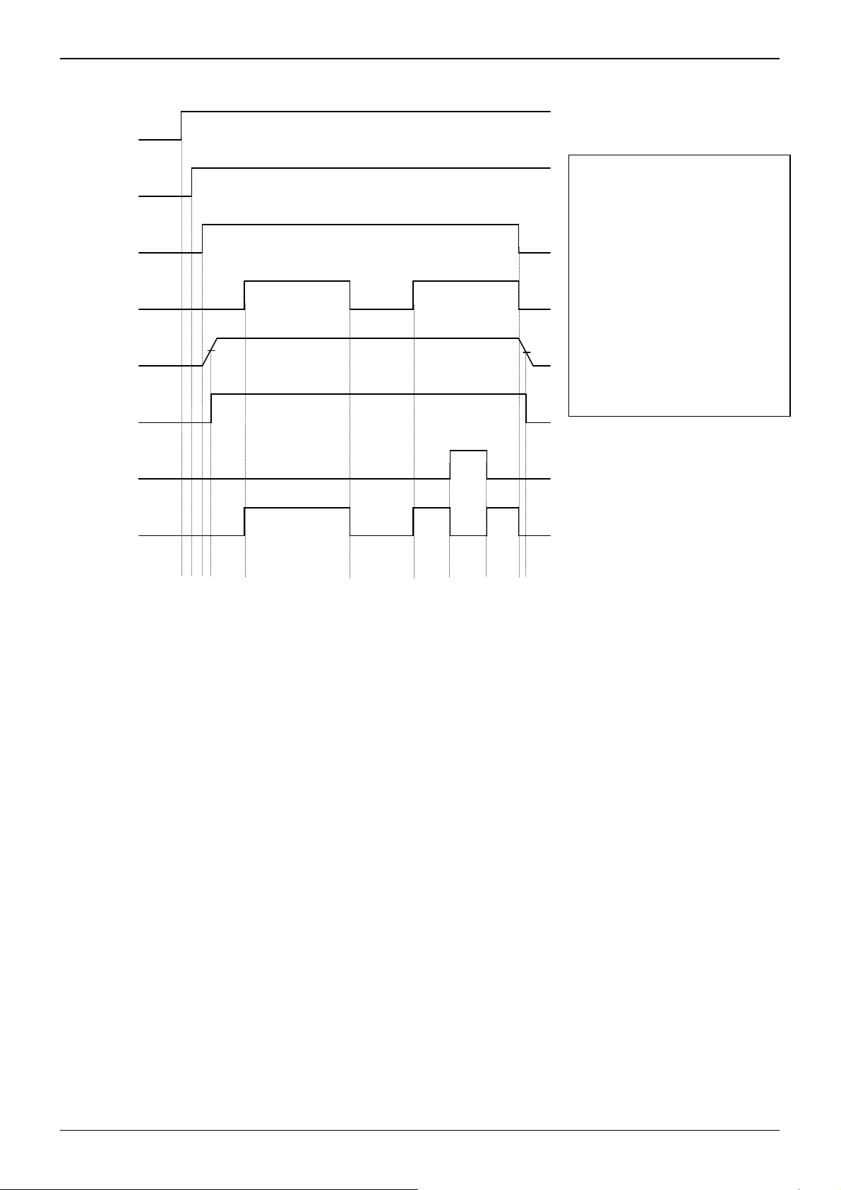
●Timing chart
VCC
VSET
STBY
EN
VREG
UVLO internal signal
UVLO( 内部信号)
TSD internal signal
TSD(内部信号)
I
LED
※Please be careful about a current flowing to the VCC side via the diode for electrostatic breakdown protection if a
voltage is applied to STBY terminal or EN terminal earlier than to VCC terminal.
3.0V
①②③④ ⑤ ⑥ ⑦ ⑧ ⑨ ⑩⑪
Fig..7
2.9V
Technical Note
① VCC input.
② VSET Setting
③ It moves to OFF mode due to STBY =
L -> H. 5VREG (VREG) start. Rising
time ms.
④ It becomes UVLO = H depending upon
VREG >3.0V, it moves to stand-by
mode. As for LED driver, it is ready
state.
⑤ LED Lighting with EN = L -> H .
⑥ LED lighting out with EN = H → L
⑦ it is same with ⑤
⑧ Detecting TSD with Ta > 175℃,
LED lighting out
⑨ Deleting TSD with Ta < 155℃,
LED lighting
⑩LED lighting out with STBY,EN=H→L
⑪Detecting UVLO=L with VREG<2.9V
www.rohm.com
7/12
© 2009 ROHM Co., Ltd. All rights reserved.
2009.07 - Rev.A
BD9206EFV
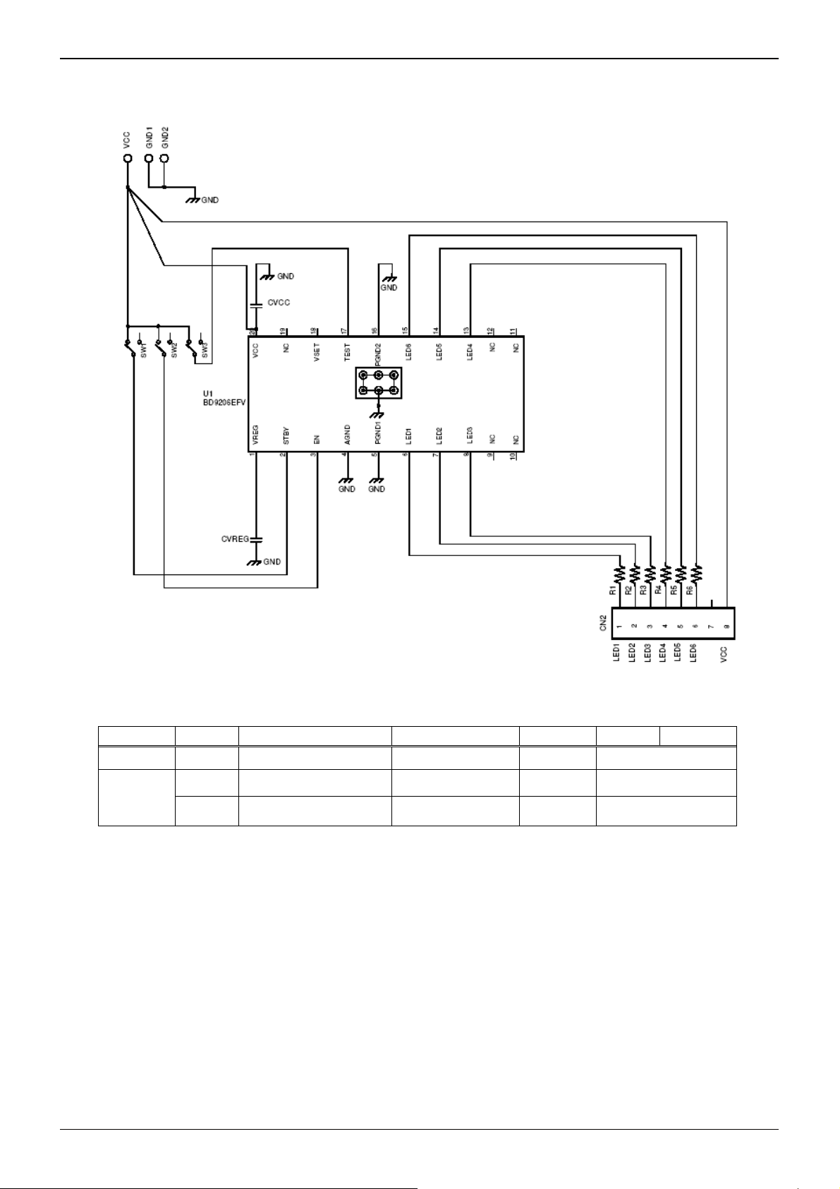
●Recommendation of Circuit figure
When you use VCC=24V ILED=20mA
Variety Symbol Usage Type Maker Value Unit
Resistance R1~R6 For reducing IC thermal loss MCR03Series15R0 ROHM 15Ω
Technical Note
Fig..8
capacitor
CVCC For input by-pass capacitor GMR55DB31H106 murata 10uF
CVREG For VREG phase compensation GMR188R71A105 murata 1uF
●The points of manufacturing substrate
For this IC, at the time of LED lighting, the temperature of the package increases due to heat generation of the constant
current driver.
Therefore, please bring the radiating fin on the back side of the package down to the GND with wide substrate pattern in
order to promote heat radiation.
In addition, the heat radiation can be further promoted by putting a thermal VIA in.
The heat radiation can be promoted similarly by connecting the unconnected terminals, TEST terminals and unused
terminals of LED1~6 to GND.
www.rohm.com
8/12
© 2009 ROHM Co., Ltd. All rights reserved.
2009.07 - Rev.A

BD9206EFV
Technical Note
●The calculation of electric power consumption for IC and the deciding method of external resistance value
Electric power consumption of IC is decided with formula below.
P(N)=ICC*VCC+[(Vo-RL*ILED)-(Vf+⊿Vf+⊿VfT)*M]*N*ILED ・・・・①
ICC
VCC
Vf
⊿Vf
⊿VfT
M
N
ILED
Vo
IC Consumed electric
:
current
:
Input voltage
:
LED Vf voltage
:
(normal temperature typ)
:
LED Vf Variation
:
LED Vf Temperature
:
variation
Stage number around
:
LED 1 line
:
LED line number
:
LED Constant current
value
Voltage OF LED anode
Vo
RL
VF
*M
*N
ILED
side
RL
external resistance
(external loss)
Fig..9
Please insert the heat-radiation resistor RL in order to decrease the heat radiation at the IC.
If the value of RL is made to be larger, then the heat radiation of the IC is decreased, but if the terminal voltage VLED of the
LED driver is less than 0.6V, then the constant current operation becomes impossible, therefore please set the RL in such a way
that the following expression is met:
VLED=Vo-(Vf+⊿Vf+⊿VfT)*M-RL*ILED>0.6V
Please set the ILED and RL in such a way that the relational expressions ① & ② are met.
Moreover, the permissible loss of the package is as shown in the following graph.
HTSSOP-B20 Pd
4.0
3.5
3.0
2.5
2.0
1.5
許容損失Pd(W)
allowable loss
1.0
3.20
2.30
1.00
③
②
①1layer baseplate
①:1層基板
Heat dissipation
(
(表層放熱銅箔:
copper foil on surface
Omm2)
0mm2
②2layer base―plate
Heat dissipation
(
copper foil on Inside
②:2層基板
and outside layer:
(表裏層放熱銅箔:
4900mm2)
4900mm2)
:
①
0.5
0.0
0 25 50 75 100 125 150
Temperature around Ta(℃)
周囲温度Ta(℃)
③4layer base―plate
③:4層基板
(
Heat dissipation
(全層放熱銅箔:
copper foil on whole
layer:4900mm2)
4900mm2
Fig..10
www.rohm.com
9/12
© 2009 ROHM Co., Ltd. All rights reserved.
2009.07 - Rev.A
BD9206EFV
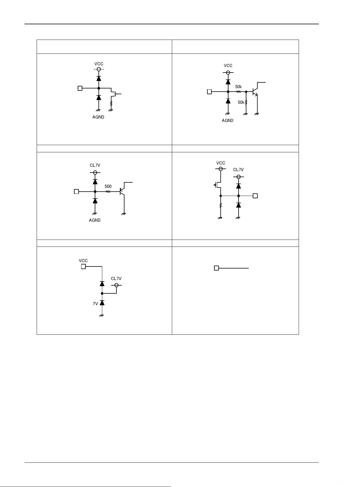
●Input/output equivalent circuit
6:LED1, 7:LED2, 8:LED3,
13:LED4, 14:LED5, 15:LED6
18:VSET 1:VREG
Technical Note
2:STBY
3:EN, 17:TEST
CL7V 9, 10, 11, 12, 19:N.C.
※The voltage clamp element of 7V is connected to CL7V.
N.C. pin is not connected
www.rohm.com
10/12
© 2009 ROHM Co., Ltd. All rights reserved.
2009.07 - Rev.A

BD9206EFV
子
Technical Note
●Notes for use
1.) The absolute maximum ratings
We pay sufficient attention for quality control to this product but If the absolute maximum ratings are exceeded, such as with
applied voltage or operational temperature range, a degradation or a destruction may occur. The short or open modes cannot be
specified. so if special modes which exceed the absolute maximum ratings are assumed, physical safety precautions such as fuses
should be in place.
2.) Reverse connection of power supply connector
The reverse connection of power connector may cause damage to IC. Please take countermeasures such as inserting a
diode between the power supply and IC’s external power supply pin for protection against the damage caused by the
reverse connection.
3.) Power supply line
The return of the regenerated current is caused by the back electromotive force of the external co il, so please take the
measures such as inserting a capacitor between power supply and GND as a route of r egenerated current, and determine
the capacitance value after thoroughly ensuring that there is no proble ms in the Characteristics of electrolyte capacitor,
such as no loss of capacitance at low temperature. Heat design should take into account of power dissipation (Pd) under actual
usage conditions, with wide enough margins
4.) GND Potential
The potential of the GND terminal should be the minimum potential under all operating conditions.
5.) Heat Design
Heat design should take into account of power dissipation under actual usage conditions, with wide enough margins.
6.) Short-circuiting between Terminals and Incorrect Mounting
When mounting to the PWB, pay special attention to the direction and proper placement of the IC. If the IC is attached incorrectly,
it may be destroyed. Furthermore, there is also a possibility of breakdown, when the foreign body enters during outputting and
between power supply and GND.
7.) The operation in the strong magnetic fields
Please be careful that there is a possibility of malfunction which is happening when you use it in a strong electrom agnetic
field.
8.) ASO
Please do the setting in such a way that the output Tr does not exceed the absolute maximum rating and ASO in case of
using this IC. For CMOS IC and the IC with more than one power supply, a rush current may flow instantaneously at the
time of power on, so please be careful about power supply coupling capacitance, power supply, GND pattern wiring width
and length.
9.) Thermal shutdown circuit (TSD circuit)
This IC incorporates a built-in thermal shutdown circuit (TSD circuit). The TSD circuit is that has des igned only to shut the
IC off to prevent the thermal runaway operation,not for IC protection or guarantee as purpose. Therefore, please do not
continue to use the IC after operating this circuit and also do not use the IC designating operation as prerequisite.
10.) Inspection of the Set Substrate
If a condenser is connected to a pin with low impedance when inspecting the set substrate , stress ma y be placed on the IC,
so please be sure to discharge after each process. Moreover, please be sure to turn off the power supply before connecting
& inspecting or before detaching when it is connected to jig at inspection process.
11.) About IC terminal input
This IC is a monolithic IC, and there are a P+ isolation and the P substrate for separation of element between each element. There is
a P-N junction formed between this P-layer and each element’s N-layer, forming every parasitic element, as shown in Fig.15, when
resistance and transistor are connected with terminal
〇 In the case of GND>(terminal A
ith resistance or GND>(terminal B) with transistor(NPN), the P-N junction operates as a
)w
parasitic diode.
〇 In addition, when GND> (terminal B) with the transistor (NPN), the parasitic NPN transistor operates due to the aforementioned
parasitic diode and the N layer of the other element approached
With the IC’s configuration, the production of parasitic elements is inevitable. The operation of parasitic elements causes
interferences between circuits, leading to malfunction and even destruction. Therefore, uses which cause the parasitic elements
to operate, such as applying voltage to the input terminal which is lower than the GND (P-substrate), should be avoided.
Resistance
+
抵抗
N
P Substrate
基板
P
P
Parasitic Element
寄生素子
GND
~ ~
(terminalB)
(端子B)
+
P
N
N
Parasitic Element
(terminalA)
(端子A)
P
N
P
C
(NPN)
+
寄生素子
Transistor
トランジスタ
B
N
N
P Substrate
基板
P
~ ~
P
GND
E
(terminalA)
GND
+
P
N
(端子A)
GND
~
~
Parasitic Element
寄生素子
other element approached
近接する他の素子
(terminalB)
(端子B)
C
B
~ ~
E
GND
Parasitic Element
寄生素
Fig..11 バイポーラ IC の簡易構造例
Fig.11 Simple Structure of bipolar IC (Sample)
www.rohm.com
11/12
© 2009 ROHM Co., Ltd. All rights reserved.
2009.07 - Rev.A

BD9206EFV
●Ordering part number
B D 9 2 0 6 E F V - E 2
Part No. Part No.
HTSSOP-B20
6.4±0.2
0.325
1.0MAX
0.85±0.05
6.5±0.1
(MAX 6.85 include BURR)
(4.0)
4.4±0.1
110
0.65
0.08±0.05
0.24
1120
1.0±0.2
+0.05
0.17
-
0.03
(Unit : mm)
0.5±0.15
+0.05
-
0.04
(2.4)
S
0.08 S
Package
EFV: HTSSOP-B20
<Tape and Reel information>
Embossed carrier tape (with dry pack)Tape
Quantity
Direction
of feed
2500pcs
E2
The direction is the 1pin of product is at the upper left when you hold
()
reel on the left hand and you pull out the tape on the right hand
Reel
Packaging and forming specification
E2: Embossed tape and reel
1pin
Order quantity needs to be multiple of the minimum quantity.
∗
Technical Note
Direction of feed
www.rohm.com
12/12
© 2009 ROHM Co., Ltd. All rights reserved.
2009.07 - Rev.A

Notes
No copying or reproduction of this document, in part or in whole, is permitted without the
consent of ROHM Co.,Ltd.
The content specied herein is subject to change for improvement without notice.
The content specied herein is for the purpose of introducing ROHM's products (hereinafter
"Products"). If you wish to use any such Product, please be sure to refer to the specications,
which can be obtained from ROHM upon request.
Examples of application circuits, circuit constants and any other information contained herein
illustrate the standard usage and operations of the Products. The peripheral conditions must
be taken into account when designing circuits for mass production.
Great care was taken in ensuring the accuracy of the information specied in this document.
However, should you incur any damage arising from any inaccuracy or misprint of such
information, ROHM shall bear no responsibility for such damage.
The technical information specied herein is intended only to show the typical functions of and
examples of application circuits for the Products. ROHM does not grant you, explicitly or
implicitly, any license to use or exercise intellectual property or other rights held by ROHM and
other par ties. ROHM shall bear no responsibility whatsoever for any dispute arising from the
use of such technical information.
Notice
The Products specied in this document are intended to be used with general-use electronic
equipment or devices (such as audio visual equipment, ofce-automation equipment, communication devices, electronic appliances and amusement devices).
The Products specied in this document are not designed to be radiation tolerant.
While ROHM always makes ef forts to enhance the quality and reliability of its Products, a
Product may fail or malfunction for a variety of reasons.
Please be sure to implement in your equipment using the Products safety measures to guard
against the possibility of physical injury, re or any other damage caused in the event of the
failure of any Product, such as derating, redundancy, re control and fail-safe designs. ROHM
shall bear no responsibility whatsoever for your use of any Product outside of the prescribed
scope or not in accordance with the instruction manual.
The Products are not designed or manufactured to be used with any equipment, device or
system which requires an extremely high level of reliability the failure or malfunction of which
may result in a direct threat to human life or create a risk of human injury (such as a medical
instrument, transportation equipment, aerospace machinery, nuclear-reactor controller,
fuel-controller or other safety device). ROHM shall bear no responsibility in any way for use of
any of the Products for the above special purposes. If a Product is intended to be used for any
such special purpose, please contact a ROHM sales representative before purchasing.
If you intend to export or ship overseas any Product or technology specied herein that may
be controlled under the Foreign Exchange and the Foreign Trade Law, you will be required to
obtain a license or permit under the Law.
Thank you for your accessing to ROHM product informations.
More detail product informations and catalogs are available, please contact us.
ROHM Customer Support System
www.rohm.com
© 2009 ROHM Co., Ltd. All rights reserved.
http://www.rohm.com/contact/
R0039
A
 Loading...