

Large Current External FET Controller Type Switching Regulator
Dual-output, high voltage,
high-efficiency step-down
Switching Regulator
(Controller type)
BD9011EKN , BD9011KV , BD9775FV
●Overview
The BD9011EKN/KV is a 2-ch synchronous controller with rectification switching for enhanced power management efficiency.
It supports a wide input range, enabling low power consumption ecodesign for an array of electronics.
●Features
1) Wide input voltage range: 3.9V to 30V
2) Precision voltage references: 0.8V±1%
3) FET direct drive
4) Rectification switching for increased efficiency
5) Variable frequency: 250k to 550kHz (external synchronization to 550kHz)
6) Built-in selected OFF latch and auto remove over current protection
7) Built-in independent power up/power down sequencing control
8) Make various application , step-down , step-up and step-up-down
9) Small footprint packages: HQFN36V, VQFP48C
●Applications
Car audio and navigation systems, CRTTV,LCDTV,PDPTV,STB,DVD,and PC systems,portable CD and DVD players,
etc.
●Absolute Maximum Ratings (Ta=25℃)
TECHNICAL NOTE
Parameter Symbol
EXTVCC Voltage EXTVCC 34 *1 V COMP1,2 Voltage COMP1,2
VCCCL1,2 Voltage VCCCL1,2 34 *1 V DET1,2 Voltage DET1,2
CL1,2 Voltage CL1,2 34 V RT、SYNC Voltage RT、SYNC
SW1,2 Voltage SW1,2 34 *1 V
BOOT1,2 Voltage BOOT1,2 40 *1 V
BOOT1,2-SW1,2
Voltage
STB, EN1,2 Voltage STB, EN1,2 VCC V
VREG5,5A
VREG33 VREG33 VREG5 V Storage temperature Tstg -55 to +150 ℃
SS1,2、FB1,2
*1 Regardless of the listed rating, do not exceed Pd in any circumstances.
*2 Mounted on a 70mm x 70mm x 0.8mm glass-epoxy board. De-rated at 7.44mW/℃(
above 25℃.
BOOT1,2-SW1,2 7
VREG5,5A 7 V
SS1,2、FB1,2
Rating Unit
*1
V
VREG5
V
Parameter Symbol
Power Dissipation
Operating
temperature
Junction temperature Tj +150 ℃
HQFN36V) or 8.8mW/℃(VQFP48C)
Pd
Topr
Rating Unit
VREG5 V
*2
0.875
(HQFN36V)
*2
1.1
(VQFP48C)
-40 to +105
W
W
℃
Apr.2008
●Operating conditions (Ta=25℃)
Parameter Symbol Min. Typ. Max. Unit
Input voltage 1 EXTVCC 3.9 *1 *2 12 30 V
Input voltage 2 VCC 3.9 *1 *2 12 30 V
BOOT-SW voltage BOOT-SW 4.5 5 VREG5 V
Carrier frequency OSC 250 300 550 kHz
Synchronous frequency SYNC OSC - 550 kHz
Synchronous pulse duty Duty 40 50 60 %
Min OFF pulse TMIN - 100 - nsec
★This product is not designed to provide resistance against radiation.
*1 After more than 4.5V, voltage range.
*2 In case of using less than 6V, Short to VCC, EXTVCC and VREG5.
●Electrical characteristics (Unless otherwise specified, Ta=25℃
VCC=12V STB=5V EN1,2=5V)
Parameter Symbol
Min. Typ. Max.
Unit Conditions
VIN bias current IIN - 5 10 mA
Shutdown mode current IST - 0 10 μA VSTB=0V
[Error Amp Block]
Limit
Feedback reference voltage
Feedback reference voltage
(Ta=-40 to 105℃)
VOB 0.792 0.800 0.808 V
VOB+ 0.784 0.800 0.816 V Ta=-40 to 105℃ ※
Open circuit voltage gain Averr - 46 - dB
VO input bias current IVo+ - - 1 μA
[FET Driver Block]
HG high side ON resistance
HG low side ON resistance
LG high side ON resistance
LG low side ON resistance
HGhon - 1.5 - Ω
HGlon - 1.0 - Ω
LGhon - 1.5 - Ω
LGlon - 0.5 - Ω
[Oscillator]
Carrier frequency FOSC 270 300 330 kHz RT=100 kΩ
Synchronous frequency Fsync - 500 - kHz RT=100 kΩ,SYNC=500kHz
[Over Current Protection Block]
CL threshold voltage
CL threshold voltage
(Ta=-40 to 105℃)
Vswth 70 90 110 mV
Vswth+ 67 90 113 mV Ta=-40 to 105℃ ※
[VREG Block]
VREG5 output voltage VREG5 4.8 5 5.2 V IREF=6mA
VREG33 reference voltage VREG33 3.0 3.3 3.6 V IREG=6mA
VREG5 threshold voltage VREG_UVLO 2.6 2.8 3.0 V VREG:Sweep down
VREG5 hysteresis voltage DVREG_UVLO 50 100 200 mV VREG:Sweep up
[Soft start block]
Charge current
Charge current
(Ta=-40 to 105℃)
ISS 6.5 10 13.5 μA VSS=1V
ISS+ 6 10 14 μA VSS=1V,Ta=-40 to 105℃ ※
Note: Not all shipped products are subject to outgoing inspection.
2/28
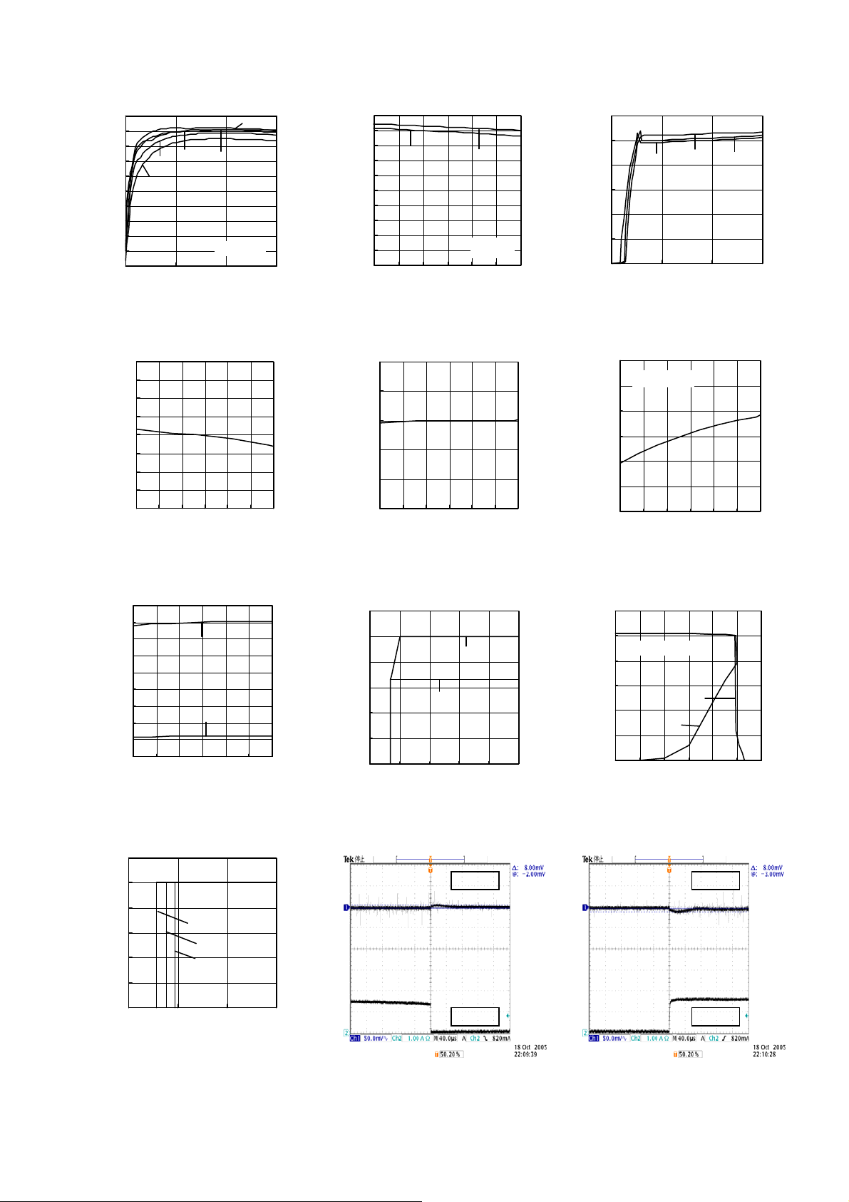
●Reference data (Unless otherwise specified, Ta=25℃)
p
p
]
L
100
90
80
70
60
50
40
EFFICIENCY[%]
30
20
10
0
0123
2.6V 3.3V
1.8V
1.2V
OUT PUT CURRE NT:Io[A]
5.0V
VIN=12V
Fig.1 Efficiency 1
0.816
0.812
0.808
0.804
0.800
0.796
0.792
0.788
RE FER ENC E VOL TAG E : VO B[V ]
0.784
-40 -15 10 35 60 85 110
AMBIENT TEMPERATURE : Ta[℃]
100
90
80
70
60
50
40
EFFICIENCY[%]
30
20
10
3.3V
0
6 9 12 15 18 21 24
INPUT VOLTAGE : V
Fig.2 Efficiency 2
110
100
90
80
70
過電流検出電圧 : Vswth[ mV]
60
-40 -15 10 35 60 85 110
AMBIENT TEMPERATURE : Ta[℃]
5.0V
Io=2A
[V]
IN
6
5
4
3
2
CIRC UIT CURRENT [mA]
1
0
0102030
INPUT VOLTAGE:V
105℃
25℃
-40℃
[V]
IN
Fig.3 Circuit current
330
RT=100kΩ
320
[kHz]
OSC
310
300
290
280
OSILATING FREQUENCY : F
270
-40 -15 10 35 60 85 110
AMBIENT TEMPERATURE : Ta[℃]
Fig.4 Reference voltage vs.
temperature characteristics
5.25
5.00
4.75
4.50
4.25
4.00
3.75
3.50
OUTPUT VOLTAGE : Vo [V]
3.25
3.00
-40 -15 10 35 60 85 110
VREG5
VREG33
AMBIENT TEMPERATURE : Ta[℃]
Fig.7 Internal Reg vs.
tem
erature characteristics
6
5
4
3
2
1
OUTPU T VOLTAGE : Vo[V]
0
0246
105℃
25℃
-40℃
INPUT VOLTAGE:V
[V]
EN
Fig.5 Over current detection vs.
temperature characteristics
6
5
3.3V
5.0V
[V]
IN
4
3
2
OUTPUT VOLTAGE : Vo [V]
1
0
0 5 10 15 20 25
INPUT VOLT AGE : V
OUTPUT VOLTAGE : Vo[V
Fig.6 Frequency vs.
tem
erature characteristics
3.0
2.5
RCL=15mΩ
2.0
1.5
1.0
0.5
0.0
LOFF=
0123456
OUTP UT CUR RENT: I o[A]
Fig.8 Line regulation Fig.9 Load regulation
50mV/div
VOUT VOUT
OUT
I
1A/div
I
OUT
LOFF= H
50mV/div
1A/div
Fig.10 EN threshold voltage Fig.11 Load transient response 1 Fig.12 Load transient response 2
3/28
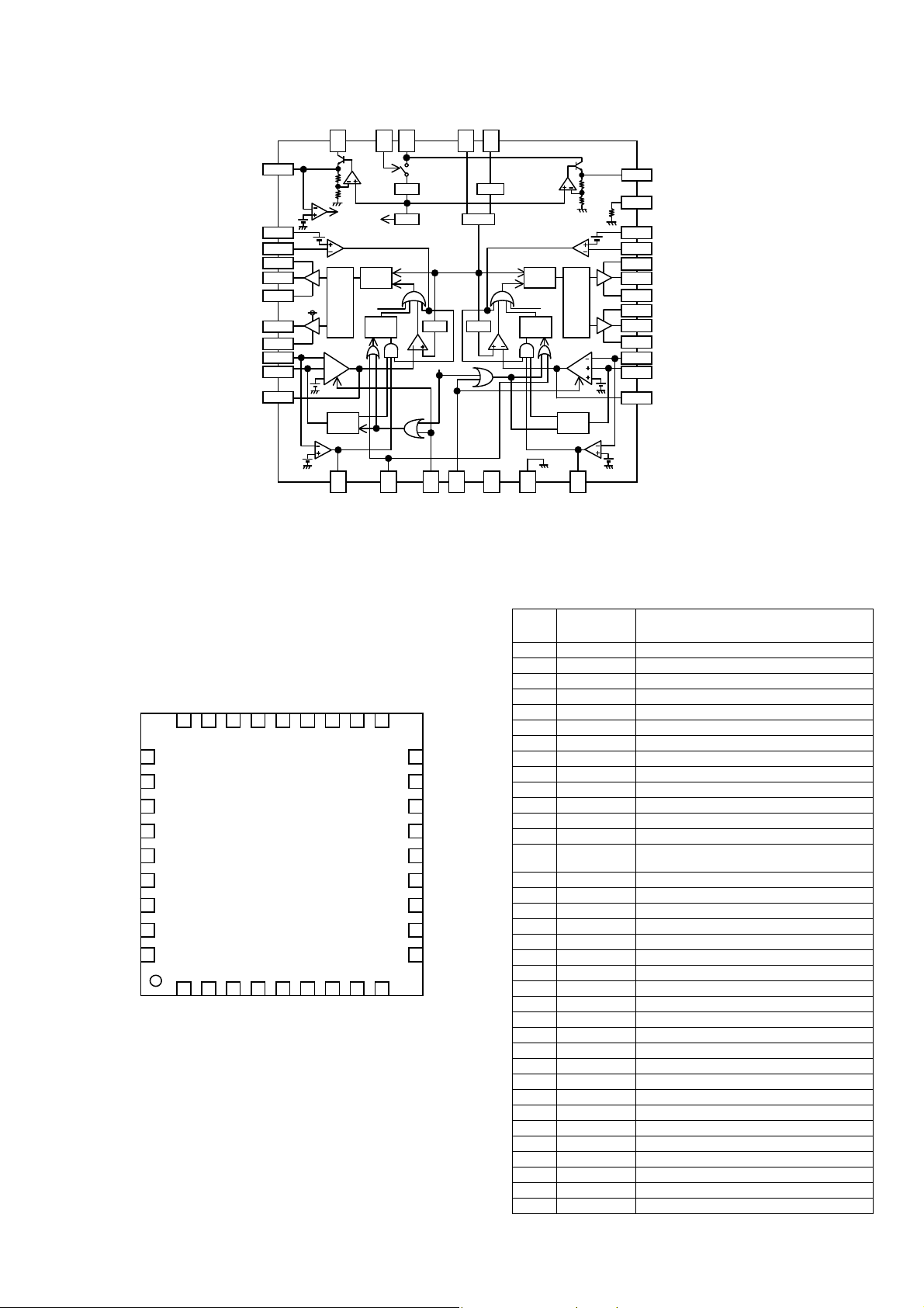
●Block diagram (Parentheses indicate VQFP48C pin numbers)
SYNC
OSC
Slope
(GNDS)
(34)
(30)
16
3.3V Reg
5(19)
17(35)
LLM
33(8)
VCCCL1
34(10)
35(11)
36(12)
1(13)
4(17)
3(15)
2(14)
6(21)
8(23)
7(22)
CL1
BOOT1
OUTH1
SW1
VREG5A
OUTL1
DGND1
FB1
SS1
COMP1
PWM
COMP
Set
Reset
Set
Sequence DET
13
(29)
GND
Q
Reset
DRV
TSD
UVLO
Err Amp
Q
Reset
OCP
SW
LOGIC
(24)
DET1
0.8V
Set
0.56V
9
24(44)
VREG5
CL2
BOOT2
OUTH2
SW2
OUTL2
DGND2
FB2
SS2
31(5)
30(3)
29(2)
28(1)
27(48)
25(46)
26(47)
21(39)
19(37)
20(38)
VCCCL2
COMP2
EXTVCC
22
(41) 10(25)
5V Reg
UVLO
2.7V
OCP
SW
VREG5
LOGIC
Err Amp
-
+
+
0.8V
Set
Reset
Sequence DET
0.56V
18
(36)
DET2 LOFF EN2 EN1
VCC RT
STB
32
(7)
B.G SYNC
TSD
TSD
Set
DRV
Reset
TSD
UVLO
Q
PWM
COMP
Reset Set
Q
14
(31)
Slope
UVLO
12
(27)
(26)
15
(33)
11
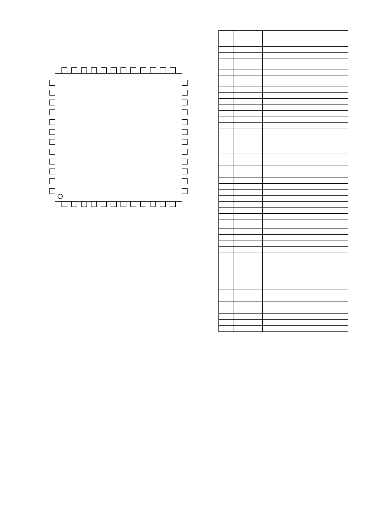
●Pin configuration
●PIN function table
BD9011EKN(HQFN36V)
SW2
DGND2
OUTL2
27 26 25 24 23 22 21 20 19
CL2
VCC
CL1
28
29
30
31
32
33
34
35
36
1 2 3 4 5 6 7 8 9
OUTH2
BOOT2
VCCCL2
VCCCL1
BOOT1
OUTH1
SW1
OUTL1
DGND1
VREG5
VREG33
VREG5A
Fig-14
EXTVCC
FB2
FB1
COMP1
COMP2
SS1
SS2
DET1
18
17
16
15
14
13
12
11
10
Fig-13
DET2
LMM
SYNC
RT
LOFF
GND
EN2
EN1
STB
Pin
Pin name Function
No.
1 SW1 High side FET source pin 1
2 DGND1 Low side FET source pin 1
3 OUTL1 Low side FET gate drive pin 1
4 VREG5A FET drive REG input
5 VREG33 Reference input REG output
6 FB1 Error amp input 1
7 COMP1 Error amp output 1
8 SS1 Soft start setting pin 1
9 DET1 FB detector output 1
10 STB Standby ON/OFF pin
11 EN1 Output 1ON/OFF pin
12 EN2 Output 2ON/OFFpin
13 GND Ground
14 LOFF
Over current protection OFF latch
function ON/OFF pin
15 RT Switching frequency setting pin
16 SYNC External synchronous pulse input pin
17 LLM Built-in pull-down resistor pin
18 DET2 FB detector output 2
19 SS2 Soft start setting pin 2
20 COMP2 Error amp output 2
21 FB2 Error amp input 2
22 EXTVCC External power input pin
23 - N.C.
24 VREG5 FET drive REG output
25 OUTL2 Low side FET gate drive pin 2
26 DGND2 Low side FET source pin 2
27 SW2 High side FET source pin 2
28 OUTH2 Hi side FET gate drive pin 2
29 BOOT2 OUTH2 driver power pin
30 CL2 Over current detector setting pin 2
31 VCCCL2 Over current detection VCC2
32 VCC Input power pin
33 VCCCL1 Over current detection VCC1
34 CL1 Over current detector setting pin 1
35 BOOT1 OUTH1 driver power pin
36 OUTH1 High side FET gate drive pin 1
4/28
●Pin configuration ●Pin function table
BD9011KV(VQFP48C)
DET2
36 35
LLM
34 33
SYNC
RT
32
LOFF
GNDS
GND
N.C
EN2
EN1
N.C
31
30 29
27 26 25
28
STB
BOOT1
24
DET1
23
SS1
22
COMP1
21
FB1
20
N.C
19
VREG33
18
N.C
17
VREG5A
16
N.C
15
OUTL1
14
DGND1
13
SW1
OUTH1
SS2
COMP2
FB2
N.C
EXTVCC
N.C
N.C
VREG5
N.C
OUTL2
DGND2
SW2
37
38
39
40
41
42
43
44
45
46
47
48
1 2
OUTH2
BOOT2
3 4
CL2
N.C
6
5
VCCCL2
8 9 10 11 12
7
N.C
VCC
VCCCL1
N.C
CL1
Fig-15
●Block functional descriptions
・Error amp
The error amp compares output feedback voltage to the 0.8V reference voltage and provides the comparison result as COMP voltage, which is
used to determine the switching Duty. COMP voltage is limited to the SS voltage, since soft start at power up is based on SS pin voltage.
・Oscillator (OSC)
Oscillation frequency is determined by the switching frequency pin (RT) in this block. The frequency can be set between 250kHz and 550kHz.
・ SLOPE
The SLOPE block uses the clock produced by the oscillator to generate a triangular wave, and sends the wave to the PWM comparator.
・PWM COMP
The PWM comparator determines switching Duty by comparing the COMP voltage, output from the error amp, with the triangular wave from the
SLOPE block. Switching duty is limited to a percentage of the internal maximum duty, and thus cannot be 100% of the maximum.
・Reference voltage (5Vreg,33Vreg)
This block generates the internal reference voltages: 5V and 3.3V.
・External synchronization (SYNC)
Determines the switching frequency, based on the external pulse applied.
・Over current protection (OCP)
Over current protection is activated when the VCCCL-CL voltage reaches or exceeds 90mV. When over current protection is active, Duty is low,
and output voltage also decreases. When LOFF=L, the output voltage has fallen to 70% or below and output is latched OFF. The OFF latch
mode ends when the latch is set to STB, EN.
・Sequence control (Sequence DET)
Compares FB voltage with reference voltage (0.56V) and outputs the result as DET.
・Protection circuits (UVLO/TSD)
The UVLO lock out function is activated when VREG falls to about 2.8V, while TSD turns outputs OFF when the chip temperature reaches or
exceeds 150℃. Output is restored when temperature falls back below the threshold value.
Pin
Pin name Function
No.
1 OUTH2 High side FET gate drive pin 2
2 BOOT2 OUTH2 driver power pin
3 CL2 Over current detection pin 2
4 N.C Non-connect (unused) pin
5 VCCCL2 Over current detection VCC2
6 N.C Non-connect (unused) pin
7 VCC Input power pin
8 VCCCL1 Over current detection CC1
9 N.C Non-connect (unused) pin
10 CL1 Over current detection setting pin 1
11 BOOT1 OUTH1 driver power pin
12 OUTH1 High side FET gate drive pin 1
13 SW1 High side FET source pin 1
14 DGND1 Low side FET source pin 1
15 OUTL1 Low side FET gate drive pin 1
16 N.C Non-connect (unused) pin
17 VREG5A FET drive REG input
18 N.C Non-connect (unused) pin
19 VREG33 Reference input REG output
20 N.C Non-connect (unused) pin
21 FB1 Error amp input 1
22 COMP1 Error amp output 1
23 SS1 Soft start setting pin 1
24 DET1 FB detector output 1
25 STB Standby ON/OFF pin
26 EN1 Output 1 ON/OFF pin
27 EN2 Output 2 ON/OFF pin
28 N.C Non-connect (unused) pin
29 GND Ground
30 GNDS Sense ground
31 LOFF
32 N.C Non-connect (unused) pin
33 RT Switching frequency setting pin
34 SYNC External synchronous pulse input pin
35 LLM Built-in pull-down resistor pin
36 DET2 FB detector output 2
37 SS2 Soft start setting pin 2
38 COMP2 Error amp output 2
39 FB2 Error amp input 2
40 N.C Non-connect (unused) pin
41 EXTVCC External power input pin
42 N.C Non-connect (unused) pin
43 N.C Non-connect (unused) pin
44 VREG5 FET drive REG output
45 N.C Non-connect (unused) pin
46 OUTL2 Low side FET gate drive pin 2
47 DGND2 Low side FET source pin 2
48 SW2 High side FET source pin 2
Over current protection OFF latch
function ON/OFF pin
5/28
(
)
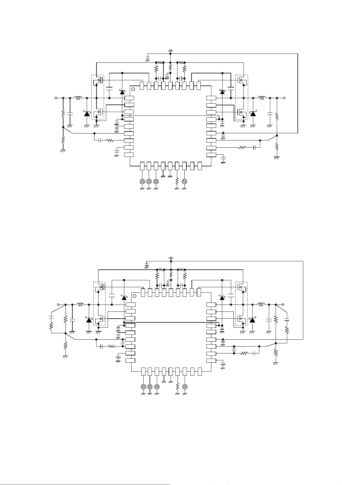
●Application circuit example (Parentheses indicate VQFP48C pin numbers)
Ω
BOOT1
EN1
15m
CL1
EN2
VIN(12V)
Ω
0.33
uF
33
(8)34(10)
VCCCL1
GND
15m
10
Ω
1nF1nF
31
32
(5)
(7)30(3)
VCC
VCCCL2
LOFF
RT
Ω
100
CL2
SYNC
Ω
29
(2)28(1)
BOOT2
DGND2
OUTL2
VREG5
EXTVCC
COMP2
DET2
LLM
SP8K2 SP8K2
100uF
100
1uF
1uF
39kΩ 15000pF
0.1uF
RB160
VA- 40
0.1
uF
(SLF12565:TDK)
68kΩ
10uH Vo(5V/3A)
RB051
L-40
220uF
(OSコン)
13kΩ
1(13)
2(14)
3(15)
4
5(19)
6(21)
7(22)
8(23)
9(24)
(17)
36
(12)35(11)
OUTH1
SW1
DGND1
OUTL1
VREG5A
VREG33
FB1
COMP1
SS1
DET1
STB
100kΩ
Fig-16A(Step-Down:Cout=OS Capacitor)
OUTH2
SW2
FB2
SS2
18
(36)17(35)16(34)15(33)14(31)13(29)12(27)11(26)10(25)
27(48)
26(47)
25(46)
24(44)
22(41)
21(39)
20(38)
19(37)
23
RB160
VA- 40
0.1
uF
1uF
0.33uF
39kΩ 15000pF
0.1uF
(SLF12565:TDK)
10uH Vo(3.3V/3A)
RB051
L-40
220uF
OS
47k
Ω
コン
15k
Ω
There are many factors(The PCB board layout, Output Current, etc.)that can affect the DCDC characteristics.
Please verify and confirm using practical applications.
VIN(12V)
3(15)
4(17)
5(19)
6(21)
7(22)
8(23)
9
1
2(14)
(24)
(13)
100uF
OUTH1
SW1
DGND1
OUTL1
VREG5A
VREG33
FB1
COMP1
SS1
DET1
3300pF
150
Ω
Vo(1 .8V/2 A)
15kΩ
12kΩ
(SLF10145:TDK)
10uH
RB051
L-40
30uF
(C2012JB
0J106K
TDK)
:
SP8K2 SP8K2
RB160
VA- 40
0.1
uF
1uF
1uF
330pF
1kΩ 10000pF
0.1uF
36
(12)35(11
STB
100
Ω
)
BOOT1
EN1
23m
34
(10)
CL1
EN2
12
(27)11(26)10(25)
23m
Ω
10
0.33
Ω
uF
1nF1nF
31
33
(5)
(8)32(7)30(3)
VCC
VCCCL1
VCCCL2
GND
LOFF
15
(33)14(31)13(29)
Ω
100
Ω
OUTH2
SW2
FB2
SS2
18
(36)17(35)
27
26(47)
25(46)
24
22(41)
21(39)
20(38)
19(37)
(48)
(44)
23
RB160
VA- 40
0.1
uF
1uF
0.33uF
330pF
0.1uF
(SLF10145:TDK)
10uH Vo(2.5V/2A)
RB051
L-40
30uF
(C2012JB
0J106K
TDK)
:
3.3kΩ 3300pF
43
1000pF
k
Ω
20k
510Ω
Ω
29
(2)28(1)
CL2
BOOT2
DGND2
OUTL2
VREG5
EXTVCC
COMP2
DET2
RT
SYNC
LLM
16
(34)
100kΩ
Fig-16B(Step-Down:Cout=Ceramic Capacitor)
There are many factors(The PCB board layout, Output Current, etc.)that can affect the DCDC characteristics.
Please verify and confirm using practical applications.
6/28
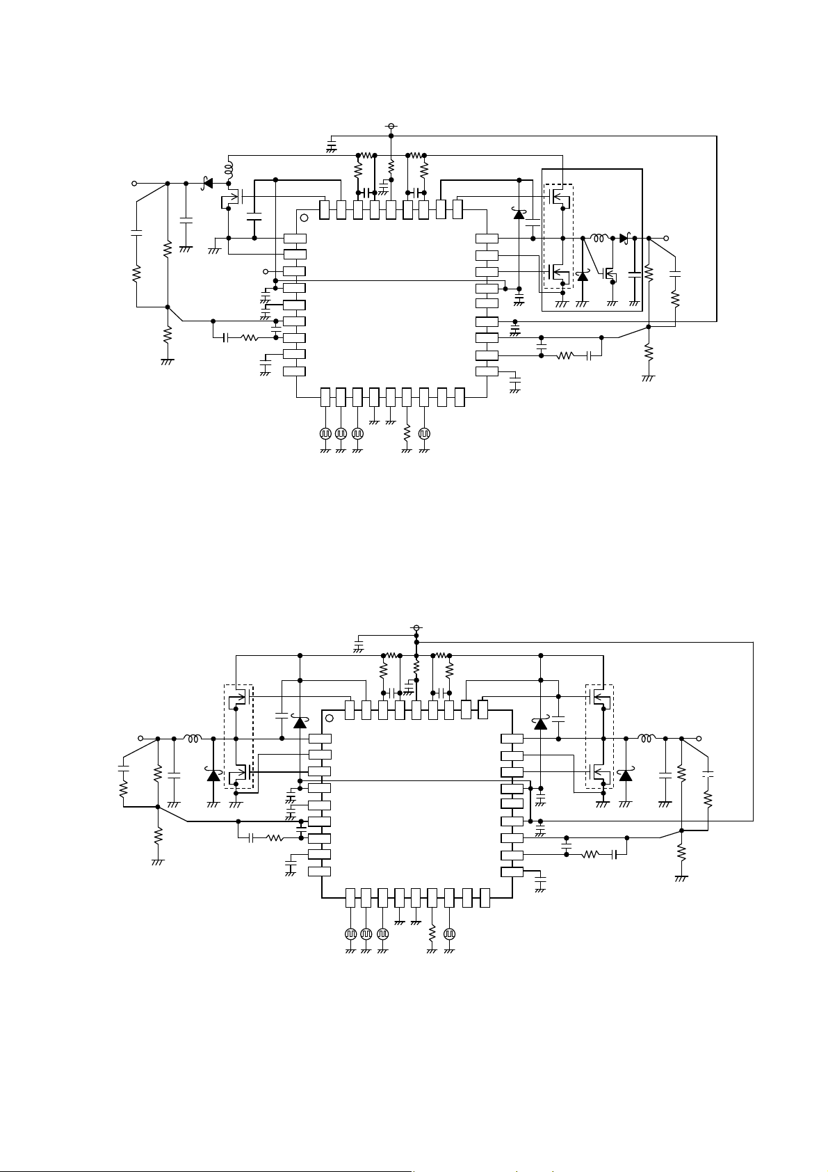
A
100
(11
35
Ω
(10)33(8)
)
BOOT1
EN1
12
(27)11(26)
10m
34
CL1
EN2
VIN(12V)
Ω
0.33
uF
VCCCL1
GND
100kΩ
10m
Ω
10
Ω
100
Ω
1nF1nF
OUTH2
SW2
OUTL2
FB2
SS2
18
(36)17(35)
27
26
25
24
22
21
20
19
RB160
VA- 40
(48)
(47)
(46)
(44)
23
(41)
(39)
(38)
(37)
0.1
uF
1000pF
1uF
0.33uF
0.1uF
32
(7)
VCC
29
30
(2)28(1)
(3)31(5)
CL2
BOOT2
VCCCL2
DGND2
VREG5
EXTVCC
COMP2
LOFF
15
(33)14(31)13(29)
DET2
RT
SYNC
LLM
16
(34)
*
SP8K2
(SLF12565:TDK)
4.7kΩ22000pF
REGSPIC
L2
27uH
RB051
L-40
Do3
Co2
220
uF
TM
Vo(12 V/1A)
91
kΩ
6.2kΩ
3300pF
10kΩ
* REGSPICTM is
Trade Mark of RHOM
Vo(2 4V/1A )
RB051L-40
L1
27uH
(SLF12565:TDK)
100uF
1
2
(15)
3
(17)
4
(19)
5
(21)
6
(22)
7
(23)
8
(24)
9
(13)
(14)
36
(12)
OUTH1
SW1
DGND1
OUTL1
VREG5A
VREG33
FB1
COMP1
SS1
DET1
STB
10
(25)
1000pF
5.1k
680
kΩ
Ω
23.5k
RSS
Co1
065N03
220uF
1uF
1uF
1uF
Ω
1000pF
10kΩ 22000pF
0.1uF
Fig-16C(Step-Down:Low Input Voltage)
There are many factors(The PCB board layout, Output Current, etc.)that can affect the DCDC characteristics.
Please verify and confirm using practical applications.
Vo(1.8V/2A)
3300pF
100
Ω
(SLF10145:TDK)
15kΩ
12kΩ
6.8uH
RB051
30uF
(
セラコン
L-40
VIN(5V)
100uF
SP8K2
RB160
-40
V
0.1uF
)
1uF
1uF
100pF
3.3kΩ 4700pF
0.1uF
1
2
3
4
5
6
7
8
9
(13)
(14)
(15)
(17)
(19)
(21)
(22)
(23)
(24)
OUTH1
SW1
DGND1
OUTL1
VREG5A
VREG33
FB1
COMP1
SS1
DET1
36
(12)35(11
STB
100
Ω
)
BOOT1
EN1
23m
34
(10)
CL1
EN2
12
(27)11(26)10(25)
23m
Ω
10
0.33
Ω
uF
1nF1nF
31
33
(5)
(8)32(7)30(3)
VCC
VCCCL1
VCCCL2
GND
LOFF
RT
15
(33)14(31)13(29)
Ω
16
(34)
100
CL2
SYNC
Ω
29
(2)28(1)
OUTH2
SW2
BOOT2
DGND2
OUTL2
VREG5
EXTVCC
COMP2
DET2
LLM
18
(36)17(35)
FB2
SS2
27
26
25
24
22
21
20
19
(48)
(47)
(46)
(44)
23
(41)
(39)
(38)
(37)
RB160
VA- 40
1uF
0.33uF
33pF
0.1uF
0.1uF
10kΩ 2200pF
SP8K2
(SLF10145:TDK)
6.8uH Vo(2.5V/2A)
RB051
L-40
30uF
(
)
セラコン
43
k
20k
1000pF
Ω
300Ω
Ω
100kΩ
Fig-16D(Step-Up:and Step-Up-Down)
There are many factors(The PCB board layout, Output Current, etc.)that can affect the DCDC characteristics.
Please verify and confirm using practical applications.
7/28
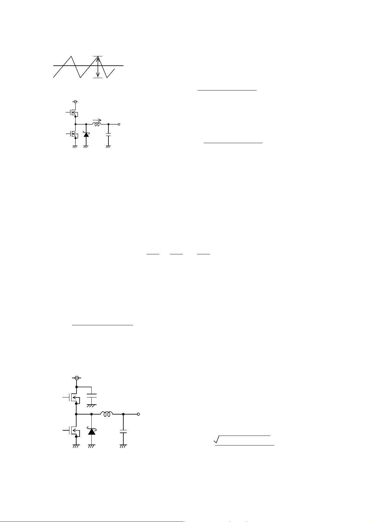
●Application component selection
(1) Setting the output L value
ΔIL
The coil value significantly influences the output ripple current.
Thus, as seen in equation (5), the larger the coil, and the higher
the switching frequency, the lower the drop in ripple current.
Fig-17
VCC
(VCC-VOUT)×VOUT
ΔIL = [A]・・・(5)
L×VCC×f
I
L
VOUT
The optimal output ripple current setting is 30% of maximum current.
ΔIL = 0.3×IOUTmax.[A]・・・(6)
L
Co
(VCC-VOUT)×VOUT
L = [H]・・・(7)
ΔIL×VCC×f
Fig-18
Output ripple current
(ΔIL:output ripple current f:switching frequency)
※Outputting a current in excess of the coil current rating will cause magnetic saturation of the coil and decrease
efficiency.
Please establish sufficient margin to ensure that peak current does not exceed the coil current rating.
※Use low resistance (DCR, ACR) coils to minimize coil loss and increase efficiency.
(2) Setting the output capacitor Co value
Select the output capacitor with the highest value for ripple voltage (V
PP) tolerance and maximum drop voltage
(at rapid load change). The following equation is used to determine the output ripple voltage.
ΔIL Vo 1
Step down ΔV
PP = ΔIL × RESR + × × [V] Note: f:switching frequency
Co Vcc
f
Be sure to keep the output Co setting within the allowable ripple voltage range.
※Please allow sufficient output voltage margin in establishing the capacitor rating. Note that low-ESR capacitors enable
lower output ripple voltage.
Also, to meet the requirement for setting the output startup time parameter within the soft start time range, please factor
in the conditions described in the capacitance equation (9) for output capacitors, below.
TSS × (Limit – IOUT) Tss: soft start time
Co ≦ ・・・ (9)
VOUT ILimit:over current detection value(2/16)reference
Note: less than optimal capacitance values may cause problems at startup.
(3) Input capacitor selection
VIN
The input capacitor serves to lower the output impedance of the power
source connected to the input pin (VCC). Increased power supply output
impedance can cause input voltage (VCC) instability, and may negatively
Cin
impact oscillation and ripple rejection characteristics. Therefore, be
certain to establish an input capacitor in close proximity to the VCC and
VOUT
L
Co
GND pins. Select a low-ESR capacitor with the required ripple current
capacity and the capability to withstand temperature changes without
wide tolerance fluctuations. The ripple current IRMSS is determined
using equation (10).
IRMS = IOUT × [A]・・・(10)
VOUT(VCC - VOUT)
Also, be certain to ascertain the operating temperature, load range and
Fig-19
Input capacitor
MOSFET conditions for the application in which the capacitor will be used,
since capacitor performance is heavily dependent on the application’s
input power characteristics, substrate wiring and MOSFET gate drain
capacity.
VCC
8/28
(4) Feedback resistor design
Please refer to the following equation in determining the proper feedback resistance. The recommended setting is in a range
between 10kΩ and 330kΩ. Resistance less than 10kΩ risks decreased power efficiency, while setting the resistance value
higher than 330kΩ will result in an internal error amp input bias current of 0.2uA increasing the offset voltage.
Internal ref. 0.8V
R8 +R9
Vo = × 0.8 [V] ・・・(11 )
R9
Fig-20
(5) Setting switching frequency
The triangular wave switching frequency can be set by connecting a resistor to the RT 15(33) pin. The RT sets the frequency
by adjusting the charge/discharge current in relation to the internal capacitor. Refer to the figure below in determining proper
RT resistance, noting that the recommended resistance setting is between 50kΩ and 130kΩ. Settings outside this range
may render the switching function inoperable, and proper operation of the controller overall cannot be guaranteed when
unsupported resistance values are used.
550
500
450
400
350
周波数 [ kHz ]
300
250
50 60 70 80 90 100 110 120 130
RT [ kΩ]
Fig-21 RT vs. switching frequency
(6) Setting the soft start delay
The soft start function is necessary to prevent an inrush of coil current and output voltage overshoot at startup. The figure
below shows the relation between soft start delay time and capacitance, which can be calculated using equation (12) at right.
0.8V(typ.)×CSS
TSS = [sec]・・・(12)
ISS(10μA Typ.)
10
1
0.1
DELAY TIME[ms]
0.01
0.001 0.01 0.1
SS CAPACITANCE[uF]
Fig-22 SS capacitance vs. delay time
Recommended capacitance values are between 0.01uF and 0.1uF. Capacitance lower than 0.01uF may generate output
overshoots. Please use high accuracy components (such as X5R) when implementing sequential startups involving other
power sources. Be sure to test the actual devices and applications to be used, since the soft start time varies, depending on
input voltage, output voltage and capacitance, coils and other characteristics.
9/28

A
(7) Setting over current detection values
V
The current limit value(ILimit)is determined by the resistance of the RCL established between CL and VCCCL.
VCCCL
CL
90m
ILimit = [A]・・・(13)
RCL
VIN
RCL
IL
L
I
L
Vo
Over current detection point
Fig-23 Fig-24
There are 2 current limit function (ON/OFF control type and OFF latch type) toggled by LOFF pin.
・LOFF=L (0<LOFF<1V): Off Latch Type Current Limit
The output becomes OFF and latched when SS=H and, current limit operation, and the output voltage is less than or equal
to 70% of Vo. The OFF latch is deactivated by re-inputting EN signal or VCC control input (switch OFF and ON once more).
・LOFF=H (1<LOFF<VREG5): ON/OFF Control Type Current Limit
When the current goes beyond the threshold value, the current can be limited by reducing the ON Duty Cycle. When the load
goes back to the normal operation, the output voltage also becomes back on to the specific
o
The current limit value
level.
LOFF=L
OFF Latch
(
)
Vo×70%
LOFF=H
Fig-25
Io
(8) Method for determining phase compensation
Conditions for application stability
Feedback stability conditions are as follows:
・When gain is 1 (0dB) and phase shift is 150° or less (i.e., phase margin is at least 30°):
a dual-output high-frequency step-down switching regulator is required
Additionally, in DC/DC applications, sampling is based on the switching frequency; therefore, overall GBW may be set at no
more than 1/10 the switching frequency. In summary, target characteristics for application stability are:
・Phase shift of 150° or less (i.e., phase margin of 30° or more) with gain of 1 (0dB)
・GBW (i.e., gain 0dB frequency) no more than 1/10 the switching frequency.
Stability conditions mandate a relatively higher switching frequency, in order to limit GBW enough to increase response.
The key to achieving successful stabilization using phase compensation is to cancel the secondary phase margin/delay
(-180°) generated by LC resonance, by employing a dual phase lead. In short, adding two phase leads stabilizes the
application.
GBW (the frequency at gain 1) is determined by the phase compensation capacitor connected to the error amp. Thus, a larger
capacitor will serve to lower GBW if desired.
① General use integrator (low-pass filter) ② Integrator open loop characteristics
Feedback
R
FB
COMP
C
Gain
[dB]
Phase
[deg]
18 0
90
0
-9 0
-90
-180
-180
A
0
0
(a)
-90°
Phase margin
-20dB/decade
GBW(b)
-180°
point (a) fa = 1.25[Hz]
point (b)点 fa = GBW [Hz]
1
2πRCA
1
2πRC
Fig-26 Fig-27
The error amp is provided with phase compensation similar to that depicted in figures ① and ② above and thus serves
as the system’s low-pass filter.
In DC/DC converter applications, R is established parallel to the feedback resistance.
10/28

A
A
When electrolytic or other high-ESR output capacitors are used:
A
Phase compensation is relatively simple for applications employing high-ESR output capacitors (on the order of several
Ω). In DC/DC converter applications, where LC resonance circuits are always incorporated, the phase margin at these
locations is -180°. However, wherever ESR is present, a 90° phase lead is generated, limiting the net phase margin to -90°
in the presence of ESR. Since the desired phase margin is in a range less than 150°, this is a highly advantageous
approach in terms of the phase margin. However, it also has the drawback of increasing output voltage ripple components.
③ LC resonance circuit ④ ESR connected
Vcc
Vcc
L
fr = [Hz]
Resonance point phase margin -180°
1
2π√LC
Vo
L
C
Fig-28 Fig-29
resonance point1
fr = [Hz]:Resonance Point
2π√LC
fESR = [Hz] :Zero
2πR
-90°:Pole
C
1
ESRC
Vo
ESR
R
Since ESR changes the phase characteristics, only one phase lead need be provided for high-ESR applications. Please choose
one of the following methods to add the phase lead.
⑤ Add C to feedback resistor ⑥ Add R3 to aggregator
Vo
R1
R2
Vo
R1
R2
FB
C2
COMP
C1
FB
R3
C2
COMP
Fig-30 Fig-31
Phase lead fz = [Hz] Phase lead fz = [Hz]
Set the phase lead frequency close to the LC resonance frequency in order to cancel the LC resonance.
1
2πC1R1
1
2πC2R3
When using ceramic, OS-CON, or other low-ESR capacitors for the output capacitor:
Where low-ESR (on the order of tens of mΩ) output capacitors are employed, a two phase-lead insertion scheme is
required, but this is different from the approach described in figure ③~⑥, since in this case the LC resonance gives rise
to a 180° phase margin/delay. Here, a phase compensation method such as that shown in figure ⑦ below can be
implemented.
⑦ Phase compensation provided by secondary (dual) phase lead
Vo
R1
R2
C1
R3
FB
COMP
C2
Phase lead fz1 = [Hz]
Phase lead fz2 = [Hz]
LC resonance frequency fr = [Hz]
1
2πR1C1
1
2πR3C2
1
2π√LC
Fig-32
Once the phase-lead frequency is determined, it should be set close to the LC resonance frequency.
This technique simplifies the phase topology of the DCDC Converter. Therefore, it might need a certain amount
of trial-and-error process. There are many factors(The PCB board layout, Output Current, etc.)that can affect
the DCDC characteristics. Please verify and confirm using practical applications.
11/ 28

f
f
A
A
(9)MOSFET selection
VCC
FET uses Nch MOS
DS>Vcc
・V
GSM1>BOOT-SW interval voltage
・V
GSM2>VREG5
・V
VGSM1
VDS
L
I
Vo
・Allowable current>voltage current + ripple current
※Should be at least the over current protection value
※Select a low ON-resistance MOSFET for highest efficiency
VGSM2
VDS
Fig-33
(10)Schottky barrier diode selection
VCC
・ Reverse voltage V
・ Allowable current>voltage current + ripple current
Vo
※Should be at least the over current protection value
※Select a low forward voltage, fast recovery diode for highest
efficiency
VR
・ The shoot-through may happen when the input parasitic
capacitance of FET is extremely big or the Duty ratio is less
than or equal to 10%. Less than or equal to 1000pF input
parasitic capacitance is recommended. Please confirm
Fig-34
operation on the actual application since this character is
affected by PCB layout and components.
(11)Sequence function
●Circuit diagram ●Timing chart
VCC VREG5
VREG5
Vo1
OUTH1 BOOT1 VCC BOOT2
SW1
OUTL1
DGND1
FB1
COMP1
SS1
DET2
STB EN1 EN2 GND
DGND2
COMP2
OUTH2
SW2
OUTL2
FB2
SS2
DET1
Fig-35 Fig-36
With EN1, 2 at ”H” level, when EN1 goes ”L” ,
Vo1 turns OFF, but Vo2 output continues.
EN1
EN2
Vo2
DET2
SS1
FB1
Vo1
DET1
SS2
FB2
Vo2
With EN1,2 at “H” level, i
Vo1 starts at 76% or more o
voltage setting, DET goes
open and SS1 is asserted,
starting Vo2 output.
R>Vcc
0.61V
over 76%
When EN1 stays ”H” and EN2 returns to ”H”, DET1 is in
open state; thus SS2 is asserted, and Vo2 output starts.
If Vo2 is 76% of the voltage setting or higher, DET2 goes
open and SS1 is asserted, starting Vo1 output.
0.61V
0.56V
under 70%
With EN2 set ”L”, if Vo2
goes below 70% the voltage
setting, DET2 shorts and SS1
is asserted, turning Vo1 OFF
over 76%
Same as “A” at left
0.56V
over 70%
12/28

●Input/Output equivalent circuits (Items in parentheses apply to VQFP48C)
/
1(13),27(48)PIN(SW1,SW2)
29(2),35(11)PIN(BOOT2,BOOT1)
28(1),36(15)PIN(OUTH1,OUTH2)
BOOT
2(14),26(47)PIN(DGND1,DGND2)
3(15),25(46)PIN(OUTL1,OUTL2)
24(44) VREG5 / 4(17)VREG5A
14(31)PIN(LOFF)
VREG5
OUTH
SW
300k
OUTL
DGND
16(34)PIN(SYNC) 6(21),21(39)PIN(FB1,FB2)
VREG5
250k
5k
1P
SYNC
10(25),11(26),12(27)PIN
(STB,EN1,EN2)
VCC
FB
VREG5
VREG5A
1k
2.5k
9(24),18(36)PIN(DET1,DET2) 15(33)PIN(RT)
VREG5
/ VREG5A
STB
EN
172.2k
135.8k
100k
DET
10k
LOFF
172.2k
100k
135.8k
8(23),19(37)PIN(SS1,SS2)
VREG5
/ VREG5A
SS
100k
VREG5
2k
50k
RT
17(35)PIN(LLM)
VREG5A
LLM
22(41)PIN(EXTV,CC)
24(44)PIN(VREG5)
EXTVCC
VCC
VREG5
VCC
308k
150k
746.32k
255k
30(3),34(10)PIN(CL2,CL1)
31(5),33(8)PIN(VCCCL2,VCCCL1)
VCCCL
CL
VCC
VCC
5P
1k
7(22),20(38)PIN(COMP1,COMP2)
VREG5
/ VREG5A
5k
COMP
20Ω
5kΩ
5kΩ
5(19)PIN(VREG33) 4(17)DIN(VREG5A)
VREG5A
VREG33
VCC
150k
746.32k
469.06k
VCC
VREG5A
13/28

●Operation notes
r
1)Absolute maximum ratings
Exceeding the absolute maximum ratings for supply voltage, operating temperature or other parameters can damage or
destroy the IC. When this occurs, it is impossible to identify the source of the damage as a short circuit, open circuit, etc.
Therefore, if any special mode is being considered with values expected to exceed absolute maximum ratings, consider
taking physical safety measures to protect the circuits, such as adding fuses.
2)GND electric potential
Keep the GND terminal potential at the lowest (minimum) potential under any operating condition.
3)Thermal design
Be sure that the thermal design allows sufficient margin for power dissipation (Pd) under actual operating conditions.
4)Inter-pin shorts and mounting errors
Use caution when positioning the IC for mounting on printed surface boards. Connection errors may result in damage or
destruction of the IC. The IC can also be damaged when foreign substances short output pins together, or cause shorts
between the power supply and GND.
5)Operation in strong electromagnetic fields
Use caution when operating in the presence of strong electromagnetic fields, as this may cause the IC to malfunction.
6)Testing on application boards
Connecting a capacitor to a low impedance pin for testing on an application board may subject the IC to stress. Be sure to
discharge the capacitors after every test process or step. Always turn the IC power supply off before connecting it to or
removing it from any of the apparatus used during the testing process. In addition, ground the IC during all steps in the
assembly process, and take similar antistatic precautions when transporting or storing the IC.
7) The output FET
The shoot-through may happen when the input parasitic capacitance of FET is extremely big or the Duty ratio is less than
or equal to 10%. Less than or equal to 1000pF input parasitic capacitance is recommended. Please confirm operation on
the actual application since this character is affected by PCB layout and components.
8)This monolithic IC contains P+ isolation and P substrate layers between adjacent elements in order to keep them isolated.
P-N junctions are formed at the intersection of these P layers with the N layers of other elements, creating a parasitic diode
or transistor. Relations between each potential may form as shown in the example below, where a resistor and transistor
are connected to a pin:
○ With the resistor, when GND> Pin A, and with the transistor (NPN), when GND>Pin B:
The P-N junction operates as a parasitic diode
○ With the transistor (NPN), when GND> Pin B:
The P-N junction operates as a parasitic transistor by interacting with the N layers of elements in proximity to the
parasitic diode described above.
Parasitic diodes inevitably occur in the structure of the IC. Their operation can result in mutual interference between circuits,
and can cause malfunctions, and, in turn, physical damage or destruction. Therefore, do not employ any of the methods
under which parasitic diodes can operate, such as applying a voltage to an input pin lower than the (P substrate) GND.
(PINA)
P
N
P
Resistor
(PINB)
+
P
N
P
Parasitic element
GND
+
N
Transistor(NPN)
C E
+
P
P
Parasitic element or transistor
B
P
N
P substrate
GND
+
N
(PINB)
C
B
E
GND
Parasitic element or transisto
(PINA)
Parasitic element
Fig-37 Fig-38 Fig-39 Fig-40
9)GND wiring pattern
When both a small-signal GND and high current GND are present, single-point grounding (at the set standard point) is
recommended, in order to separate the small-signal and high current patterns, and to be sure voltage changes stemming
from the wiring resistance and high current do not cause any voltage change in the small-signal GND. In the same way, care
must be taken to avoid wiring pattern fluctuations in any connected external component GND.
14/28

10)In some application and process testing, Vcc and pin potential may be reversed, possibly causing internal circuit or element
damage. For example, when the external capacitor is charged, the electric charge can cause a Vcc short circuit to the GND.
In order to avoid these problems, limiting output pin capacitance to 100μF or less and inserting a Vcc series countercurrent
prevention diode or bypass diode between the various pins and the Vcc is recommended.
Bypass diode
Fig-41
Countercurrent prevention diode
Vcc
Pin
11)Thermal shutdown (TSD)
This IC is provided with a built-in thermal shutdown (TSD) circuit, which is designed to prevent thermal damage to or
destruction of the IC. Normal operation should be within the power dissipation parameter, but if the IC should run beyond
allowable Pd for a continued period, junction temperature (Tj) will rise, thus activating the TSD circuit, and turning all output
pins OFF. When Tj again falls below the TSD threshold, circuits are automatically restored to normal operation. Note that
the TSD circuit is only asserted beyond the absolute maximum rating. Therefore, under no circumstances should the TSD
be used in set design or for any purpose other than protecting the IC against overheating
12)The SW pin
When the SW pin is connected in an application, its coil counter-electromotive force may give rise to a single electric
potential. When setting up the application, make sure that the SW pin never exceeds the absolute maximum value.
Connecting a resistor of several Ω will reduce the electric potential. (See Fig. 43)
BOOT
OUTH
SW
R
Fig-42
OUTL
DGND
Vcc
Vo
13)Dropout operation
When input voltage falls below approximately output voltage / 0.9 (varying depending on operating frequency) the ON
interval on the OUTL side MOS is lost, making boost applications and wrap operation impossible. If a small differential
between input and output voltage is envisioned for a prospective application, connect the load such that the SW voltage
drops to the GND level. Managing this load requires discharging the SW line capacitance (SW pin capacitance: approx.
500pF; OUTL side MOS D-S capacitance; Schottky capacitance). Supported loads can be calculated using the equation
below.
Output voltage × SW line capacitance
ILOAD =
25n
Note that SW line capacitance is lower with smaller loads, and more stable operation is attained when low voltage bias
circuits are configured as in the example below (Fig. 44). However, the degree to which line capacitance is reduced or
operational stability is attained will vary depending on the board layout and components. Therefore, be certain to confirm
the effectiveness of these design factors in actual operation before entering mass production.
OUT
SW
Vcc
Vo
VREG
Vcc
OUT
Fig-43
15/28

●Power dissipation vs. temperature characteristics
y
PD(W)
POWER DISSIPATION:Pd [W]
●Part order number
B D 9 0 1 1 K V - E 2
ROHM part
code
HQFN36V
1.0
0.8
0.6
0.4
0.2
0.0
0 25 50 75 100 125 150
①:Stand-alone IC ①:Stand-alone IC
②:Mounted on Rohm standard board ②:Mounted on Rohm standard board
(70mm x 70mm x 1.6mm glass-epoxy board ) (70mm×70mm×1.6mm glass-epoxy board)
②0.875W
①0.56W
AMBIENT TEM PERATORE:T a [℃]
PD(W)
1.2
1.0
0.8
0.6
0.4
0.2
POWER DISSIPATION:Pd [W]
0.0
0 25 50 75 100 125 150
VQFP48C
②1.1W
①0.75W
AMBIENT TEMPERATORE:Ta [℃]
Type/No. Package type
KV : VQFP48C
EKN : HQFN36V
HQFN36V
<Dimension>
VQFP48C
<Dimension>
(Unit:mm)
<Tape and Reel information>
Tape
Quantity
Direction
of feed
Embossed carrier tape(with dry pack)
2500pcs
E2
(The direction is the 1pin of product is at the upper left when you hold
reel on the left hand and you pull out the tape on the right hand)
1234
1234
Reel
1pin
※When you order , please order in times the amount of package quantity.
< Packing information >
Tape
Quantit
Direction
of feed
Embossed carrier tape
1500pcs
E2
(The direction is the 1pin of product is at the upper left when you hold
reel on the left hand and you pull out the tape on the right hand)
1234
1234
1234
Direction of feed
1234
(Unit:mm)
Reel
1Pin
※When you order , please order in times the amount of package quantity.
16/28
Direction of feed

●Description
BD9775FV,BD9011EKN/KV is Switching Controller with synchronous rectification(BD9775FV is 1channel synchronous
rectification, BD9011EKN/KV is 2channel synchronous rectification.) and wide input range. It can contribute to ecological
design(lower power consumption) for most of electronic equipments.
■BD9775FV (1channel synchronous rectification configuration)
●Features (BD9775FV)
1) 2channel Step-Down DC/DC FET driver
2) Synchronous rectification for channel 2
3) Able to synchronize to an external clock signal
4) Over Current Protection (OCP) by monitoring VDS of P channel FET
5) Short Circuit Protection (SCP) by delay time and latch method
6) Under Voltage Lock Out (UVLO)
7) Thermal Shut Down (TSD)
8) Package : SSOP-B28
●Applications (BD9775FV)
Car navigation system, Car Audio, Display, Flat TV
Absolute maximum ratings (Ta=25℃)(BD9775FV)
●
Parameter Symbol Limits Units
Supply Voltage (VCC to GND) Vcc 36 V
VREF to GND Voltage Vref 7 V
VREGA to GND Voltage Vrega 7 V
VREGB to VCC Voltage Vregb 7 V
OUT1, OUT2H to VCC Voltage Vouth 7 V
OUT2L to GND Voltage Voutl 7 V
Power Dissipation Pd 640(*1) mW
Operating Temperature Range Topr -40 to +85 ℃
Storage Temperature Range Tstg -55 to +125 ℃
Junction Temperature Tjmax +125 ℃
(*1) Without heat sink, reduce to 6.4mW when Ta=25℃ or above
Pd is 850mW mounted on 70x70x1.6mm, and reduce to 8.5mW/℃ above 25℃.
17/28

●Recommended operating conditions(Ta=-25 to +75℃)(BD9775FV)
Parameter Symbol
MIN TYP MAX
Supply Voltage VCC 6.0 - 30.0 V
Limits
Units
Oscillating Frequency fosc 30 100 300 KHz
Timing Resistance RT 10 27 56 KΩ
Timing Capacitance CT 100 470 4700 pF
●Electrical characteristics (Ta= 25 ℃,VCC=13.2V, fosc=100kHz, CTL1=3V, CTL2=3V)(BD9775FV)
Limits
Parameter Symbol
Unit
Min. Typ. Max.
【Whole Device】
Stand-by Current Iccst - - 5 μA CTL1,CTL2=0V
Circuit Current Icc 2.5 4.2 7 mA FB1,FB2=0V
【Reference Voltage】
VREF Output Voltage Vref 2.97 3.00 3.03 V Io=-1mA
Condition
Line Regulation DVli - - 10 mV Vcc=7 to 18V,Io=-1mA
Load Regulation DVlo - - 10 mV Io=-0.1mA to -2mA
Short Output Current Ios -60 -22 -5 mA
【Internal Voltage Regulator】
VREGA Output Voltage Vrega 4.5 5.0 5.5 V Switching with COUT=5000pF
VREGB Output Voltage Vregb VCC-5.5 VCC-5.0 VCC-4.5 V Switching with COUT=5000pF
VREGB Dropout Voltage Vdregb - 1.8 2.2 V VREGB to GND Voltage
【Oscillator】
Oscillating Frequency fosc 90 100 110 kHz RT=27kΩ,CT=470pF
Frequency Tolerance Dfosc - - 2 % Vcc=7 to 18V
【Synchronized Frequency】
Synchronized Frequency fosc2 - 120 - kHz FIN=120kHz
FIN Threshold Voltage Vthfin 1.2 1.4 1.6 V
FIN Input Current IFIN -1 - 1 μA VFIN=1.4V
【Error Amplifier】
Threshold Voltage Vthea 0.98 1.00 1.02 V
INV Input Bias Current Ibias -1 - 1 μA
Voltage Gain Av - 70 - dB DC
Band Width Bw - 2.0 - MHz Av=0dB
Maximum Output Voltage Vfbh 2.2 2.4 2.6 V INV=0.5V
Minimum Output Voltage
Vfbl - - 0.1 V INV=1.5V
Output Sink Current Isink 0.5 2 5.2 mA FB1,2 Terminal
Isource1 -170 -110 -70 μA FB1 Terminal
Output Source Current
Isource2 -200 -130 -85 μA FB2 Terminal
18/28

Limits
Parameter Symbol
Unit Condition
Min. Typ. Max.
【PWM Comparator】
Threshold Voltage at 0% Vth0 0.88 0.98 1.08 V FB Voltage
Threshold Voltage
Vth100 1.88 1.98 2.08 V FB Voltage
at 100%
DTC Input Bias Current Idtc -1 - 1 μA
【FET Driver】
Sink Current Isink 20 36 58 mA VDS=0.4V
Source Current Isource -510 -320 -180 mA VDS=0.4V
RonN 7.0 11.0 17.8 Ω OUT1,2H,2L : L
ON Resistance
RonP 0.7 1.4 2.2 Ω OUT1,2H,2L : H
Rise Time Tr - 20 - nsec Switching with COUT=5000pF
Fall Time Tf - 100 - nsec Switching with COUT=5000pF
Driver’s Duty Cycle of
RSYNC=30KΩ,
Synchronous
ΔDuty 42 45 48 %
50% of main driver’s duty cycle
Rectification
SYNC Terminal Voltage Vsync 1.45 1.55 1.65 V Rsync=30KΩ,FB=1.5V
【Over Current Protection (OCP)】
RCL=21kΩ, the output tern off after
VS Threshold Voltage Vths
VCC-0.24 VCC-0.21 VCC-0.18
V
detected 8 cycle
VS Input Current
IVSH -1 - 1 μA VS1,VS2=PBU
IVSL -1 - 1 μA VS1,VS2=0V
CL Input Current Icl 9 10 11 μA
【Stand-by】
Threshold Voltage Vctl 1.0 1.5 2.0 V
CL Input Current Ictl 6 15 30 μA CTL1,CTL2=3V
【Short Circuit Protection (SCP)】
Timer Start Voltage Vtime 0.6 0.7 0.8 V INV Voltage
Threshold Voltage Vthscp 1.92 2.00 2.08 V SCP Voltage
Stand-by Voltage Vstscp - 10 100 mV SCP Voltage
Source current Isoscp -4.0 -2.5 -1.5 μA SCP=1.0V
【Under Voltage Lock Out (UVLO)】
Threshold Voltage Vuvlo 5.6 5.7 5.8 V Vcc sweep down
Hysteresis
DVuvlo 0.05 0.1 0.15 V
Voltage Range
19/28

● Pin Description ●PinNo/PinName (BD9775FV)
1
(BD9775FV)
FB1
2
INV1
3
RT
4
CT
5
Fin
6
GND
7
VREF
8
DTC1
9
DTC2
10
INV2
11
FB2
12
CTL1
13
CTL2
VCC
14
●Block Diagram (BD9775FV)
VS1
CL1
PVCC1
OUT1
VREGB
OUT2H
PVCC2
CL2
VS2
SCP
VREGA
OUT2L
PGND
SYNC
28
27
26
25
24
23
22
21
20
19
18
Pin
No.
1 FB1 Error amplifier output pin(Channel 1)
2 INV1 Error amplifier negative input pin(Channel 1)
3 RT
4 CT
5 FIN Oscillator synchronization pulse signal input pin
6 GND Low-noise ground
7 VREF Reference voltage output pin
8 DTC1
17
16
15
9 DTC2
10 INV2 Error amplifier negative input pin(Channel 2)
Pin
Name
Oscillator frequency adjustment pin
connected resistor
Oscillator frequency adjustment pin
connected capacitor
Maximum duty and soft start adjustment
pin(Channel 1)
Maximum duty and soft start adjustment
pin(Channel 2)
11 FB2 Error amplifier output pin(Channel 2)
12 CTL1 Enable/stand-by control input(Channel 1)
13 CTL2 Enable/stand-by control input(Channel 2)
14 VCC Main power supply pin
15 SYNC Synchronous rectification timing adjustable pin
16 PGND
17 OUT2L
Power ground (connected low-side gate driver
and digital ground)
Low-side ( synchronous rectifier ) gate driver
output pin(Channel 2)
Fig.1
18 VREGA Connected capacitor for internal regulator
19 SCP
20 VS2
21 CL2
22 PVCC2
Delay time of short circuit protection adjustment
pin connected capacitor
Over current detection voltage monitor pin
(connected FET drain, Channel 2)
Over current detection voltage adjustment pin
connected capacitor and resistor(Channel 2)
High-side gate driver power supply
input(Channel 2)
23 OUT2H High-side gate driver output pin(Channel 2)
24 VREGB Connected capacitor for internal regulator
25 OUT1 High-side gate driver output pin(Channel 1)
26 PVCC1
27 CL1
28 VS1
High-side gate driver power supply
input(Channel 1)
Over current detection voltage adjustment pin
connected capacitor and resistor(Channel 1)
Over current detection voltage monitor pin
(connected FET drain, Channel 1)
Description
●FUNCTION EXPLANATION (BD9775FV)
1.DC/DC Converter
・Reference Voltage
Stable voltage of compensated temperature, is generated from the power supply voltage (VCC). The reference voltage is 3.0V,
the accuracy is ±1%. Place a capacitor with low ESR (several decades mΩ) between VREF and GND.
・Internal Regulator A (VREGA)
5V is generated the power supply voltage. The voltage is for the driver of the synchronous rectification’s MOSFET. Place a
capacitor with low ESR (several decades mΩ) between VREGA and PGND.
20/28

・Internal regulator B (VREGB)
(VCC-5V) is generated from the power supply voltage. The voltage is for the driver of the main MOSFET switch.
Place a capacitor with low ESR (several decades mΩ) between VREGB and PVCC.
・Oscillator
Placing a resistor and a capacitor to RT and CT, respectively, generates two triangle waves for both cannels, and each wave
is opposite phase. The waves are input to the PWM comparators for CH1 and CH2. Also, the oscillating frequency can be
slightly adjusted (less than 20%) by putting external clock pulse into Fin pin, which is higher frequency than the fixed one.
・Error Amplifier
It amplifies the difference, between the establish output voltage and the actual output one detected at INV. And amplified
voltage comes out from FB. The comparing voltage is 1.0V and the accuracy is ±2%. The phase can be compensated
externally by placing a resistor and a capacitor between INV and FB.
・PWM Comparator
It converts the output voltage from error amplifier into PWM waveform, then output to MOSFET driver.
・MOSFET Driver
The main drivers (OUT1, OUT2H) are for P-channel MOSFETs, and the driver (OUT2L) for synchronous rectification is for
N-channel MOSFET. The values of output voltage are clamp to VREGB, VREGA, respectively. All drivers’ output
configurations are push-pull type. In addition, the output current capability is 36mA for the sink current and 320mA
(Vds=0.4V) for the source current.
2.Channel Control
Each output can be individually turned on or off with CTL1 and CTL2. When the CTL is “H” (more than 1.5V), it becomes
turned on.
3.Protection
・Over Current Protection(OCP)
When detected over current (detecting drop voltage of the main MOSFET’s ON resistance), the MOSFET switch becomes
turned off, and the energy on DTC pin is discharged. After discharged, the output restarts automatically. The level of the
OCP detection threshold can be set by the resistance, which is connected between VCC and CL.
・Short Circuit Protection(SCP)
When either output goes down and the voltage on INV pin gets lower than 0.7V, a capacitor placed on SCP is started to
charge.
When the SCP pin becomes more than 2.0V, the main MOSFET switches of both outputs are turned off; then, the outputs are
latched. While they are latched, the IC can be reset by restarting VCC or CTL, or discharging SCP.
・Under Voltage Lock Out(UVLO)
Due to avoiding malfunctions when the IC is started up or the power supply voltage is rapidly disconnected, the main
MOSFET switches become off and DTC is discharged when the supply voltage is less than 5.7V. Also, when the output is
latched because of SCP function, the latch becomes reset. Due to preventing malfunctions in the case the power supply
voltage fluctuate at near UVLO threshold, there is 0.1V hysteresis between the detection and reset voltage of UVLO
threshold.
・Thermal Shut Down(TSD)
Due to preventing breakdown of the IC by heating up, the main MOSFET switches become off and DTC pin is discharged by
detecting over temperature of the chip. Due to preventing malfunctions in the case temperature fluctuate at near TSD
threshold, there is hysteresis between TSD on and off.
21/28

p
●SETTING UP INFOMATION (BD9775FV)
1)Simultaneously OFF Duty of MOSFETs for Synchronous Rectification
The simultaneously OFF duty of both main MOSFET switch and synchronous rectification MOSFET is determined by
resistance (Rsync) between SYNC and GND. See Fig. 4.
In Synchronous Rectification, insert RFB2-GND (RFB2-GND≒3×Rsync) between FB2 and GND, because it is possible to
reduce overshoot(sea fig.2). RFB2-GND decide following formula.
40
35
30
25
20
ΔDuty (%)
15
10
5
fosc=100kHz
Δduty=(t1+t2)/t×100
(%)
T=-40℃
T= 25℃
T=105℃
OUT2H
OUT2L
t
t1
t2
0
0 20406080100
Rsync (kΩ)
Fig.2
・Resistance at FB2-GND setup condition
Threshold Voltage at100%
Vsync
-Out
3×Rsync(MAX)
0.4908
Rsync(MAX)
ut Source Current at FB2
2.08
+80.7x10⁻⁶
<
R
FB2-GND
R
<
FB2-GND
3xRsync(MIN)
<
3xRsync(MIN)
<
※Rsync(MAX)…MAX dispersion range at Rsync Rsync(MIN)…MIN dispersion range at Rsync
SYNC
Rsync
FB2
Short SYNC to VREF if the synchronous rectification function is not needed.
Without Synchronous Rectification(Don’t insert R
VREF
SYNC
FB2-GND
22/28
)
R
FB2-GND

O
2) Oscillator Synchronization by External Pulse Signal
At the operation the oscillator is externally synchronized, input the synchronization signal into Fin in addition to connect a
resistor and a capacitor at RT and CT, respectively.
Input the external clock pulse on Fin, which is higher frequency than the fixed one. However, the frequency variation
should be less than 20%.
Also, the duty cycle of the pulse should be set from 10% to 90%.
Fin
CT
: Fixed with RT and CT
: Synchronized
CT Waveform during Synchronized with External Pulse
Short Fin to GND if the function of external synchronization is not needed.
Fin
Without Synchronization Signal
3)Setting the Over Current Threshold Level
The OCP detection level(Iocp)is determined by the ON resistance (RON) of the main MOSFET switch and the resistance
(Rcl) which is placed between CL and VCC.
Iocp = ×10
Rcl
R
-5
N
[A] (typ.)
To prevent a malfunction caused by noise, place a capacitor(Ccl) parallel to Rcl.
If OCP function is not needed, short VS to VCC, and short CL to GND.
CL
Rcl
VCC
CL
VS
Ccl
To Main MOSFET Drain
VS
VCC
With OCP
Without OCP
CL, VS Pin Connection
23/28

4)Setting the Time for Short Circuit Protection
The time (tscp) from output short to latch activation is determined by the capacitor, Cscp, connected SCP pin.
tscp=7.96×10
5
×Cscp [sec] (typ.)
Short SCP to GND if SCP function is not being used.
SCP
Without SCP
5)Single Channel Operation
This device can be used as a single output. The connection is as follows;
DTC,FB,CTL,CL Short to GND
VS,PVCC Short to VCC
INV Short to VREF
DTC
FB
CTL
CL
VS
PVCC
INV
VCC
VREF
Single Channel Operation
6)Setting the Oscillating Frequency
The oscillating frequency can be set by selecting the timing resistor (RRT)and the timing capacitor (CCT).
Ocsillating Frequency vs. Timi ng Capacitance (CCT)
Ocsillating Freque ncy vs. Timing Capacitance (RRT)
1000
1000
CCT=470pF
100
C
=1000pF
CT
Oscillating Frequency (kHz)
10
10 100 1000
CCT=100pF
Timing Resistance (kΩ)
100
Oscillating Frequency (kHz)
10
100 1000 10000
RRT=27kΩ
RRT=100kΩ
=5.1kΩ
R
RT
Timin g Capac itan c e (pF)
Fig.3 Fig.4
24/28

A
A
A
A
●Timing Chart (BD9775FV)
・Output ON/OFF, Minimum Input(UVLO)
VCC
UVLO is activated at 5.7V
CTL1
DTC1
Vout1
1.0V
CTL2
DTC2
1.0V
Vout2
Stand-by
Soft start
Fig.5
・Over Current Protection, Short Circuit Protection, Thermal Shut Down
CTL1,2
SCP
ctivate SCP
2.0V
DTC1,2
0.7×fixed output voltage
Vout1,2
Half short of output
OCP detection level
Iout1,2
1.0V
Inactivate half-short
OCP is activated by detecting 8 consecutive cycles
Fig.6
●I/O EQUIVALENT CIRCUIT (BD9775FV)
FB1(1) FB2(11) RT(3)
VREF
VREF
VREG
VREGA
VCC
VCC
VREF
VREF VREGA VCC
6.0V
UVLO is inactivated
at 5.8V
Reset the latch by restarting CTL
ctivate TSD
VCC
VREG
Inactivate TSD
VREF
VREF
VCC
VCC
FB1
FB1
RT
RT
INV1(2),INV2(10) CT(4) FIN(5)
VREF
VREF
VCC
VCC
INV1,2
INV1,2
VREF VCC
VREF
VCC
VREF
VREG
VCC
VCC
FIN
FIN
Fig.7
Fig.8
25/28

DTC1(8),DTC2(9) CTL1(12),CTL2(13) SYNC(15)
~
~
V
V
VREGA
VREGA VREF
VREF
VCC
VCC
DTC1,2
DTC1,2
VREGA
VCCVREGA
VCC
CTL1,2
CTL1,2
VREF
VREF
VCC
VCC
SYNC
SYNC
SCP(19) OUT2L(17),VREGA(18) VREF(7)
VREF
VREF
VCC
VCC
SCP
SCP
VCC
VCC
VREGA
~
~
VREGA
OUT2L
OUT2L
VCC
VC
VREF
VREF
PVCC1(26),PVCC2(22)
OUT1(25),OUT2H(23),VREGB(24)
VCC
VCC
PVCC1,2
PVCC1,2
OUTH1,2H
OUT1,2H
VREGB
VREGB
VS1(28),VS2(20),CL1(27),CL2(21)
VCC
CC
CL1,2
CL1,2
VS1,2
S1,2
Fig.8
●Operation Notes (BD9775FV)
1) Absolute maximum ratings
Use of the IC in excess of absolute maximum ratings such as the applied voltage or operating temperature range may result in IC deterioration
or damage. Assumptions should not be made regarding the state of the IC (short mode or open mode) when such damage is suffered.
A physical safety measure such as a fuse should be implemented when use of the IC in a special mode where the absolute maximum ratings
may be exceeded is anticipated.
2) GND potential
Ensure a minimum GND pin potential in all operating conditions. In addition, ensure that no pins other than the GND pin carry a voltage lower
than or equal to the GND pin, including during actual transient phenomena.
3) Thermal design
Use a thermal design that allows for a sufficient margin in light of the power dissipation (Pd) in actual operating conditions.
4) Inter-pin shorts and mounting errors
Use caution when orienting and positioning the IC for mounting on printed circuit boards. Improper mounting may result in damage to the IC.
Shorts between output pins or between output pins and the power supply and GND pin caused by the presence of a foreign object may result in
damage to the IC.
5) Operation in a strong electromagnetic field
Use caution when using the IC in the presence of a strong electromagnetic field as doing so may cause the IC to malfunction.
6) Thermal shutdown circuit (TSD circuit)
This IC incorporates a built-in thermal shutdown circuit (TSD circuit). The TSD circuit is designed only to shut the IC off to prevent runaway
thermal operation. Do not continue to use the IC after operating this circuit or use the IC in an environment where the operation of the thermal
shutdown circuit is assumed.
7) Testing on application boards
When testing the IC on an application board, connecting a capacitor to a pin with low impedance subjects the IC to stress. Always discharge
capacitors after each process or step. Ground the IC during assembly steps as an antistatic measure, and use similar caution when
transporting or storing the IC. Always turn the IC's power supply off before connecting it to or removing it from a jig or fixture during the
inspection process.
8) Common impedance
Power supply and ground wiring should reflect consideration of the need to lower common impedance and minimize ripple as much as possible
(by making wiring as short and thick as possible or rejecting ripple by incorporating inductance and capacitance).
26/28

9) Applications with modes that reverse VCC and pin potentials may cause
r
damage to internal IC circuits.
For example, such damage might occur when VCC is shorted with the
GND pin while an external capacitor is charged.
It is recommended to insert a diode for preventing back current flow
in series with VCC or bypass diodes between VCC and each pin.
10) Timing resistor and capacitor
Timing resistor(capacitor) connected between RT(CT) and GND, has to be placed near RT(CT) terminal 3pin(4pin). And pattern has to be short
enough.
11) The Dead time input voltage has to be set more than 1.1V.
Also, the resistance between DTC and VREF is used more than 30kΩ to work OCP function reliably.
12) The energy on DTC1(8pin)and DTC2(9pin)is discharged when CTL1(12pin)and CTL2(13pin)are OFF, respectively, or VCC(14pin)
is OFF (UVLO activation). However, it is considerable to occur overshoot when CTL and VCC are turned on with remaining more than 1V on
the DTC.
13) If Gate capacitance of P-channel MOSFET or resistance placed on
Gate is large, and the time from beginning of Gate switching to the end of Drain’s (tsw),
is long, it may not start up due to the OCP malfunction.
To avoid it, select MOSFET or adjust resistance as tsw becomes less than 270nsec.
14) IC pin input
This monolithic IC contains P+ isolation and PCB layers between adjacent elements in order to keep them isolated.
P/N junctions are formed at the intersection of these P layers with the N layers of other elements to create a variety
of parasitic elements. For example, when a resistor and transistor are connected to pins as shown in following chart,
○the P/N junction functions as a parasitic diode when GND > (Pin A) for the resistor or GND > (Pin B) for the transistor (NPN).
○Similarly, when GND > (Pin B) for the transistor (NPN), the parasitic diode described above combines with the N layer of other adjacent
elements to operate as a parasitic NPN transistor.
The formation of parasitic elements as a result of the relationships of the potentials of different pins is an
inevitable result of the IC's architecture. The operation of parasitic elements can cause interference with circuit
operation as well as IC malfunction and damage. For these reasons, it is necessary to use caution so that the IC is
not used in a way that will trigger the operation of parasitic elements, such as by the application of voltages lower
than the GND (PCB) voltage to input and output pins.
(PINA)
Resistor
Transistor(NPN)
(PINB)
C E
B
+
P
N
P
P
N
P
Parasitic element
GND
+
+
P
P
N
Parasitic element or transistor
P
N
P substrate
GND
Countercurrent
prevention diode
+
N
(PINB)
C
B
E
GND
Parasitic element or transisto
Vcc
Pin
Fig.9
GATE
DRAIN
Fig.10
(PINA)
Parasitic element
Bypass diode
tsw
Fig.11
pd(W)
1.0
②
0.85W
0.8
0.6
0.4
①
0.64W
① 0.587W
POWER DISSIPATI ON : pd(W)
0.2
①With no heat sink
②Copper laminate area 70 mm×70mm
0
25
AMBIENT TEMPERATURE
50
75 100 1250
:
150
Ta(℃)
Fig.12
27/28

●Part order number
(
p
y
B D 9 7 7 5 F V - E 2
ROHM Part
SSOP-B28
SSOP-B28
<Dimension>
Code
Type/No. Package type
e and Reel information>
<Ta
Tape
Quantit
Direction
of feed
Unit:mm)
2000pcs
E2
(The direction is the 1pin of product is at the upper left when you hold
reel on the left hand and you pull out the tape on the right hand)
1234
Reel
※When you order , please order in times the amount of package quantity.
1pin
1234
Direction of feed
Tape and Reel Information
1234
1234
28/28

Appendix
Notes
No technical content pages of this document may be reproduced in any form or transmitted by any
means without prior permission of ROHM CO.,LTD.
The contents described herein are subject to change without notice. The specifications for the
product described in this document are for reference only. Upon actual use, therefore, please request
that specifications to be separately delivered.
Application circuit diagrams and circuit constants contained herein are shown as examples of standard
use and operation. Please pay careful attention to the peripheral conditions when designing circuits
and deciding upon circuit constants in the set.
Any data, including, but not limited to application circuit diagrams information, described herein
are intended only as illustrations of such devices and not as the specifications for such devices. ROHM
CO.,LTD. disclaims any warranty that any use of such devices shall be free from infringement of any
third party's intellectual property rights or other proprietary rights, and further, assumes no liability of
whatsoever nature in the event of any such infringement, or arising from or connected with or related
to the use of such devices.
Upon the sale of any such devices, other than for buyer's right to use such devices itself, resell or
otherwise dispose of the same, no express or implied right or license to practice or commercially
exploit any intellectual property rights or other proprietary rights owned or controlled by
ROHM CO., LTD. is granted to any such buyer.
Products listed in this document are no antiradiation design.
The products listed in this document are designed to be used with ordinary electronic equipment or devices
(such as audio visual equipment, office-automation equipment, communications devices, electrical
appliances and electronic toys).
Should you intend to use these products with equipment or devices which require an extremely high level
of reliability and the malfunction of which would directly endanger human life (such as medical
instruments, transportation equipment, aerospace machinery, nuclear-reactor controllers, fuel controllers
and other safety devices), please be sure to consult with our sales representative in advance.
It is our top priority to supply products with the utmost quality and reliability. However, there is always a chance
of failure due to unexpected factors. Therefore, please take into account the derating characteristics and allow
for sufficient safety features, such as extra margin, anti-flammability, and fail-safe measures when designing in
order to prevent possible accidents that may result in bodily harm or fire caused by component failure. ROHM
cannot be held responsible for any damages arising from the use of the products under conditions out of the
range of the specifications or due to non-compliance with the NOTES specified in this catalog.
Thank you for your accessing to ROHM product informations.
More detail product informations and catalogs are available, please contact your nearest sales office.
ROHM Customer Support System
www.rohm.com
THE AMERICAS / EUROPE / ASIA / JAPAN
Contact us : webmaster@ rohm.co. jp
Copyright © 2008 ROHM CO.,LTD.
21 Saiin Mizosaki-cho, Ukyo-ku, Kyoto 615-8585, Japan
TEL : +81-75-311-2121
FAX : +81-75-315-0172
Appendix1-Rev2.0
 Loading...