

Page 1

IC Card Interface ICs
IC Card Interface ICs
with Built-in Low Noise LDO Regulator
BD8918F,BD8918FV,BD8919F,BD8919FV
No.09056EDT01
●Overview
This is an interface IC for a 5V smart card.
It works as a bidirectional signal buffer between a smart card and a controller. Also, it supplies 5V power to a smart card.
With an electrostatic breakdown voltage of more than HBM; ±6000V, it protects the card contact pins.
●Features
1) 1 half duplex bidirectional buffers
2) Protection against short-circuit for all the card contact pins
3) 5V power source for the card (VCC)
4) Over-current protection for card power source
5) Built-in thermal shutdown circuit
6) Built-in supply voltage detector
7) Automatic activation/deactivation sequence function for card contact pin
Activation sequence: driven by a signal from controller (CMDVCCB)
Deactivation sequence: driven by a signal from controller (CMDVCCB) and fault detection (card removal, short
circuit of card power, IC overheat detection, VDD or VDDP drop)
8) Card contact pin ESD voltage ≧ ±6000V
9) Recommend frequency of crystal oscillator: 8MHz (BD8918F/FV), 16MHz (BD8919F/FV)
10) Programmable for card clock division of output signal: 1/1 and 1/2(BD8918F/FV), 1/2 and 1/4(BD8919F/FV).
11) RST output control by RSTIN input signal (positive output)
12) One multiplexed card status output by OFFB signal
●Applications
Interface for CLASS A smart cards
Interface for B-CAS cards
●Line up matrix
Part No
BD8918F
BD8918FV SSOP-B16
BD8919F
BD8919FV SSOP-B16
Ratio of dividing frequency
Card clock
1/1f, 1/2f
1/2f, 1/4f
Package
SOP16
SOP16
www.rohm.com
© 2009 ROHM Co., Ltd. All rights reserved.
1/15
2010.4 - Rev.D
Page 2

BD8918F,BD8918FV,BD8919F,BD8919FV
●Absolute maximum ratings (Ta=25°C)
Parameter Symbol Ratings Unit Notes
VDD Input Voltage VDD -0.3 ~ 6.5 V
Technical Note
VDDP Input Voltage V
I/O Pin Voltage
-0.3 ~ 6.5 V
DDP
V
V
MIN
MOUT
-0.3 ~ +6.5 V
Pin: XTAL1, XTAL2, CLKSEL, RSTIN, IO_U
CMDVCCB, OFFB
Card Contact Pin Voltage VCD -0.3 ~ +6.5 V Pin: PRES, CLK, RST, IO_C
Junction Temperature T
Storage Temperature T
Power Dissipation P
*1 BD8918F/BD8919F, *2 BD8918FV/BD8919FV
• This product is not designed to be radiation tolerant.
• Absolute maximum ratings are not meant for guarantee of operation.
+150 °C
jmax
-55 ~ +150 °C
stg
*1
tot
0.375
0.500
*2
T = -20 ~ +85°C
W
(Refer to the following package power dissipation)
●Operating Conditions (Ta=25°C)
Parameter
Symb
ol
Ratings Unit Notes
MIN TYP MAX
VDD Input Voltage VDD 2.7 - 5.5 V
VDDP Input Voltage V
Operating Temperature T
4.75 - 5.5 V VCC ≥ 4.55V
DDP
-40 - +85 °C
opr
●Package Power Dissipation
The power dissipation of a simple package in case of a boadless will be as follows.
Use of this device beyond the following the power dissipation may cause permanent damage.
BD8918F/BD8919F Pd=375mW; however, reduce 3mW per 1°C when used at Ta ≥ 25°C.
BD8918FV/BD8919FV Pd=500mW; however, reduce 4mW per 1°C when used at Ta ≥ 25°C.
0.4
Package power
0.6
Package power
0.3
0.5
0.4
0.2
Pd (W)
0.3
Pd (W)
0.1
0.2
0.1
0.0
0 25 50 75 100 125 150
Temp (℃)
0.0
0 25 50 75 100 125 150
Temp (℃)
Fig. 1.1 BD8918F/BD8919F Power Dissipation Fig. 1.2 BD8918FV/BD8919FV Power Dissipation
www.rohm.com
© 2009 ROHM Co., Ltd. All rights reserved.
2/15
2010.4 - Rev.D
Page 3

BD8918F,BD8918FV,BD8919F,BD8919FV
●Block Diagram
2.7V-5.5V
VDD
0.1uF
VIREF
VDET
TSD
VDD
LVS
20k
POWER_ ON
ALARM
OFFB
RSTIN
CMDVCCB
CLKSEL
VDD
50k
50k
50k
CLK
DIV
SEQUENCER
DIVEN
DIVCLK
22pF
22
F
pF
IO_U
XTAL1
220Ω
XTAL
XT
OSC
2
MAX 1MHz
VDD
11k 11k
GND
BD8918F/FV F=8MHz
BD8919F/FV F=16MHz
TSD
ALARM
IOEN
Fig. 2
VREF
VCCEN
VCC
ALARM
RSTEN
CLKEN
IO TRANS
LVS
VDD
4.75V-5.5V
VDDP
LDO
LVS
RST BUF
LV S
CLK BUF
LVS
VDD
10µF
50k
VCC
Technical Note
5V
VCC
1µF
CGND
RST
CLK
PRES
IO_C
www.rohm.com
© 2009 ROHM Co., Ltd. All rights reserved.
3/15
2010.4 - Rev.D
Page 4

BD8918F,BD8918FV,BD8919F,BD8919FV
●Pin Description
Pin No. Pin Name I/O
Signal
Level
Technical Note
Pin Function
1 XTAL1 I VDD
2 XTAL2 O VDD
3 VDD S VDD
4 CLKSEL I VDD
5 RSTIN I VDD
6 IO_U I/O VDD
7 CGND S GND
8 IO_C I/O VCC
9 RST O VCC
10 CLK O VCC
11 VCC O VCC
12 VDDP S VDDP
13 PRES I VDD
14 OFFB O VDD
15 CMDVCCB I VDD
Crystal connection or input for external clock
Crystal connection (leave open pin when external clock source is used)
3.3 V power source pin for host interface.
Connect 0.1µF capacitor between the VDD and GND pins.
Input for clock frequency
division setting.
Pulled down to GND
with a 50k resistor.
Card reset signal input. Pulled down to GND with a 50k resistor.
Host data I/O line; Pulled up to VDD with an 11k resistor
GND
I/O data line on the card side. Pulled up to VCC with an 11kresistor.
Card reset output
Card clock output
Card supply voltage. Connect 1µF capacitor between VCC and the CGND pins.
5V power source pin for card power feed. Connect 10µF capacitor between the
VDDP and CGND pins.
Card presence contact input (“H” active). Pulled up to VDD with a 50k resistor.
Connected to a switch where GND level is inputted when no card is inserted and
OPEN is inputted when a card is inserted. When “H” level is detected, a card is
assumed to be inserted and waits for the CMDVCCB input for the confirmation,
after the debounce time of typ. 8ms.
Alarm output pin (“L” active).
NMOS open drain output. Pulled up to VDD with a 20k resistor.
Activation sequence command input; The activation sequence starts by signal
input (HL) from the host
BD8918F/FV H: 1/1 division; L: 1/2 division.
BD8919F/FV H: 1/2 division; L: 1/4 division.
16 GND S GND
*Capacitors to be connected to VDD, VDDP and VCC should be placed immediately next to the pins (ESR<100m).
GND
www.rohm.com
© 2009 ROHM Co., Ltd. All rights reserved.
4/15
2010.4 - Rev.D
Page 5

BD8918F,BD8918FV,BD8919F,BD8919FV
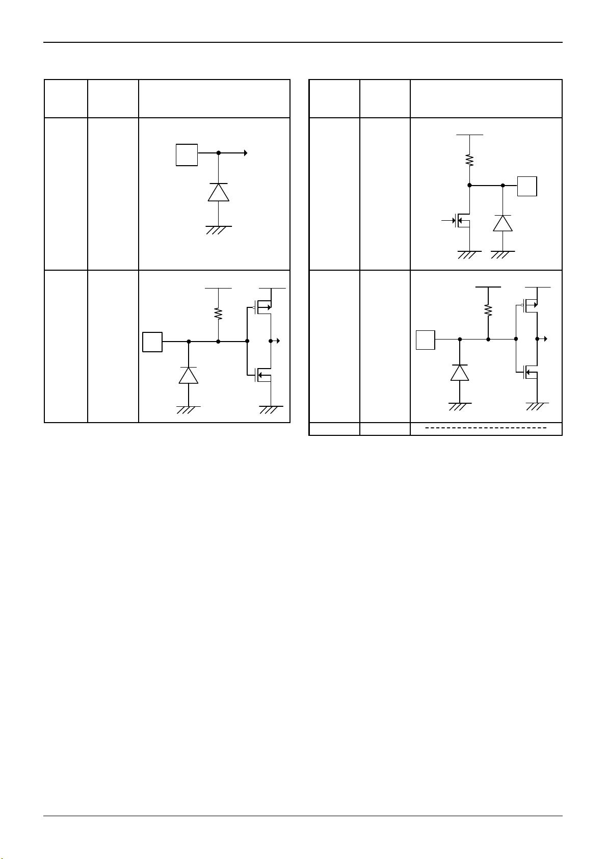
●Pin Function Diagram
Pin
No.
Pin
Name
Pin function Diagram
Pin
No.
Pin
Name
Technical Note
Pin function Diagram
VDD
VDD
1XTAL1
1
2
1. 2 M
Ω
100
Ω
8IO_C
2XTAL2
3
3VDD 9 RST
VDD
4CLKSEL
VDDP8VREG
11K
Ω
VREG
VREG
VREG
VDDP
9
VDDP
4,5
50K
5RSTIN
6IO_U 11 VCC
5
Ω
VDD VDD
11 K
Ω
10 CLK
7CGND
VDDP
1
Ω
10
VDDP
11
www.rohm.com
© 2009 ROHM Co., Ltd. All rights reserved.
5/15
2010.4 - Rev.D
Page 6
BD8918F,BD8918FV,BD8919F,BD8919FV
Technical Note
Pin No. Pin No.
Pin Name Pin function Diagram Pin Name Pin function Diagram
12
12 VDDP 14 OFFB
VDD
5KΩ
13 PRES 15
13
VDD
CMDVCCB
15
VDD
20KΩ
VDD
50KΩ
14
VDD
16 GND
www.rohm.com
© 2009 ROHM Co., Ltd. All rights reserved.
6/15
2010.4 - Rev.D
Page 7
BD8918F,BD8918FV,BD8919F,BD8919FV
5.0±0.2
10±0.2
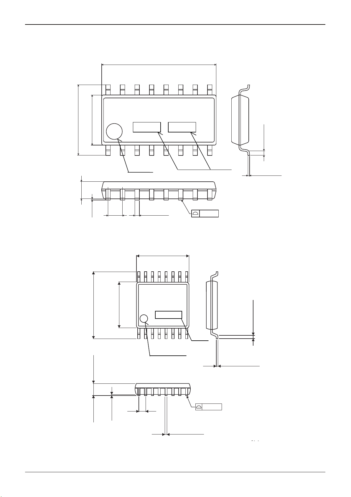
●Package
Package Name: SOP16 Note : X is 8 or 9.
Package Name: SSOP-B16
6.2± 0.3
1.5± 0.1
4.4± 0.2
0.11
6.4±0.3
1.15±0.1
(MAX 10.35 include BURR)
16
BD891XF
1
1PIN MARK
1.27
4.4±0.2
0.10
0.4± 0.1
Fig. 3.1 SOP16 Package Dimension
16
D891X
1
1PIN MARK
0.65
Fig. 3.2 SSOP-B16 Package Dimension
9
Lot No.
8
0.22±0.1
9
8
0.1
0.1
Lot No.
0.15± 0.1
(UNIT : mm)
0.3Min.
0.15±0.1
(UNIT : mm)
Technical Note
0.3MIN
www.rohm.com
© 2009 ROHM Co., Ltd. All rights reserved.
7/15
2010.4 - Rev.D
Page 8

BD8918F,BD8918FV,BD8919F,BD8919FV
●Function
1) Power supply
Power supply pins are VDD and VDDP. Set VDD at the same voltage as the signal from the system controller side.
VDDP and CGND are for the 5V power source and GND, respectively, on the card side.
2) Input voltage detector
The IC remains in wait mode until the power on reset is released 16ms after the VDD supply voltage is increased over
Vthd and the VDDP supply voltage is increased over Vthp, making the CMDVCCB signal turn from H to L.
Vthd=1.7V(typ) Vthp=2.25V(typ)
3) Operation sequence
3-1) Wait mode
The IC remains in wait mode until the power on reset is released after the VDD supply voltage is increased over Vthd and
the VDDP supply voltage is increased over Vthp, making the CMDVCCB signal turn from H to L.
In this mode, the VDD and VDDP supply voltage detector (VDET), thermal shutdown circuit (TSD), reference circuit
(VREF) and crystal oscillation circuit (XT OSC) are activated.
IO_U is pulled up to VDD with an 11k resistor and all the card contact pins are at Lo level.
3-2) Card presence
Card presence is detected by PRES pin. When the PRES pin is active, a card is assumed to be present.
Technical Note
Table 1
PRES “High” active
When a card is present in wait mode, the card insertion identification pin, PRES (“H” active) becomes active and OFFB
becomes “H” after approx. 8ms (debounce time).
If a card is present before the VDD and VDDP power sources are applied and the internal reset is released, it is internally
reset and OFFB becomes “H” after the debounce time.
The PRES pin is pulled up to VDD with a 50k resistor.
Descriptions of transition times (example. Debounce time: 8msec) for the operation
sequences are adapted in the conditions of the following input frequency.
www.rohm.com
© 2009 ROHM Co., Ltd. All rights reserved.
8MHz (BD8918F/ FV), 16MHz (BD8919F/ FV)
8/15
2010.4 - Rev.D
Page 9
BD8918F,BD8918FV,BD8919F,BD8919FV
Technical Note
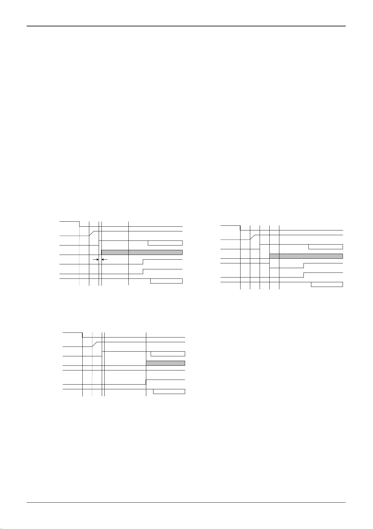
3-3) Activation sequence
When OFFB is in the “High” state and the CMDVCCB signal from the controller turns from H to L, the activation sequence
starts to activate each functional block in the following order:
The RST outputs signals based on the RSTIN input, being reset approximately 472sec after the CMDVCCB signal turns
from H to L. The RSTIN input becomes effective approximately 48s after I/O TRANS turns ON. If RSTIN becomes Lo
after RSTIN becomes effective and the RST output is released, the CLK signal is output. If RSTIN is High when the RST
output is released, the CLK signal is output as soon as the RST output is released. (Refer to Fig. 4-1, 4-2 and 4-3)
LDO ON (VCC output)
I/O TRANS ON (IO_C, IO_U Bus: Pull-up)
__________________________________________________
When RSTIN remains High until RST is released
(RSTINAlways High) (RSTIN=Always High)
CLK BUF ON (CLK output) CLK, RST BUF ON (CLK output, RST release)
RST BUF ON (RST release)
[Activation sequence under different RSTIN input timings]
CMDVCCB
VCC
IO_C
CLK
RSTIN
RST
IO_U
t0
t1 t2 t3
Min:200ns
t4= tact
ART
CMDVCCB
VCC
IO_C
CLK
RSTIN
RST
IO_U
t0
t1 t2 t3 t4= tact
Fig. 4-1 Activation sequence 1 Fig. 4-2 Activation sequence 2
CMDVCCB
VCC
IO_C
CLK
RSTIN
RST
IO_U
t0
t1 t2 t3 t4= tact
ART
t1: LDO startup time = typ. 24µs
Fig.6-3 立ち上げシーケンス 3
t2: I/O ON time = typ. 424µs
t3: CLK output release time (t3-t2) = Min. 200ns
t4: RST release time = typ,472µs, max.
481s
(Activation time)
Fig. 4-3 Activation sequence 3
(RSTIN input sequence not specified by ISO7816)
ART
www.rohm.com
© 2009 ROHM Co., Ltd. All rights reserved.
9/15
2010.4 - Rev.D
Page 10

BD8918F,BD8918FV,BD8919F,BD8919FV
Technical Note
3-4) Deactivation sequence
When the CMDVCCB input turns from L to H or the alarm signal (described later) is detected, the following deactivation
sequence is initiated in the following order, transitioning to the wait mode.
RST BUF OFF (RST: Lo)
CLK BUF OFF (CLK: Lo)
I/O TRANS OFF (I/O Bus on the controller side: Pull-up)
(I/O Bus on the card side: Lo)
LDO OFF (VCC: Lo)
CMDVCCB
RST
CLK
I/O
t11: CLK OFF time = typ. 10µs
t12: I/O OFF time = typ. 20μs
t13: Starting time of VCC fall = typ. 30μs
tde: Operational sequence completion time =Max. 200μs
VCC
t10
t11 t12
tde
t13
Fig. 5 Deactivation sequence
4) LDO
LDO supplies power to the IC card through VCC pin.
This regulator has a built-in over-current limiter circuit. It generates an internal alarm with a load current of approximately
140mA or more and enters into the deactivation sequence. Also, the output voltage is regarded as abnormal if it drops to
less than 1.6V and the output current is shut off; an internal alarm signal is generated and the deactivation sequence is
initiated.
Connect a capacitor of 1µF or 2.2µF between VCC and CGND as close as possible to the VCC pin, in order to reduce
the output voltage variation as much as possible. Also, ensure that ESR is kept at less than 100m.
LDO output is also a power source for CLK, RST and IO_C output. Therefore, the CLK, RST and IO_C output level is the
same as the VCC output level.
5) I/O data transitions
The data line, IO_C - IO_U, transmits/receives two-way data.
The IO_U pin for the controller side is pulled up with an 11k resistor to High (VDD voltage) and card contact pins IO_C
is set to Lo until I/O TRANS becomes ON by the activation sequence.
When I/O TRANS becomes On, IC becomes idle mode and the I/O pin is pulled up with an 11k resistor to keep the
IO_U pin to VDD voltage (High) and the IO_C pin to VCC voltage (High).
The pin which turns to L from H first becomes the master and the other output side becomes the slave between the pins
on the controller side and card contact pins. Then the data are transferred from the master side to the slave side.
When the both signal levels become High, they become idle mode.
When the signal transits from L to H and it passes over a threshold, an active pull-up (100 ns or less) works to drive the
data High at high speed. After the active pull-up is completed, the pin is pulled up with an 11k resistor. After the active
pull-up is completed, the pin is pulled up with an 11k resistor. This function enables signal transmission up to 1MHz.
Also, an over-current limiter of 30mA in the card contact pin, IO_C.
www.rohm.com
© 2009 ROHM Co., Ltd. All rights reserved.
10/15
2010.4 - Rev.D
Page 11

BD8918F,BD8918FV,BD8919F,BD8919FV
Technical Note
6) Card clock supply
Card clock is supplied from the CLK pin dividing the input frequency of XTAL1 pin with the CLKSEL pin setting. The clock
division switching time is within the 8 clocks of the XTAL1 signal.
The input signal to the XTAL1 pin is made by a crystal oscillator (BD8918F/FV:8Hz, BD8919F/FV:16MHz) between the
XTAL1 pin and XTAL2 pin or external pulse signal.
When a crystal oscillator is used, the voltage between XTAL1 and XTAL2 may decrease to become close to “-1V”, which
is not a problem.
When an external pulse signal is applied to the XTAL1 pin (except for signal input by crystal oscillation), the duty of the
XTAL1 pin should be 48% - 52% and the transition time of the XTAL1 pin should be within 5% of the signal cycle to
ensure the duty factor of 45% - 55% at the CLK pin.
Table 2 Clock frequency selection (f
BD8918F/FV
CLKSEL f
1
0
: Frequency at XTAL1)
XTAL
clk
f
XTAL
f
XTAL
2
BD8919F/FV
CLKSEL f
1
0
f
f
XTAL
XTAL
7) RSTIN input, RST output
The RSTIN input becomes effective after the CMDVCCB signal input turns to L from H, activation sequence is initiated
and approximately 48s after I/O TRANS turns ON. The RST output is released in approximately 472sec (max.
481sec) after the CMDVCCB signal turns from H to L to output a signal based on the RSTIN input.
8) Fault detection
When the following fault state is detected, the circuit enters the wait mode after it generates an internal alarm signal and
is deactivated.
If a card is not present, it remains in the wait mode.
• When the VCC pin becomes less than 1.6V, or is loaded high current (TYP: 140mA)
• When VDDP voltage is less than the threshold voltage (detected by supply voltage detector)
• When a high temperature is detected by the thermal shutdown circuit
• When the card is removed during operation or the card is not present from the beginning (PRES=L)
9) OFFB output
The OFFB output pin indicates the IC is ready to operate. It is pulled up to VDD with a 20k resistor.
When the IC is in the ready state, OFFB is High.
After activation, the OFFB outputs OFF state (Lo) when a fault state is detected.
When a card is present and CMDVCCB becomes High, the internal alarm is released and the OFFB output becomes
High.
PRES
OFFB
CMDVCCB
t
VCC
debounce
t
debounce
t
debounce
Shutdown by card removal Shutdown by short-circuiting of pins
端子ショート等による停止動作カード取り外しによる停止動作
Fig. 6 OFFB, CMDVCCB, PRES, VCC operation
clk
2
4
= typ 8ms
www.rohm.com
© 2009 ROHM Co., Ltd. All rights reserved.
11/15
2010.4 - Rev.D
Page 12

BD8918F,BD8918FV,BD8919F,BD8919FV
●An example of software control
Start
OFFB=H ?
No (No card)
Yes (Card detect)
CMDVCCB: H→L
Activation start
↓
Regulator on (VCC)
↓
IO enable (IO)
Card communication start
RSTIN: L→H
↓
Complete
CMDVCCB: L→H
No alarm
Error message 2
・Detects error at card
communication
Deactivation start
↓
IO disable (IO)
↓
Regulator off (VCC)
End
Fig. 7 An example of software control
Error message 1
・Card insert
OFFB=L ?
Deactivation start
IO disable (IO)
Regulator off (VCC)
CMDVCCB: L→H
End
Alarm detect
・Card off
・Over current
・Drop VDDP
・Thermal
shutdown
↓
↓
End
* Ensure to set CMDVCCB LH to confi rm that LSI
could detect alarm at the host side
Technical Note
www.rohm.com
© 2009 ROHM Co., Ltd. All rights reserved.
12/15
2010.4 - Rev.D
Page 13

BD8918F,BD8918FV,BD8919F,BD8919FV
_
●Application examples
BD8918F/FV application examples
CONTROLLER
+3.3V
(22pF)
(22pF
)
8MHz
220Ω
XTAL1
XTAL2
VDD
CLKSEL
RSTIN
IO_U
CGND
IO_C
+3. 3V
XTAL 1 GND
VDD
CLKSEL
RSTIN
IO_U
CGND
IO
0.1µF
1
2
3
BD8918F/
4
BD8918FV
5
6
7
8
CARD CONNECTION
1µF
0.22µF
C5C6C1
C7
C8C3C4
16
15
14
13
12
11
10
9
C2
K1
K2
Fig.8
CONTROLLER
0.1uF
1
2
3
BD8918F/
4
BD8918FV
5
6
7
C
8
1uF
CARD CONNECTION
0.2 2 uF
C5C6C1
C2
C7C8C3
C4
K1
K2
Fig.9
GND
CMDVCCB
OFFB
PRES
VDDP
VCC
CLK
RST
16
CMDVCCB
15
OFFB
14
13
VDDP
12
11
10
9
PRES
VCC
CLK
RST
Technical Note
10µF
+5V
10uF
+5V
www.rohm.com
© 2009 ROHM Co., Ltd. All rights reserved.
13/15
2010.4 - Rev.D
Page 14

BD8918F,BD8918FV,BD8919F,BD8919FV
Technical Note
BD8919F/FV application examples
CONTROLLER
+3.3V
(22pF)
(22pF)
16MHz
220Ω
XTAL1
XTAL2
VDD
CLKSEL
RSTIN
IO_U
CGND
IO_C
0.1µF
1
2
3
BD8919F/
4
BD8919FV
5
6
7
8
GND
16
CMDVCCB
15
OFFB
14
PRES
13
VDDP
12
VCC
11
CLK
10
RST
9
10µF
+5V
1µF
CARD CONNECTION
0.22µF
C5C6C1
C2
C7
C8C3C4
K1
K2
●Precautions for use
1) The capacitor for the VCC pin should be placed as close as possible to the IC between VCC and CGND so that the ESR
becomes less than 100Ω
2) Connect a capacitor of over 0.1µF for VDD and over 10µF for VDDP as close as possible to the IC so that the ESR
becomes less than 100m to reduce the power line noise. We recommend the use of capacitors with the largest possible
capacitance.
www.rohm.com
© 2009 ROHM Co., Ltd. All rights reserved.
14/15
2010.4 - Rev.D
Page 15

BD8918F,BD8918FV,BD8919F,BD8919FV
Ordering part number
B D 8 9 1 8 F V - E 2
Part No.
SOP16
SSOP-B16
Part No.
8918
8919
10± 0.2
(MAX 10.35 include BURR)
16
4.4± 0.2
6.2± 0.3
1
1.5± 0.1
1.27
0.10
0.4± 0.1
5.0±0.2
16
4.4±0.2
1
0.65
0.11
6.4±0.3
1.15±0.1
9
0.3MIN
8
0.15± 0.1
0.1
(Unit : mm)
9
0.3Min.
8
0.15±0.1
0.1
0.22±0.1
(Unit : mm)
Package
F: SOP16
FV: SSOP-B16
<Tape and Reel information>
Embossed carrier tapeTape
Quantity
Direction
of feed
<Tape and Reel information>
Quantity
Direction
of feed
2500pcs
E2
The direction is the 1pin of product is at the upper left when you hold
()
reel on the left hand and you pull out the tape on the right hand
Reel
Embossed carrier tapeTape
2500pcs
E2
The direction is the 1pin of product is at the upper left when you hold
()
reel on the left hand and you pull out the tape on the right hand
Reel
Packaging and forming specification
E2: Embossed tape and reel
1pin
Order quantity needs to be multiple of the minimum quantity.
∗
1pin
Order quantity needs to be multiple of the minimum quantity.
∗
Technical Note
Direction of feed
Direction of feed
www.rohm.com
© 2009 ROHM Co., Ltd. All rights reserved.
15/15
2010.4 - Rev.D
Page 16

Notes
No copying or reproduction of this document, in part or in whole, is permitted without the
consent of ROHM Co.,Ltd.
The content specied herein is subject to change for improvement without notice.
The content specied herein is for the purpose of introducing ROHM's products (hereinafter
"Products"). If you wish to use any such Product, please be sure to refer to the specications,
which can be obtained from ROHM upon request.
Examples of application circuits, circuit constants and any other information contained herein
illustrate the standard usage and operations of the Products. The peripheral conditions must
be taken into account when designing circuits for mass production.
Great care was taken in ensuring the accuracy of the information specied in this document.
However, should you incur any damage arising from any inaccuracy or misprint of such
information, ROHM shall bear no responsibility for such damage.
The technical information specied herein is intended only to show the typical functions of and
examples of application circuits for the Products. ROHM does not grant you, explicitly or
implicitly, any license to use or exercise intellectual property or other rights held by ROHM and
other parties. ROHM shall bear no responsibility whatsoever for any dispute arising from the
use of such technical information.
Notice
The Products specied in this document are intended to be used with general-use electronic
equipment or devices (such as audio visual equipment, ofce-automation equipment, communication devices, electronic appliances and amusement devices).
The Products specied in this document are not designed to be radiation tolerant.
While ROHM always makes efforts to enhance the quality and reliability of its Products, a
Product may fail or malfunction for a variety of reasons.
Please be sure to implement in your equipment using the Products safety measures to guard
against the possibility of physical injury, re or any other damage caused in the event of the
failure of any Product, such as derating, redundancy, re control and fail-safe designs. ROHM
shall bear no responsibility whatsoever for your use of any Product outside of the prescribed
scope or not in accordance with the instruction manual.
The Products are not designed or manufactured to be used with any equipment, device or
system which requires an extremely high level of reliability the failure or malfunction of which
may result in a direct threat to human life or create a risk of human injury (such as a medical
instrument, transportation equipment, aerospace machinery, nuclear-reactor controller, fuelcontroller or other safety device). ROHM shall bear no responsibility in any way for use of any
of the Products for the above special purposes. If a Product is intended to be used for any
such special purpose, please contact a ROHM sales representative before purchasing.
If you intend to export or ship overseas any Product or technology specied herein that may
be controlled under the Foreign Exchange and the Foreign Trade Law, you will be required to
obtain a license or permit under the Law.
www.rohm.com
© 2010 ROHM Co., Ltd. All rights reserved.
Thank you for your accessing to ROHM product informations.
More detail product informations and catalogs are available, please contact us.
ROHM Customer Support System
http://www.rohm.com/contact/
R1010
A
 Loading...