

A
Headphone Amplifiers
Coupling Capacitorless
Headphone Amplifiers
BD88400GUL,BD88410GUL,BD88415GUL,BD88420GUL
No.11102EAT04
●Description
BD88xxxGUL is output coupling capacitorless headphone amplifier. This IC has a negative voltage generator of regulated
type built-in and generates the direct regulated negative voltage from the supply voltage. It is possible to drive headphones
in a ground standard with both voltage of the positive voltage (+2.4V) and the negative voltage (-2.4V). Therefore a
large-capacity output coupling capacitor becomes needless and can reduce a cost, a board area, and the height of the part.
In addition, there is not the signal decrement by the low range to happen by output coupling capacitor and output load
impedance and can output a rich low tone.
●Features
1) 2.4V to 5.5V Single-Supply Operation
2) No Bulky DC-Blocking Capacitors Required
3) No Degradation of Low-Frequency Response Due to Output Capacitors
4) Ground-Referenced Outputs
5) Gain setting
BD88400GUL: Variable gain with external resistors
BD88410GUL: -1.0V/V
BD88415GUL: -1.5V/V
BD88420GUL: -2.0V/V
6) Low THD+N
7) Low Supply Current
8) Integrated Negative Power Supply
9) Integrated Short-Circuit and Thermal-Overload Protection
10) Small package
VCSP50L2 (2.1mm x 2.1mm)
●Applications
Mobile Phones, Smart Phones, PDAs, Portable Audio Players, PCs, TVs, Digital Cameras, Digital Video Cameras,
Electronic Dictionaries, Voice Recorders, Bluetooth Head-sets, etc
●Line up
Supply
Type
BD88400GUL
BD88410GUL -1.0
BD88415GUL -1.5
BD88420GUL -2.0
www.rohm.com
© 2011 ROHM Co., Ltd. All rights reserved.
Voltage
2.4~5.5
[V]
Supply
Current
[mA]
2.0
(No signal)
Gain
[V/V]
Variable gain
with external
resister
Maximum
Output Power
[mW]
(VDD=3.3V,RL=16Ω
THD+N≦1%,f=1kHz)
80
1/25
THD+N
[%]
0.006
(VDD=3.3V,RL=16Ω
Po=10mW,f=1kHz)
Noise
Voltage
[µVrms]
10
PSRR
[dB]
-80
(f=217Hz)
Package
VCSP50L2
(2.1mm x 2.1mm)
2011.03 – Rev.
BD88400GUL,BD88410GUL,BD88415GUL,BD88420GUL
A
●Absolute maximum ratings
Parameter Symbol Ratings Unit
Technical Note
SGND to PGND voltage
SVDD to PVDD voltage
SVSS to PVSS voltage
SGND or PGND to SVDD, PVDD voltage
SVSS, PVSS to SGND or PGND voltage
SGND to IN_- voltage
SGND to OUT_- voltage
PGND to C1P- voltage
PGND to C1N- voltage
SGND to SHDN_B- voltage
Input current
Power Dissipation
Storage Temperature Range
* In operating over 25 ℃, de-rate the value to 10.8mW/℃. This value is for mounted on the application board
(Grass-epoxy, size: 40mm x 60mm, H=1.6mm, Top Copper area = 79.9%, Bottom Copper area = 80.2%).
VGG 0.0 V
VDD -0.3~0.3 V
VSS 0.0 V
VDG -0.3~6.0 V
VSG
-3.5~0.3
VIN (SVSS-0.3)~2.8 V
V
OUT
(PGND-0.3)~(PVDD+0.3) V
V
C1P
V
C1N
(SVSS-0.3)~2.8
(PVSS-0.3)~(PGND+0.3)
VSH (SGND-0.3)~(SVDD+0.3) V
IIN
-10~10
PD 1350 * mW
T
STG
-55~150 ℃
●Operating conditions
Parameter Symbol
Min. Typ. Max.
Ratings
V
V
V
mA
Unit
Supply Voltage Range
Operating Temperature Range
V
SVDD,VPVDD
T
OPR
2.4 - 5.5 V
-40 - +85 ℃
www.rohm.com
© 2011 ROHM Co., Ltd. All rights reserved.
2/25
2011.03 – Rev.
BD88400GUL,BD88410GUL,BD88415GUL,BD88420GUL
A
●Electrical characteristics
Unless otherwise specified, Ta=25℃, SVDD=PVDD=3.3V, SGND=PGND=0V, SHDNB=SVDD, C1=C2=2.2µF,
RL=No Load, Ri=Rf=10kΩ
Parameter Symbol
Min. Typ. Max.
Limits
Unit Conditions
Supply Current
Shutdown Supply Current IST - 0.1 2 µA SHDNLB=SHDNRB=L
Technical Note
(SHDNLB,SHDNRB)=(H,L) or (L,H),
No signal
SHDNLB=SHDNRB=H,
No signal
Quiescent Supply Current
- 1.3 - mA
I
DD1
I
- 2.0 7.4 mA
DD2
SHDN_B Terminal
H Level Input Voltage VIH 1.95 - - V
L Level Input Voltage VIL - - 0.70 V
Input Leak Current I
- - ±1 µA
LEAK
Headphone Amplifier
Shutdown to Full Operation t
- 80 - µs SHDNLB=SHDNRB=L→H
SON
Offset Voltage VIS - ±0.5 ±5.0 mV
30 60 - mW
Maximum Output Power P
OUT
40 80 - mW
Total Harmonic Distortion
+ Noise
THD+N
- 0.008 0.056 %
- 0.006 0.100 %
Input Impedance ZIN 10 14 19 kΩ
RL=32Ω, THD+N≦-40dB, f=1kHz,
20kHz LPF, for Single Channel
RL=16Ω, THD+N≦-40dB, f=1kHz,
20kHz LPF, for Single Channel
RL=32Ω, POUT=10mW, f=1kHz,
20kHz LPF
RL=16Ω, POUT=10mW, f=1kHz,
20kHz LPF
SHDNLB=SHDNRB=H
In BD88400GUL, ZIN = Ri
Gain
BD88400GUL
BD88410GUL -1.05 -1.00 -0.95
AV
BD88415GUL -1.55 -1.50 -1.45
- -1.00 -
In BD88400GUL, Gain is variable
V/V
by the external resister of Ri and Rf.
BD88420GUL -2.06 -2.00 -1.94
Gain match ΔAV - 1 - %
Noise VN - 10 - µVrms 20kHz LPF + JIS-A
Slew Rate SR - 0.15 - V/µs
Maximum Capacitive Load CL - 200 - pF
Crosstalk CT - -90 - dB
Power Supply
Rejection Ratio
Charge-Pump
Oscillator Frequency
PSRR - -80 - dB
f
200 300 430 kHz
OSC
RL=32Ω, f=1kHz, VOUT=200mV
1kHz BPF
f=217Hz, 100mV
P-P
217Hz BPF
Thermal-Shutdown Threshold TSD - 145 - ℃
Thermal-Shutdown Hysteresis T
- 5 - ℃
HYS
‐ripple,
P-P
,
www.rohm.com
© 2011 ROHM Co., Ltd. All rights reserved.
3/25
2011.03 – Rev.
BD88400GUL,BD88410GUL,BD88415GUL,BD88420GUL
A
]
Technical Note
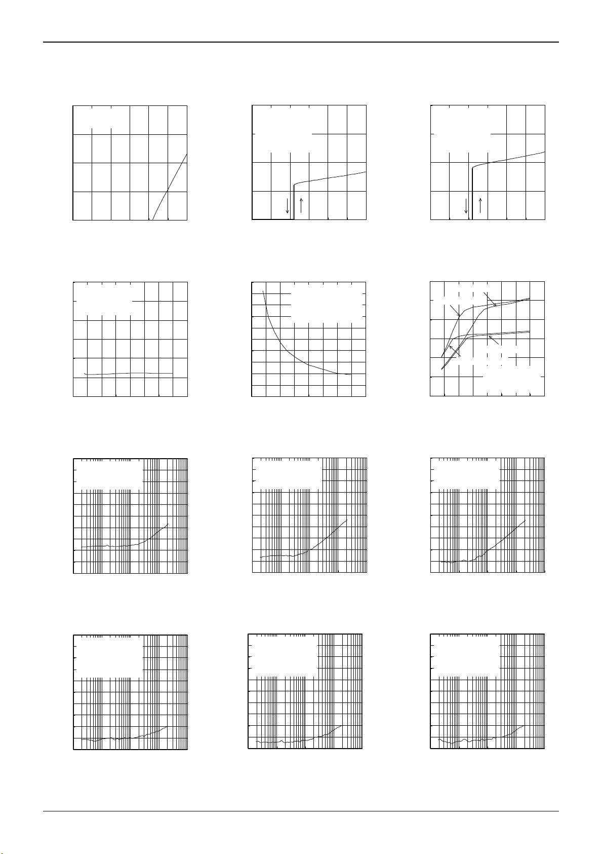
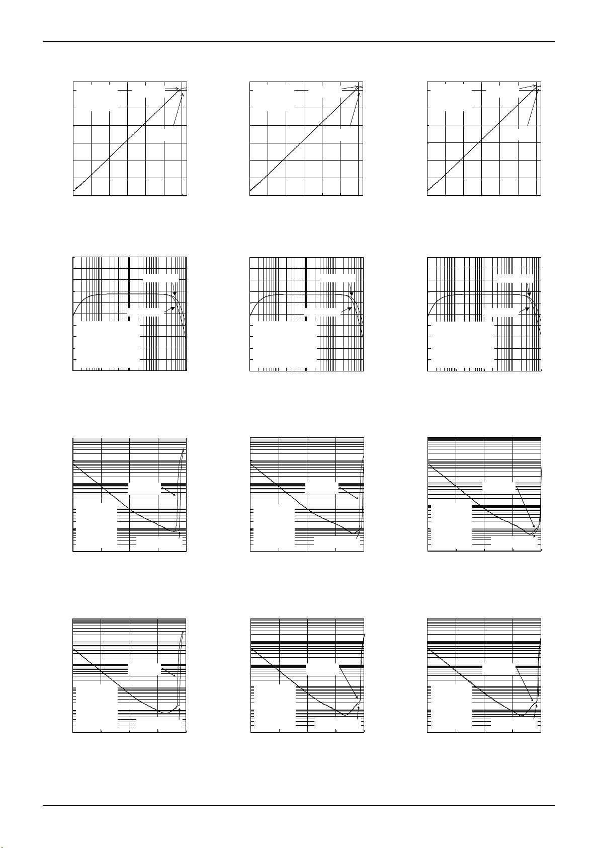
●Electrical characteristic curves – General Items (Reference data)
Unless otherwise specified, Ta=25℃, SGND=PGND=0V, SHDNLB=SHDNRB=SVDD, C1=C2=2.2µF,
Input coupling capacitor=1µF, RL=No Load
1u
SHDNLB=0V
SHDNRB=0V
100n
10n
* In BD88400GUL the input resister(Ri)=10kΩ, feedback resister(Rf)=10kΩ.
4.0
SHDNLB=VDD
SHDNRB=0V
* This caracteristics has
3.0
hyster esis (40mV typ) by
UVL O.
2.0
4.0
SHDNLB=VDD
SHDNRB=VDD
* This caracteristics has
3.0
hyster esis (40mV typ) by
UVL O.
2.0
Standby Current [A
1n
1.0
Operating Current [mA]
Operating Current [mA]
1.0
0.1n
0.0 1.0 2.0 3.0 4.0 5.0 6.0
Fig.1 Standby Current vs.
0
-0.5
-1
Supply V oltage [V]
Supply Voltage
SHDNLB=VDD
SHDNRB=VDD
No L oad
-1.5
-2
VSS Voltage [V]
-2.5
-3
2.0 2.5 3.0 3.5 4.0 4.5 5.0 5.5 6.0
Fig.4 Negative Voltage vs.
0
-10
-20
-30
-40
-50
-60
PSRR [dB]
-70
-80
-90
-100
10 100 1k 10k 100k
Fig.7 PSRR vs. Frequency
0
-10
-20
-30
-40
-50
-60
PSRR [dB]
-70
-80
-90
-100
10 100 1k 10k 100k
Supply V oltage [V]
Supply Voltage
VDD=2.4V
Ripple = 100mVp-p
BPF
Frequency [Hz]
(VDD=2.4V)
VDD=2.4V
VOUT = 200mVp-p
RL=32
Ω
BPF
Frequency [Hz]
Fig.10 Crosstalk vs.
© 2011 ROHM Co., Ltd. All rights reserved.
Frequency (VDD=2.4V)
www.rohm.com
0.0
0.0 1.0 2.0 3.0 4.0 5.0 6.0
Supply V oltage [V]
Fig.2 Monaural Operating
Current vs. Supply Voltage
200
180
160
140
120
100
80
Setup time [us]
60
40
20
0
2.0 2.5 3.0 3.5 4.0 4.5 5.0 5.5 6.0
SHDNLB =SHDNRB
=L->H
VSS 90% Setup time
No Load
Supply V oltage [V]
Fig.5 Setup time vs.
Supply Voltage
0
VDD=3.3V
-10
Ripple = 100mVp-p
-20
BPF
-30
-40
-50
-60
PSRR [dB]
-70
-80
-90
-100
10 100 1k 10k 100k
Frequency [Hz]
Fig.8 PSRR vs. Frequency
(VDD=3.3V)
0
VDD=3.3V
-10
VOUT = 200mVp-p
-20
RL=32
-30
-40
-50
-60
PSRR [dB]
-70
-80
-90
-100
10 100 1k 10k 100k
Ω
BPF
Frequency [Hz]
Fig.11 Crosstalk vs.
Frequency (VDD=3.3V)
4/25
0.0
0.0 1.0 2.0 3.0 4.0 5.0 6.0
Supply V oltage [V]
Fig.3 Stereo Operating
Current vs. Supply voltage
120
100
80
60
40
20
Maximum Output Po wer [mW]
0
2.0 2.5 3.0 3.5 4.0 4.5 5.0 5.5 6.0
RL=16Ω, in phase
RL=16Ω, out of phase
RL=32Ω, in phase
RL=32Ω, out of phase
THD+N≦-40d B
20kHz LPF
Stereo
Supply V oltage [V]
Fig.6 Maximum power vs.
Supply Voltage
0
VDD=5.5V
-10
Ripple = 100mVp-p
-20
BPF
-30
-40
-50
-60
PSRR [dB]
-70
-80
-90
-100
10 100 1k 10k 100k
Fre quency [H z]
Fig.9 PSRR vs. Frequency
(VDD=5.5V)
0
VDD=5.5V
-10
VOUT = 200mVp-p
-20
RL=32
-30
-40
-50
-60
PSRR [dB]
-70
-80
-90
-100
Ω
BPF
10 100 1k 10k 100k
Frequency [Hz]
Fig.12 Crosstalk vs.
Frequency (VDD=5.5V)
2011.03 – Rev.
BD88400GUL,BD88410GUL,BD88415GUL,BD88420GUL
A
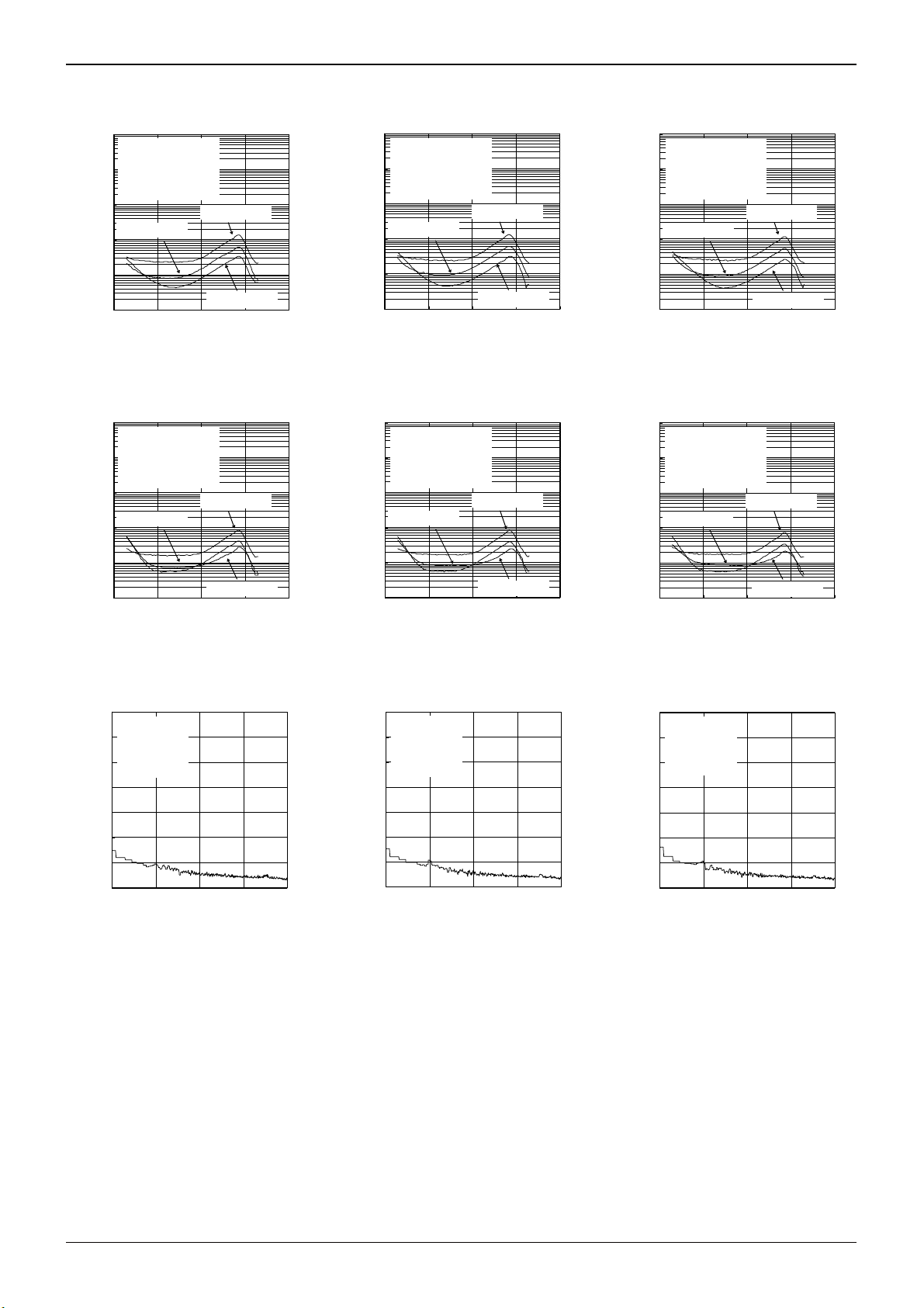
●Electrical characteristic curves – BD88415GUL (Reference data)
0
-20
VDD=2.4V
f=1kHz
BPF
RL=32
VDD=3.3V
-20
0
f=1kHz
BPF
Ω
RL=32
Ω
-40
-60
-80
Output V olta ge [dBV]
-100
-120
-120 -100 -80 -60 -40 -20 0
Fig.13 Output Voltage vs.
Input Voltage (VDD=2.4V)
10
8
6
4
2
0
Gain [dB]
-2
-4
-6
-8
-10
10 100 1k 10k 100k
Fig.16 Gain vs. Frequency
Input Voltage [dBV]
VDD=2.4V
Po=10mW
RL=16
Ω
Input coupling
capacitor = 1.0uF
Frequency [Hz]
(VDD=2.4V)
RL=32
RL=16
RL=16
Ω
Ω
Ω
-40
-60
-80
Output V olta ge [dBV]
-100
-120
-120 -100 -80 -60 -40 -20 0
Input Voltage [dBV]
RL=16
Fig.14 Output Voltage vs.
Input Voltage (VDD=3.3V)
10
8
6
4
2
0
Gain [dB]
-2
VDD=3.3V
Po=10mW
-4
RL=16
-6
-8
-10
10 100 1k 10k 100k
Ω
Input coupling
capacitor = 1.0uF
Frequency [Hz]
RL=16
RL=32
Fig.17 Gain vs. Frequency
(VDD=3.3V)
Ω
Ω
Ω
100
100
10
10
1
0.1
THD+N [%]
VDD=2.4V
20kHz-LP F
f=1kHz
0.01
Stereo
RL=16
0.001
1n 100n 10u 1m 100m
Fig.19 THD+N vs. Output
Power (VDD=2.4V, RL=16Ω)
100
In p hase
Ω
Output P owe r [W]
Out of phase
1
0.1
THD+N [%]
VDD=3.3V
20kHz-LP F
f=1kHz
0.01
Stereo
RL=16
0.001
1n 100n 10u 1m 100m
In p hase
Ω
Output P owe r [W]
Out of phase
Fig.20 THD+N vs. Output
Power (VDD=3.3V, RL=16Ω)
100
10
1
0.1
THD+N [%]
VDD=2.4V
20kHz-LP F
f=1kHz
0.01
Stereo
RL=32
0.001
1n 100n 10u 1m 100m
In p hase
Ω
Output P ower [W]
Fig.22 THD+N vs. Output
Power (VDD=2.4V, RL=32Ω)
Out of phase
10
1
0.1
THD+N [%]
VDD=3.3V
20kHz-LP F
f=1kHz
0.01
Stereo
RL=32
0.001
1n 100n 10u 1m 100m
Ω
In p hase
Out of phase
Output P ower [W]
Fig.23 THD+N vs. Output
Power (VDD=3.3V, RL=32Ω)
Technical Note
VDD=5.5V
0
f=1kHz
BPF
-20
-40
-60
-80
Output V olta ge [dBV]
-100
-120
-120 -100 -80 -60 -40 -20 0
Fig.15 Output Voltage vs.
Input Voltage (VDD=5.5V)
10
8
6
4
2
0
Gain [dB]
-2
VDD=5.5V
Po=10mW
-4
RL=16
-6
-8
-10
Ω
Input coupling
capacitor = 1.0uF
10 100 1k 10k 100k
Fig.18 Gain vs. Frequency
(VDD=5.5V)
100
10
1
0.1
THD+N [%]
VDD=5.5V
20kHz-LP F
f=1kHz
0.01
Stereo
RL=16
0.001
Ω
1n 100n 10u 1m 100m
Fig.21 THD+N vs. Output
Power (VDD=5.5V, RL=16Ω)
100
10
1
0.1
THD+N [%]
VDD=5.5V
20kHz-LP F
f=1kHz
0.01
Stereo
RL=32
0.001
Ω
1n 100n 10u 1m 100m
Fig.24 THD+N vs. Output
Power (VDD=5.5V, RL=32Ω)
RL=32
RL=16
Input Voltage [dBV]
RL=16
RL=32
Frequency [Hz]
In p hase
Out of phase
Output P owe r [W]
In p hase
Out of phase
Output P ower [W]
Ω
Ω
Ω
Ω
www.rohm.com
© 2011 ROHM Co., Ltd. All rights reserved.
5/25
2011.03 – Rev.
BD88400GUL,BD88410GUL,BD88415GUL,BD88420GUL
A
●Electrical characteristic curves – BD88415GUL (Reference data) – Continued
100
10
1
0.1
THD+N [%]
VDD=2.4V
RL=16
Ω
20kHz-LP F
Stereo (in phase)
Po=1mW
Po=0.1mW
100
10
1
0.1
THD+N [%]
VDD=3.3V
RL=16Ω
20kHz-LPF
Ste reo (in phase )
Po=0.1mW
Po=1mW
0.01
0.001
10 100 1k 10k 100k
Fig.25 THD+N vs. Frequency
(VDD=2.4V, RL=16Ω)
Frequency [Hz]
Po=10mW
0.01
0.001
10 100 1k 10k 100k
Po=10mW
Frequency [Hz]
Fig. 26 THD+N vs. Frequency
(VDD=3.3V, RL=16Ω)
100
10
1
0.1
THD+N [%]
VDD=2.4V
RL=32
Ω
20kHz-LP F
Stereo (in phase)
Po=10mW
Po=0.1mW
100
10
1
0.1
THD+N [%]
VDD=3.3V
RL=32Ω
20kHz-LPF
Ste reo (in phase )
Po=0.1mW
Po=10mW
0.01
0.001
10 100 1k 10k 100k
Fig. 28 THD+N vs. Frequency
(VDD=2.4V, RL=32Ω)
Frequency [Hz]
Po=1mW
0.01
0.001
10 100 1k 10k 100k
Frequency [Hz]
Po=1mW
Fig. 29 THD+N vs. Frequency
(VDD=3.3V, RL=32Ω)
0
VDD=2.4V
-20
Input connect
to the ground
-40
with 1uF
-60
-80
Spectrum [dB V]
-100
-120
-140
10 100 1k 10k 100k
Frequency [Hz]
Fig.31 Noise Spectrum
(VDD=2.4V)
0
VDD=3.3V
-20
Input connect
to the ground
-40
with 1 uF
-60
-80
Spectrum [dBV]
-100
-120
-140
10 100 1k 10k 100k
Frequency [Hz]
Fig.32 Noise Spectrum
(VDD=3.3V)
Technical Note
100
VDD=5.5V
RL=16Ω
10
20kHz-LPF
Ste reo (in phase )
1
Po=1mW
0.1
THD+N [%]
0.01
0.001
10 100 1k 10k 100k
Fig. 27 THD+N vs. Frequency
(VDD=5.5V, RL=16Ω)
100
VDD=5.5V
RL=32Ω
10
20kHz-LPF
Ste reo (in phase )
1
Po=10mW
0.1
THD+N [%]
0.01
0.001
10 100 1k 10k 100k
Fig. 30 THD+N vs. Frequency
(VDD=5.5V, RL=32Ω)
0
VDD=5.5V
-20
Input connect
to the ground
-40
with 1 uF
-60
-80
Spectrum [dBV]
-100
-120
-140
10 100 1k 10k 100k
Fig.33 Noise Spectrum
(VDD=5.5V)
Po=0.1mW
Po=10mW
Frequency [Hz]
Po=0.1mW
Po=1mW
Frequency [Hz]
Frequency [Hz]
www.rohm.com
© 2011 ROHM Co., Ltd. All rights reserved.
6/25
2011.03 – Rev.
BD88400GUL,BD88410GUL,BD88415GUL,BD88420GUL
A
●Electrical characteristic curves – BD88400GUL (Reference data)
VDD=3.3V
0
f=1kHz
BPF
-20
-40
-60
-80
Output V olta ge [dBV]
-100
-120
-120 -100 -80 -60 -40 -20 0
Input Voltage [dBV]
Fig.34 Output Voltage vs.
Input Voltage (VDD=3.3V)
100
10
1
0.1
THD+N [%]
VDD=3.3V
20kHz-LP F
f=1kHz
0.01
Stereo
RL=32
0.001
Ω
1n 100n 10u 1m 100m
Output P owe r [W]
Fig. 37 THD+N vs. Output
Power (VDD=3.3V, RL=32Ω)
RL=32
Ω
RL=16
In p hase
Out of phase
Ω
10
VDD=3.3V, Po=10mW
8
Ri=10kΩ, Input co upling
6
capacitor = 1.0uF
4
2
0
Gain [dB]
-2
-4
-6
-8
-10
10 100 1k 10k 100k
Frequency [Hz]
RL=16
RL=32
Fig.35 Gain vs. Frequency
(VDD=3.3V)
100
VDD=3.3V
RL=16Ω
10
20kHz-LPF
Ste reo (in phase )
1
Po=1mW
0.1
THD+N [%]
0.01
0.001
10 100 1k 10k 100k
Po=0.1mW
Frequency [Hz]
Fig.38 THD+N vs. Frequency
(VDD=3.3V, RL=16Ω)
Ω
Ω
Po=10mW
0
VDD=3.3V
-20
Input connect
to the ground
-40
with 1uF
-60
-80
Spectrum [dBV]
-100
-120
-140
10 100 1k 10k 100k
Frequency [Hz]
Fig.40 Noise Spectrum
(VDD=3.3V)
Technical Note
100
10
1
0.1
THD+N [%]
VDD=3.3V
20kHz-LP F
f=1kHz
0.01
Stereo
RL=16
0.001
Ω
1n 100n 10u 1m 100m
Output P ower [W]
Fig.36 THD+N vs. Output
Power (VDD=3.3V, RL=16Ω)
100
VDD=3.3V
RL=32Ω
10
20kHz-LPF
Ste reo (in phase )
1
Po=1mW
0.1
THD+N [%]
0.01
0.001
10 100 1k 10k 100k
Fig. 39 THD+N vs. Frequency
(VDD=3.3V, RL=32Ω)
In p hase
Out o f p hase
Po=0.1mW
Po=10mW
Frequency [Hz]
www.rohm.com
© 2011 ROHM Co., Ltd. All rights reserved.
7/25
2011.03 – Rev.

BD88400GUL,BD88410GUL,BD88415GUL,BD88420GUL
A
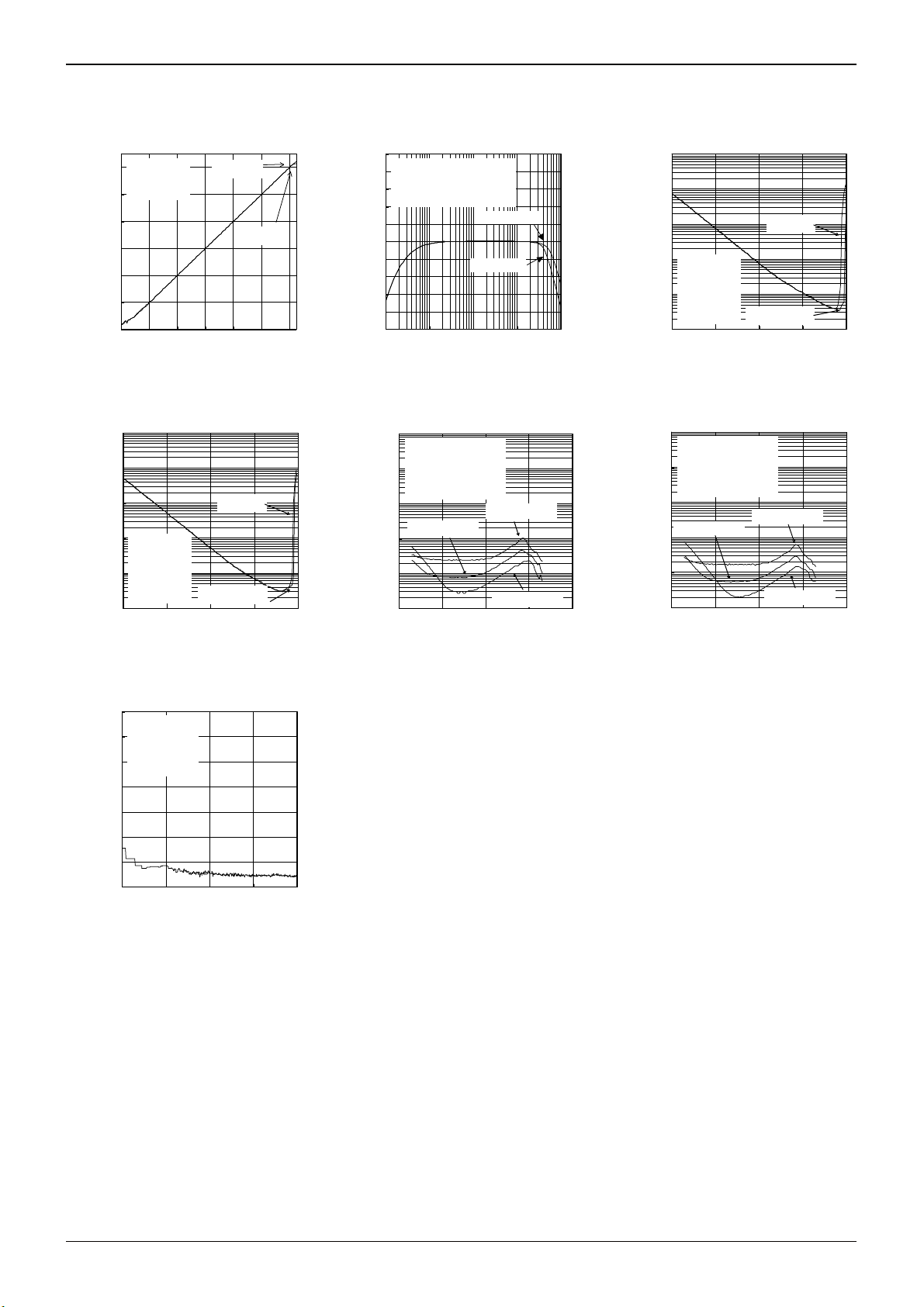
●Electrical characteristic curves – BD88410GUL (Reference data)
VDD=3.3V
0
f=1kHz
BPF
-20
-40
-60
-80
Output V olta ge [dBV]
-100
-120
-120 -100 -80 -60 -40 -20 0
RL=32
Input Voltage [dBV]
Fig.41 Output Voltage vs.
Input Voltage (VDD=3.3V)
100
10
1
In p hase
0.1
THD+N [%]
VDD=3.3V
20kHz-LP F
f=1kHz
0.01
Stereo
RL=32
0.001
Ω
1n 100n 10u 1m 100m
Output P ower [W]
Fig. 44 THD+N vs. Output
Power (VDD=3.3V, RL=32Ω)
Ω
RL=16
Ω
Out o f p hase
10
VDD=3.3V
8
Po=10mW
6
Input coupling
4
capacitor = 1.0uF
2
0
Gain [dB]
-2
-4
-6
-8
-10
10 100 1k 10k 100k
Frequency [Hz]
RL=16
RL=32
Fig.42 Gain vs. Frequency
(VDD=3.3V)
100
VDD=3.3V
RL=16Ω
10
20kHz-LPF
Ste reo (in phase )
1
Po=1mW
0.1
THD+N [%]
0.01
0.001
10 100 1k 10k 100k
Po=0.1mW
Po=10mW
Frequency [Hz]
Fig.45 THD+N vs. Frequency
(VDD=3.3V, RL=16Ω)
Ω
Ω
0
VDD=3.3V
-20
Input connect
to the ground
-40
with 1uF
-60
-80
Spectrum [dBV]
-100
-120
-140
10 100 1k 10k 100k
Frequency [Hz]
Fig.47 Noise Spectrum
(VDD=3.3V)
Technical Note
100
10
1
0.1
THD+N [%]
VDD=3.3V
20kHz-LP F
f=1kHz
0.01
Stereo
RL=16
0.001
Ω
1n 100n 10u 1m 100m
Output P ower [W]
Fig.43 THD+N vs. Output
Power (VDD=3.3V, RL=16Ω)
100
VDD=3.3V
RL=32Ω
10
20kHz-LPF
Ste reo (in phase )
1
Po=1mW
0.1
THD+N [%]
0.01
0.001
10 100 1k 10k 100k
Fig. 46 THD+N vs. Frequency
(VDD=3.3V, RL=32Ω)
In p hase
Out o f p hase
Po=0.1mW
Po=10mW
Frequency [Hz]
www.rohm.com
© 2011 ROHM Co., Ltd. All rights reserved.
8/25
2011.03 – Rev.

BD88400GUL,BD88410GUL,BD88415GUL,BD88420GUL
A
●Electrical characteristic curves – BD88420GUL (Reference data)
VDD=3.3V
0
f=1kHz
BPF
-20
-40
-60
-80
Output Voltage [dBV]
-100
-120
-120 -100 -80 -60 -40 -20 0
RL=32
Input Voltage [dBV]
Fig.48 Output Voltage vs.
Input Voltage (VDD=3.3V)
100
10
1
0.1
THD+N [%]
VDD=3.3V
20kHz-LP F
f=1kHz
0.01
Stereo
RL=32
0.001
Ω
1n 100n 10u 1m 100m
Output P ower [W]
Fig. 51 THD+N vs. Output
Power (VDD=3.3V, RL=32Ω)
Ω
RL=16
In p hase
Out o f p hase
Ω
10
8
6
4
2
0
Gain [dB]
-2
VDD=3.3V
-4
Po=10mW
-6
Input coupling
-8
capacitor = 1.0uF
-10
10 100 1k 10k 100k
Frequency [Hz]
RL=16
RL=32
Fig.49 Gain vs. Frequency
(VDD=3.3V)
100
VDD=3.3V
RL=16Ω
10
20kHz-LPF
Ste reo (in phase )
1
Po=1mW
0.1
THD+N [%]
0.01
0.001
10 100 1k 10k 100k
Po=0.1mW
Po=10mW
Frequency [Hz]
Fig.52 THD+N vs. Frequency
(VDD=3.3V, RL=16Ω)
Ω
Ω
0
VDD=3.3V
-20
Input connect
to the ground
-40
with 1uF
-60
-80
Spectrum [dBV]
-100
-120
-140
10 100 1k 10k 100k
Frequency [Hz]
Fig.54 Noise Spectrum
(VDD=3.3V)
Technical Note
100
10
1
0.1
THD+N [%]
VDD=3.3V
20kHz-LP F
f=1kHz
0.01
Stereo
RL=16
0.001
Ω
1n 100n 10u 1m 100m
Fig.50 THD+N vs. Output
Power (VDD=3.3V, RL=16Ω)
100
VDD=3.3V
RL=32Ω
10
20kHz-LPF
Ste reo (in phase )
1
Po=1mW
0.1
THD+N [%]
0.01
0.001
10 100 1k 10k 100k
Fig. 53 THD+N vs. Frequency
(VDD=3.3V, RL=32Ω)
In p hase
Out o f p hase
Output P ower [W]
Po=0.1mW
Po=10mW
Frequency [Hz]
www.rohm.com
© 2011 ROHM Co., Ltd. All rights reserved.
9/25
2011.03 – Rev.

BD88400GUL,BD88410GUL,BD88415GUL,BD88420GUL
A
●Pin Arrangement
1 2 3 4
D SVDD OUTL SVSS PVSS
C INL OUTR C1N
B SHDNRB SHDNLB PGND
A INR SGND PVDD C1P
(Bottom View)
●Pin Function
Ball
Matrix
Pin name Function Symbol
A1 INR Headphone Amplifier (Rch) input C
A2 SGND Ground for Headphone Amplifier -
A3 PVDD Positive Power Supply for Charge Pump -
A4 C1P Flying Capacitor (CF) Positive A
B1 SHDNRB Headphone Amplifier (Rch) Shutdown Control (H:active, L:shutdown) E
B2 SHDNLB Headphone Amplifier (Lch) Shutdown Control (H:active, L:shutdown) E
B4 PGND Ground for Charge Pump -
C1 INL Headphone Amplifier (Lch) input C
C2 OUTR Headphone Amplifier (Rch) output D
C4 C1N Flying Capacitor (CF) Negative B
D1 SVDD Ground for Headphone Amplifier -
D2 OUTL Headphone Amplifier (Lch) output D
D3 SVSS Negative Supply Voltage for Signal -
D4 PVSS Negative Supply Voltage output F
●Pin equivalent circuit
PVDD PVDD
PGND PGND
PAD
A
PGND PGND
B
PVSS PVSS
SVDD
SVDD
-
+
D
SVSS
PAD
E
SGND
Fig.55 Pin equivalent circuit
PAD
PAD
Technical Note
SVDD
-
+
C
SVSS
PGND
F
PAD
PGND
PAD
www.rohm.com
© 2011 ROHM Co., Ltd. All rights reserved.
10/25
2011.03 – Rev.

BD88400GUL,BD88410GUL,BD88415GUL,BD88420GUL
A
●Block Diagram
SHDNRB
SHDNLB
B2B1
C1
PVDD
A3
C1P
A4
SVDD
PGND
B4
CHARGE
PUMP
UVLO/
SHUTDOW N
CONTROL
C1N
PVSS
C4
D4
PVDD
CHARGE
PUMP
CONTROL
SVDD
CLOCK
GENERATOR
SGND
A2
SGND
A1
INR INL
Type Rin Rfb
Rin
SVDD
TSD
SGND
SGND
Rfb
SVDD
-
+
SVSS
PROTECTION
SVSS
+
-
SVDD
RfbRin
SVDD
SHORT
SVSS
Technical Note
SVDD
D1
OUTL
D2
OUTR
C2
SVSS
D3
BD88400GUL 14kΩ
BD88410GUL 14kΩ
BD88415GUL 14kΩ
BD88420GUL 14kΩ
Open
@Typ.
14kΩ
@Typ.
21kΩ
@Typ.
28kΩ
@Typ.
@Typ.
@Typ.
@Typ.
Fig.56 Block Diagram
www.rohm.com
© 2011 ROHM Co., Ltd. All rights reserved.
11/25
2011.03 – Rev.

BD88400GUL,BD88410GUL,BD88415GUL,BD88420GUL
A
Technical Note
●Functional descriptions
The conventional headphone amplifier composition is occupied to Fig.57. In this composition, the signal is output by using
the middle point bias circuit based on the middle point bias. Therefore, the output coupling capacitor that removes the DC
voltage difference and does the AC coupling is necessary. This coupling capacitor and the impedance of the headphone
composes the high-pass filter. Therefore, the signal degradation in the low frequency region learns by experience. The
output coupling capacitor should be a large capacity, because the cutoff frequency of this high-pass filter becomes the
following formula (1).
fπ (1)
c
* Cc is the coupling capacitor, and RL is the impedance of the headphone.
1
CR2
CL
Moreover, POP noise by the middle point bias start-up is generated and the degradation of PSRR learns by experience.
Vout
Input
VDD
-
Cc
+
Vhp
Vout [V]
VDD
VDD/2
+
GND
Middle Point
Bias Circu it
0
tim e [s]
Vhp [V]
0
tim e [s]
Fig.57 Conventional headphone amplifier composition
The composition of the series of BD884xxGUL is occupied to Fig.58. In this composition, the signal is output by using a
negative voltage based on the ground level. Therefore, the amplifier output can be connected directly with the headphone.
And, the output coupling capacitor becomes unnecessary. Additionally, the signal degradation in the low frequency region
with the coupling capacitor is not generated, and the deep bass is achieved.
Moreover, POP noise is controlled because of no middle point bias start-up. And, the degradation of PSRR doesn't occur by
being based on the ground.
Input
Vout
HPVDD
+
CF : Flying
Capacitor
Charge
Pump
Vhp
VDD
HPVDD
Vout [V]
0
time [s]
VSS
CH : Hold
Capacitor
Vhp [V]
0
time [s]
Fig.58 Composition of the series of BD884xxGUL
www.rohm.com
© 2011 ROHM Co., Ltd. All rights reserved.
12/25
2011.03 – Rev.

BD88400GUL,BD88410GUL,BD88415GUL,BD88420GUL
A
]
]
Technical Note
[CHARGE PUMP / CHARGE PUMP CONTROL]
The negative power supply circuit is composed of the regulated charge-pump. This circuit outputs the regulated negative
voltage (PVSS) directly from power-supply voltage (PVDD). Therefore, it doesn't depend on the power-supply voltage, and
a constant voltage is output (PVSS=-2.4V
, refer to Fig.4). Moreover, there is not swinging of the power supply by the
@Typ.
output current of the headphone amplifier, and it doesn't influence the headphone amplifier characteristic.
0
Ta=25
VDD=3.3V
-0.5
SHDN_B=SVDD
CF=CH=2.2uF
-1
-1.5
℃
VSS Voltage [V]
-2
-2.5
-3
0 20406080
Load Current [mA]
Fig.59 Characteristics of load current regulation of PVSS (Reference data)
・Power control
The power control is a logical sum of SHDNLB and SHDNRB. The negative power supply circuit starts when H level is
input to either of SHDNLB or SHDNRB, and power is downed at the SHDNLB=SHDNRB=L level.
Table.1 Control of the charge pump
SHDNLB SHDNRB Control
L L Power down
L H Power on
H L Power on
H H Power on
・Operating Frequency
The operating frequency of the negative power supply charge pump is designed for the temperature and the voltage
dependence may decrease. The reference data (measurements) is occupied to Fig.60. Please note the interference with
the frequency in the application board.
400
VDD=3.3V
380
Measure : C1P
360
CF=CH=2.2uF
340
320
300
280
260
240
220
Charge Pum p Ocs illator Frequency [kHz
200
-50.0 0.0 50.0 100.0
Ta [℃]
400
Ta=25
380
360
340
320
300
280
260
240
220
Charge Pum p Ocs illator Frequency [kHz
200
2.0 3.0 4.0 5.0 6.0
℃
Measure : C1P
CF=CH=2.2uF
Supply Voltage[V]
Fig.60 Temperature characteristic and Voltage characteristic of operating frequency (Reference data)
・The flying capacitor and the hold capacitor
The flying capacitor (CF) and the hold capacitor (CH) greatly influence the characteristic of the charge pump. Therefore,
please connect the capacitor with an excellent temperature characteristic and voltage characteristic of 2.2µF as much as
possible near IC.
www.rohm.com
© 2011 ROHM Co., Ltd. All rights reserved.
13/25
2011.03 – Rev.

BD88400GUL,BD88410GUL,BD88415GUL,BD88420GUL
A
Technical Note
[HEADPHONE AMP]
The headphone amplifier is driven by the internal positive voltage (+2.4V) and negative voltage (SVSS, -2.4V) based on
ground (SGND). Therefore, the headphone can be connected without the output coupling capacitor. As a result, it brings the
improved low-frequency characteristic compared with the headphone of the conventional coupling capacitor type.
・Power control
L channel and R channel of the headphone amplifier can be independently controlled by SHDNLB and SHDNRB logic.
When the SVSS voltage is -1.1V
or more, the headphone amplifier does not operate to protect from illegal operation.
@Typ.
And in addition, the overcurrent protection circuit is built in. The amplifier is shutdown when the overcurrent occurs
because of the output short-circuit etc., and IC is protected from being destroyed.
Table.2 Control of the headphone amplifier
SHDNLB SHDNRB L channel R channel
L L Power down Power down
L H Power down Power on
H L Power on Power down
H H Power on Power on
[V]
VDD
SHDNx B
[V]
-1.1V
0
0
Amprilier
Disable
SVSS
Amplifier
En a b le
[time]
[time]
Fig.61 Area of headphone amplifier can operate
SVSS does not have internal connection with PVSS. Please connect SVSS with PVSS on the application board.
・Input coupling capacitor
Input DC level of BD884xxGUL is 0V (SGND). The input coupling capacitor is necessary for the connection with the
signal source device. The signal decrease happens in the low frequency because of composing the high-pass filter by
this input coupling capacitor and the input impedance of BD884xxGUL.
The input impedance of BD884xxGUL is Rin (14kΩ
). The cutoff frequency of this high-pass filter becomes the
@Typ.
following formula. (In BD88400GUL, Rin becomes external resistance Ri. )
f (2)
c
1
CRπ2
* Cin is the input coupling capacitor.
inin
9.0
6.0
3.0
0.0
-3.0
-6.0
Gain [dB]
-9.0
-12.0
-15.0
-18.0
-21.0
1 10 100
Rin=14k
Cin=10uF
Cin=1uF
Ω
Cin=4.7uF
Cin=2.2uF
Frequency [Hz]
Fig.62 Frequency response by the input coupling capacitor (Reference data)
www.rohm.com
© 2011 ROHM Co., Ltd. All rights reserved.
14/25
2011.03 – Rev.

BD88400GUL,BD88410GUL,BD88415GUL,BD88420GUL
A
Technical Note
And, the degradation of THD+N happens because of the input coupling capacitor. Therefore, please consider these about
the selection of parts.
0
-10
-20
Cin=1.0uF
-30
-40
-50
-60
THD+N [dB]
-70
-80
-90
-100
Cin=0.47uF
10 100 1k 10k 100k
BD88415GUL
VDD=3.3V
Po=10mW
RL=16
20kHz LPF
Cin=0.22uF
Cin=2.2uF
Frequency [Hz]
Ω
* Capacitor size: 1608
Fig.63 THD+N by the input coupling capacitor (Reference data)
・State of terminal when power down
The state of the terminal changes by the power control of the headphone amplifier. When it is shutdown, the input
impedance of the input terminal becomes 7.1kΩ
(In BD88400GUL, become Ri + 7.1kΩ). The time constant can be
@Typ.
reduced when the input coupling capacitor is charged.
The input voltage changes while charging up the input coupling capacitor. Therefore, do not operate the headphone
amplifier while charging.
Audio
Source
Vs Vin
Ci n
Rin =7.1kΩ
Vout
VDD
-
+
VSS
Vs [V]
0
Vin [V]
0
Output
Bias
tim e [s]
Output
Bias
tim e [s]
Fig.64 Input voltage transition with input coupling capacitor
This charge time constant becomes the following formula (3) by using the input coupling capacitor and the input
impedance. And the calculation value of the convergence to the wait time is indicated in Fig.65.
CRτ (3)
inin
* Rin=7.1kΩ
. In BD88400GUL, Rin=Ri+7.1kΩ
@Typ.
100
90
80
70
60
50
40
30
Convergence [%]
20
10
0
0τ 1τ 2τ 3τ 4τ 5τ 6τ 7τ 8τ
Wait ti me [s]
Fig.65 Wait time and convergence (Reference)
www.rohm.com
© 2011 ROHM Co., Ltd. All rights reserved.
15/25
2011.03 – Rev.

BD88400GUL,BD88410GUL,BD88415GUL,BD88420GUL
A
Technical Note
[UVLO / SHUTDOWN CONTROL]
BD884xxGUL has low voltage protection function (UVLO: Under Voltage Lock Out). And protect from the illegal operation of
IC by a low power supply voltage.
The detection voltage is 2.13V
, so it does not influence 2.4V of recommended operation voltage. UVLO controls the
@Typ.
whole of IC, and does both the negative power supply charge pump and the headphone amplifier in power down.
[TSD]
BD884xxGUL has overheating protection function (TSD: Thermal Shutdown). And the headphone amplifier becomes
shutdown when illegally overheating by the headphone amplifier illegally operation.
●Timming Chart
(Usually Operation)
PVDD,SV DD
SHDNLB
SHDNRB
Amp enable
PVSS,SVSS
(UVLO Operation)
(TSD Operation)
INL,INR
OUTL
OUTR
Shutdow n Setup Signal output Shutdow n
Fig.66 Usually Operation
PVDD,SVDD
SHDNLB,
SHDNRB
PVSS,SVSS
OUTL
OUTR
SetupSignal output Signal outputUVLO
Fig.67 UVLO Operation
Hy steresis = 5℃
Ta
PV DD ,S V DD
SHDNL B,
SHDNRB
PVSS,SVSS
OUTL
OUTR
Signal output Signal outputTSD
Fig.68 TSD Operation
www.rohm.com
© 2011 ROHM Co., Ltd. All rights reserved.
16/25
2011.03 – Rev.

BD88400GUL,BD88410GUL,BD88415GUL,BD88420GUL
A
Technical Note
●Application Circuit
3.3V
PVDD
A3
Cpvdd
1.0μF
C1P
A4
PGND
CF
2.2μF
CH
2.2μF
CHARGE
B4
C1N
C4
PVSS
D4
PUMP
CHARGE
PUMP
CONTROL
SHUTDOWN
SHUTDOWN
PVDD
SGND
A2
Control
UVLO/
CONTROL
CLOCK
GENERATOR
Lch Input
Cil
1.0μF
C1
B2B1
Rfb
Rin
SVDD
-
+
SVDD
SVSS
SGND
SGND
SVSS
SVDD
PROTECTION
+
-
Rfb
SHORT
TSD
Rin
SVDD
SVDD
A1
Rch Input
1.0μF
Cir
SVDD
SVSS
3.3V
SVDD
D1
Csvdd
1.0μF
OUTL
D2
OUTR
C2
SVSS
D3
Part Function value Remarks
CF
CH
Cpvdd
Csvdd
Cil
Cir
Flying
Capacitor
Hold
Capacitor
Bypass
Capacitor
Bypass
Capacitor
Coupling
Capacitor
Coupling
Capacitor
2.2µF
2.2µF
1.0µF
1.0µF
1.0µF
1.0µF
Temp. Characteristic:
Class-B
Temp. Characteristic:
Class-B
Temp. Characteristic:
Class-B
Temp. Characteristic:
Class-B
Temp. Characteristic:
Class-B
Temp. Characteristic:
Class-B
Fig.69 BD88410GU/BD88415GUL/BD88420GUL application circuit
SHDNLB
SHDNRB
Part Function value Remarks
CF
CH
Cpvdd
Csvdd
Cil
Cir
Ri
Rf
Flying
Capacitor
Hold
Capacitor
Bypass
Capacitor
Bypass
Capacitor
Coupling
Capacitor
Coupling
Capacitor
Input
Resistor
Feedback
Resistor
2.2µF
2.2µF
1.0µF
1.0µF
1.0µF
1.0µF
10kΩ
10kΩ
Temp. Characteristic:
Class-B
Temp. Characteristic:
Class-B
Temp. Characteristic:
Class-B
Temp. Characteristic:
Class-B
Temp. Characteristic:
Class-B
Temp. Characteristic:
Class-B
MCR006YZPJ103
(ROHM)
MCR006YZPJ103
(ROHM)
SGND
INR INL
Fig.70 BD88400GUL application circuit
In BD88400GUL, the Pass Gain becomes the following formula (4). The Pass Gain and the resister Rf is limited by table.3.
R
Gain (4)
f
R
i
Table.3 Pass Gain and Resister Limit
Item Min. Typ. Max. Unit
Pass Gain 0.5 1.0 2.0 V/V
Rf 1.0 10 - kΩ
Ri - 10 - kΩ
Ri is not limited. But, if this resister Ri is very small, the signal decrease happens in the low frequency (Refer to formula 2).
www.rohm.com
© 2011 ROHM Co., Ltd. All rights reserved.
17/25
2011.03 – Rev.

BD88400GUL,BD88410GUL,BD88415GUL,BD88420GUL
A
●Thermal Derating Curve
The reference value of the thermal derating curve is indicated in Fig.71.
(Conditions)
This value is for mounted on the ROHM application board
Board size:40mm x 60mm x 1.6mm
Top Copper Area:79.9%
Bottom Copper Area:80.2%
Board Layout:Fig.74
1.6
1.4
1.2
1
0.8
Pd [W]
0.6
0.4
0.2
0
0 25 50 75 100 125 150
Ta [℃]
Fig.71 Thermal Derating Curve
Technical Note
www.rohm.com
© 2011 ROHM Co., Ltd. All rights reserved.
18/25
2011.03 – Rev.

BD88400GUL,BD88410GUL,BD88415GUL,BD88420GUL
A
Technical Note
●Evaluation Board
D8876FV Evaluation Board loads with the necessary parts. It can operate only by it. It is using RCA Connector for input
terminal and Headphone jack (φ=3.5mm) for output terminal. Therefore it can easily connect between Audio equipments.
And it can operate by single supply (2.4 to 5.5V). The switch on the board (SDB) can control shutdown.
(Spec.)
Item Limit Unit
Supply Voltage Range (VDD) 3.0 to 5.5 V
Maximum Supply Current 1.0 A
Operating Temperature Range -40 to 85 ℃
Input Voltage Range -2.5 to 2.5 V
Output Voltage Range -2.5 to 2.5 V
Minimum Load Impedance 15 Ω
(Schematic)
OUTL OUTR
CN1
Headphone
Jack
IN<L>
RCA(White )
VDD
3.3V
+
GND
GND
(Open)
R
L
IN<L>
C6
1μF
A3
C7
10uF
VDD
C2
1μF
SHDNLB SHDNRB
SW2 SW1
C5
1μF
B4
A2
R5R6
D2 C2
C1
OUTL
INL
OUTR
INR
BD88410GUL
/ BD88415GUL
/ BD88420GUL
PVDD
D1
SVDD
PGND
SGND
B2
SHDNLB
C1P
C1N
PVSS
SVSS
SHDNRB
A1
A4
C4
D4
D3
B1
C1
2.2μF
C3
2.2μF
C4
1μF
GND
IN<R>
IN<R>
RCA(Red)
VSS
VDD
(Open)
GND
GND
Fig.72 Evaluation Board Schematic (BD88410GUL/BD88415GUL/BD88420GUL)
www.rohm.com
© 2011 ROHM Co., Ltd. All rights reserved.
19/25
2011.03 – Rev.

BD88400GUL,BD88410GUL,BD88415GUL,BD88420GUL
A
OUTL OUTR
Technical Note
CN1
Headphone
Jack
IN<L>
RCA(White )
VDD
3.3V
+
GND
GND
(Open)
R
L
R4
10kΩ
IN<L>
C6
R3
1μF
10kΩ
A3
C7
10uF
VDD
C2
1μF
SHDNLB SHDNRB
SW2 SW1
C5
1μF
B4
A2
R5R6
D2 C2
C1
D1
B2
OUTL
INL
BD88400GUL
PVDD
SVDD
PGND
SGND
SHDNLB
OUTR
INR
C1P
C1N
PVSS
SVSS
SHDNRB
A1
A4
C4
D4
D3
B1
R2
10kΩ
R1
10kΩ
C1
2.2μF
C3
2.2μF
C4
1μF
GND
IN<R>
IN<R>
RCA(Red)
VSS
VDD
(Open)
GND
GND
Fig.73 Evaluation Board Schematic (BD88400GUL)
(Parts List)
Parts name Type Value Size
U1 CSP-14pin BD884xxGUL 2.1mm x 2.1mm
C1, C3 Chip Ceramic capacitor 2.2µF 1608
C2, C4~C6 Chip Ceramic capacitor 1.0µF 1608
C7 Tantalum capacitor 10µF 3216
R1~R4 Chip Resistor 10kΩ 1608
R5, R6 Chip Resistor Open -
CN1 Headphone jack - φ=3.5mm
R1~R4 * Chip Resistor 10kΩ 1608
*About BD88200GUL, R1~R4 of is the resistor for the gain setting.
(Operation procedure)
① Turn off the switch (SHNDLB/SHDNRB) on evaluation board.
② Connect the positive terminal of the power supply to the VDD pin and ground terminal to the GND pin.
③ Connect the left output of the audio source to the INL and connect the right output to the INR.
④ Turn on the power supply.
⑤ Turn on the switch (SHDNLB/SHDNRB) on the evaluation board. (H)
⑥ Input the audio source.
www.rohm.com
© 2011 ROHM Co., Ltd. All rights reserved.
20/25
2011.03 – Rev.

BD88400GUL,BD88410GUL,BD88415GUL,BD88420GUL
A
(Board Layout)
(TOP SILKSCREEN – TOP VIEW) (TOP LAYER - TOP VIEW)
(BOTTOM LAYER – TOP VIEW) (BOTTOM SILKSCREEN – TOP VIEW)
Fig.74 ROHM Application Board Layout (BD88410GUL/BD88415GUL/BD88420GUL)
Technical Note
www.rohm.com
© 2011 ROHM Co., Ltd. All rights reserved.
21/25
2011.03 – Rev.

BD88400GUL,BD88410GUL,BD88415GUL,BD88420GUL
A
(TOP SILKSCREEN – TOP VIEW) (TOP LAYER - TOP VIEW)
(BOTTOM LAYER – TOP VIEW) (BOTTOM SILKSCREEN – TOP VIEW)
Fig.75 ROHM Application Board Layout (BD88400GUL)
Technical Note
www.rohm.com
© 2011 ROHM Co., Ltd. All rights reserved.
22/25
2011.03 – Rev.

BD88400GUL,BD88410GUL,BD88415GUL,BD88420GUL
A
●Notes for use
(1) Absolute Maximum Ratings
An excess in the absolute maximum ratings, such as supply voltage, temperature range of operating conditions, etc.,
can break down devices, thus making impossible to identify breaking mode such as a short circuit or an open circuit. If
any special mode exceeding the absolute maximum ratings is assumed, consideration should be given to take physical
safety measures including the use of fuses, etc.
(2) Operating conditions
These conditions represent a range within which characteristics can be provided approximately as expected. The
electrical characteristics are guaranteed under the conditions of each parameter.
(3) Reverse connection of power supply connector
The reverse connection of power supply connector can break down ICs. Take protective measures against the
breakdown due to the reverse connection, such as mounting an external diode between the power supply and the IC’s
power supply terminal.
(4) Power supply line
Design PCB pattern to provide low impedance for the wiring between the power supply and the GND lines. In this
regard, for the digital block power supply and the analog block power supply, even though these power supplies has
the same level of potential, separate the power supply pattern for the digital block from that for the analog block, thus
suppressing the diffraction of digital noises to the analog block power supply resulting from impedance common to the
wiring patterns. For the GND line, give consideration to design the patterns in a similar manner.
Furthermore, for all power supply terminals to ICs, mount a capacitor between the power supply and the GND terminal.
At the same time, in order to use an electrolytic capacitor, thoroughly check to be sure the characteristics of the
capacitor to be used present no problem including the occurrence of capacity dropout at a low temperature, thus
determining the constant.
(5) GND voltage
Make setting of the potential of the GND terminal so that it will be maintained at the minimum in any operating state.
Furthermore, check to be sure no terminals are at a potential lower than the GND voltage including an actual electric
transient.
(6) Short circuit between terminals and erroneous mounting
In order to mount ICs on a set PCB, pay thorough attention to the direction and offset of the ICs. Erroneous mounting
can break down the ICs. Furthermore, if a short circuit occurs due to foreign matters entering between terminals or
between the terminal and the power supply or the GND terminal, the ICs can break down.
(7) Operation in strong electromagnetic field
Be noted that using ICs in the strong electromagnetic field can malfunction them.
(8) Inspection with set PCB
On the inspection with the set PCB, if a capacitor is connected to a low-impedance IC terminal, the IC can suffer stress.
Therefore, be sure to discharge from the set PCB by each process. Furthermore, in order to mount or dismount the set
PCB to/from the jig for the inspection process, be sure to turn OFF the power supply and then mount the set PCB to
the jig. After the completion of the inspection, be sure to turn OFF the power supply and then dismount it from the jig. In
addition, for protection against static electricity, establish a ground for the assembly process and pay thorough attention
to the transportation and the storage of the set PCB.
(9) Input terminals
In terms of the construction of IC, parasitic elements are inevitably formed in relation to potential. The operation of the
parasitic element can cause interference with circuit operation, thus resulting in a malfunction and then breakdown of
the input terminal. Therefore, pay thorough attention not to handle the input terminals, such as to apply to the input
terminals a voltage lower than the GND respectively, so that any parasitic element will operate. Furthermore, do not
apply a voltage to the input terminals when no power supply voltage is applied to the IC. In addition, even if the power
supply voltage is applied, apply to the input terminals a voltage lower than the power supply voltage or within the
guaranteed value of electrical characteristics.
(10) Ground wiring pattern
If small-signal GND and large-current GND are provided, It will be recommended to separate the large-current GND
pattern from the small-signal GND pattern and establish a single ground at the reference point of the set PCB so that
resistance to the wiring pattern and voltage fluctuations due to a large current will cause no fluctuations in voltages of
the small-signal GND. Pay attention not to cause fluctuations in the GND wiring pattern of external parts as well.
(11) External capacitor
In order to use a ceramic capacitor as the external capacitor, determine the constant with consideration given to a
degradation in the nominal capacitance due to DC bias and changes in the capacitance due to temperature, etc.
(12) About the rush current
For ICs with more than one power supply, it is possible that rush current may flow instantaneously due to the internal
powering sequence and delays. Therefore, give special consideration to power coupling capacitance, power wiring,
width of GND wiring, and routing of wiring.
Technical Note
www.rohm.com
© 2011 ROHM Co., Ltd. All rights reserved.
23/25
2011.03 – Rev.

BD88400GUL,BD88410GUL,BD88415GUL,BD88420GUL
A
●Ordering part number
B D 8 8 4 1 5 G U L - E 2
Part No. Part No.
VCSP50L2
(BD88400GUL)
1PIN MARK
14-φ0.25±0.05
0.05
BA
(φ0.15)INDEX POST
0.30±0.05
VCSP50L2
(BD88410GUL)
1PIN MARK
14-φ0.25±0.05
0.05
BA
(φ0.15)INDEX POST
0.30±0.05
VCSP50L2
(BD88415GUL)
1PIN MARK
14-φ0.25±0.05
0.05
BA
(φ0.15)INDEX POST
0.30±0.05
BD88400
BD88410
BD88415
BD88420
2.10±0.05
0.06 S
A
D
C
B
A
3
2
1
P=0.5×3
2.10±0.05
0.06 S
A
D
C
B
A
3
2
1
P=0.5×3
2.10±0.05
0.06 S
A
D
C
B
A
3
2
1
P=0.5×3
<Tape and Reel information>
2.10±0.05
0.55MAX
0.1±0.05
S
0.30±0.05
B
P=0.5×3
4
(Unit : mm)
<Tape and Reel information>
2.10±0.05
0.55MAX
0.1±0.05
S
0.30±0.05
B
P=0.5×3
4
(Unit : mm)
<Tape and Reel information>
2.10±0.05
0.55MAX
0.1±0.05
S
0.30±0.05
B
P=0.5×3
4
(Unit : mm)
Package
GUL: VCSP50L2
Embossed carrier tapeTape
Quantity
Direction
of feed
Quantity
Direction
of feed
Quantity
Direction
of feed
3000pcs
E2
()
Reel
Embossed carrier tapeTape
3000pcs
E2
()
Reel
Reel
Packaging and formingspecification
E2: Embossed tape and reel
The direction is the 1pin of product is at the upper left when you hold
reel on the left hand and you pull out the tape on the right hand
1pin
Order quantity needs to be multiple of the minimum quantity.
∗
The direction is the 1pin of product is at the upper left when you hold
reel on the left hand and you pull out the tape on the right hand
1pin
Order quantity needs to be multiple of the minimum quantity.
∗
Embossed carrier tapeTape
3000pcs
E2
The direction is the 1pin of product is at the upper left when you hold
()
reel on the left hand and you pull out the tape on the right hand
1pin
Order quantity needs to be multiple of the minimum quantity.
∗
Direction of feed
Direction of feed
Direction of feed
Technical Note
www.rohm.com
© 2011 ROHM Co., Ltd. All rights reserved.
24/25
2011.03 – Rev.

BD88400GUL,BD88410GUL,BD88415GUL,BD88420GUL
A
VCSP50L2
(BD88420GUL)
1PIN MARK
14-φ0.25±0.05
0.05
BA
(φ0.15)INDEX POST
0.30±0.05
D
C
B
A
2.10±0.05
2
1
P=0.5×3
0.06 S
3
<Tape and Reel information>
Embossed carrier tapeTape
Quantity
2.10±0.05
0.55MAX
0.1±0.05
S
A
0.30±0.05
B
P=0.5×3
4
(Unit : mm)
Direction
of feed
3000pcs
E2
The direction is the 1pin of product is at the upper left when you hold
()
reel on the left hand and you pull out the tape on the right hand
Reel
Technical Note
1pin
Order quantity needs to be multiple of the minimum quantity.
∗
Direction of feed
www.rohm.com
© 2011 ROHM Co., Ltd. All rights reserved.
25/25
2011.03 – Rev.

Notes
No copying or reproduction of this document, in par t or in whole, is permitted without the
consent of ROHM Co.,Ltd.
The content specied herein is subject to change for improvement without notice.
The content specied herein is for the purpose of introducing ROHM's products (hereinafter
"Products"). If you wish to use any such Product, please be sure to refer to the specications,
which can be obtained from ROHM upon request.
Examples of application circuits, circuit constants and any other information contained herein
illustrate the standard usage and operations of the Products. The peripheral conditions must
be taken into account when designing circuits for mass production.
Great care was taken in ensuring the accuracy of the information specied in this document.
However, should you incur any damage arising from any inaccuracy or misprint of such
information, ROHM shall bear no responsibility for such damage.
The technical information specied herein is intended only to show the typical functions of and
examples of application circuits for the Products. ROHM does not grant you, explicitly or
implicitly, any license to use or exercise intellectual property or other rights held by ROHM and
other parties. ROHM shall bear no responsibility whatsoever for any dispute arising from the
use of such technical information.
The Products specied in this document are intended to be used with general-use electronic
equipment or devices (such as audio visual equipment, ofce-automation equipment, communication devices, electronic appliances and amusement devices).
The Products specied in this document are not designed to be radiation tolerant.
While ROHM always makes efforts to enhance the quality and reliability of its Products, a
Product may fail or malfunction for a variety of reasons.
Please be sure to implement in your equipment using the Products safety measures to guard
against the possibility of physical injury, re or any other damage caused in the event of the
failure of any Product, such as derating, redundancy, re control and fail-safe designs. ROHM
shall bear no responsibility whatsoever for your use of any Product outside of the prescribed
scope or not in accordance with the instruction manual.
The Products are not designed or manufactured to be used with any equipment, device or
system which requires an extremely high level of reliability the failure or malfunction of which
may result in a direct threat to human life or create a risk of human injur y (such as a medical
instrument, transportation equipment, aerospace machiner y, nuclear-reactor controller, fuelcontroller or other safety device). ROHM shall bear no responsibility in any way for use of any
of the Products for the above special purposes. If a Product is intended to be used for any
such special purpose, please contact a ROHM sales representative before purchasing.
If you intend to export or ship overseas any Product or technology specied herein that may
be controlled under the Foreign Exchange and the Foreign Trade Law, you will be required to
obtain a license or permit under the Law.
Notice
www.rohm.com
© 2011 ROHM Co., Ltd. All rights reserved.
Thank you for your accessing to ROHM product informations.
More detail product informations and catalogs are available, please contact us.
ROHM Customer Support System
http://www.rohm.com/contact/
R1120
A
 Loading...