

TECHNICAL NOTE
Power Management LSI Series for Automotive Body Control
Voltage Detector ICs
with Watchdog Timer
BD37A19FVM,BD37A41FVM,BD87A28FVM,BD87A29FVM
BD87A34FVM,BD87A41FVM,BD99A41F
zDescription
The BD37A19FVM,BD37A41FVM,BD87A28FVM,BD87A29FVM,BD87A34FVM,BD87A41FVM,BD99A41F is a watchdog timer reset IC. It
delivers a high precision detection voltage of ±1.5% and a super-low current consumption of 5 µA (Typ.). It can be used in a wide range of
electronic devices to monitor power supply voltages and in system operation to prevent runaway operation.
zFeatures
1) High precision detection voltage: ±1.5%, ±2.5% (Ta = −40°C to 105°C)
2) Super-low current consumption: 5 µA (Typ.)
3) Built-in watchdog timer
4) Reset delay time can be set with the CT pin's external capacitance.
5) Watchdog timer monitor time and reset time can be set with the CTW pin's external capacitance.
6) Output circuit type: N-channel open drain
7) Package: MSOP8(BD37A□□FVM,BD87A□□FVM)/SOP8(BD99A41F)
zApplications
All devices using microcontrollers or DSP, including vehicle equipment, displays, servers, DVD players, and telephone systems.
zProduct line
INH logic H: Active L: Active
Model BD37A□□FVM BD99A41F BD87A□□FVM
Detection voltage 1.9 V/4.1V 4.1 V 2.8V/2.9V/3.4 V/4.1V
●Absolute maximum ratings (Ta = 25°C)
Parameter Symbol Limit Unit
Power supply voltage VDD −0.3 to 10 V
CT pin voltage VCT −0.3 to VDD + 0.3 V
CTW pin voltage VCTW −0.3 to VDD + 0.3 V
RESET pin voltage VRESET −0.3 to VDD + 0.3 V
INH pin voltage VINH −0.3 to VDD + 0.3 V
CLK pin voltage VCLK −0.3 to VDD + 0.3 V
Power dissipation Pd
Operating ambient temperature Topr −40 to + 105 °C
Storage temperature Tstg −55 to + 125 °C
Maximum junction temperature Tjmax 125 °C
*1 MSOP8 : Reduced by 4.70 mW/°C over 25°C, when mounted on a glass epoxy board (70 mm × 70 mm × 1.6 mm).
*2 SOP8 : Reduced by 5.50 mW/°C over 25°C, when mounted on a glass epoxy board (70 mm × 70 mm × 1.6 mm).
470*1
550*2
mW
Ver.B July 2006

●Recommended operating ranges (Ta = −40°C to 105°C)
Parameter Symbol Min. Max. Unit
RESET power supply voltage VDD RESET 1.0 10 V
WDT power supply voltage VDD WDT 2.5 10 V
●Electrical characteristics (Unless otherwise specified, Ta = −40°C to 105°C, VDD = 5 V)
Parameter Symbol
Min. Typ. Max.
Limit
Unit Conditions
[Overall]
Total supply current 1
(during WDT operation)
Total supply current 2
(when WDT stopped)
IDD1 — 5 14 µA
IDD2 — 5 14 µA INH : WDT OFF Logic Input
INH : WDT ON Logic Input
CTW = 0.1 µF
Output leak current Ileak — — 1 µA VDD = VDS = 10 V
Output current capacity IOL 0.7 — — mA VDD = 1.2 V, VDS = 0.5 V
[RESET]
1.9V Detect VDET1 1.871 1.900 1.929 V Ta = 25°C
Detection
voltage 1
2.8V Detect VDET1 2.758 2.800 2.842 V Ta = 25°C
2.9V Detect VDET1 2.886 2.930 2.974 V Ta = 25°C
3.4V Detect VDET1 3.349 3.400 3.451 V Ta = 25°C
4.1V Detect VDET1 4.039 4.100 4.162 V Ta = 25°C
1.9V Detect VDET2 1.852 1.900 1.948 V Ta = −40 to 105°C
Detection
voltage 2
2.8V Detect VDET2 2.730 2.800 2.870 V Ta = −40 to 105°C
2.9V Detect VDET2 2.857 2.930 3.003 V Ta = −40 to 105°C
3.4V Detect VDET2 3.315 3.400 3.485 V Ta = −40 to 105°C
4.1V Detect VDET2 4.007 4.100 4.202 V Ta = −40 to 105°C
1.9V Detect Vrhys VDET × 0.03 VDET × 0.13 VDET × 0.19 V Ta = −40 to 105°C
Hysteresis
width
2.8V Detect Vrhys VDET × 0.018 VDET × 0.045 VDET × 0.060 V Ta = −40 to 105°C
2.9V Detect Vrhys VDET × 0.02 VDET × 0.05 VDET × 0.06 V Ta = −40 to 105°C
3.4V Detect Vrhys VDET × 0.02 VDET × 0.05 VDET × 0.07 V Ta = −40 to 105°C
4.1V Detect Vrhys VDET × 0.018 VDET × 0.035 VDET × 0.050 V Ta = −40 to 105°C
RESET transmission delay
time: low → high
TPLH 3.9 6.9 10.1 ms
CT = 0.001 µF
When VDD = VDET ±0.5 V
*1
Delay circuit resistance Rrst 5.8 10.0 14.5 MΩ VCT = GND
Delay pin threshold voltage VCTH VDD × 0.3 VDD × 0.45 VDD × 0.6 V RL = 470 KΩ
Delay pin output current ICT 150 — — µA VDD = 1.50 V, VCT = 0.5 V
Min. operating voltage VOPL 1.0 — — V VOL ≤ 0.4 V, RL = 470 KΩ
[WDT]
WDT monitor time TwH 7.0 10.0 20.0 ms CTW = 0.01 µF*2
WDT reset time TwL 2.4 3.3 7.0 ms CTW = 0.01 µF*3
Clock input pulse width TWCLK 500 — — ns
CLK high threshold voltage VCLKH VDD × 0.8 — VDD V
CLK low threshold voltage VCLKL 0 — VDD × 0.3 V
CLK high threshold voltage VINHH VDD × 0.8 — VDD V
CLK low threshold voltage VINHL 0 — VDD × 0.3 V
CTW charge current ICTWC 0.25 0.50 0.75 µA VCTW = 0.2 V
CTW discharge current ICTWO 0.75 1.50 2.00 µA VCTW = 0.8 V
*1 TPLH can be varied by changing the CT capacitance value.
TPLH (s) ≈ 0.69 × Rrst (MΩ) × CT (µF) Rrst = 10 MΩ (Typ.)
*2 TwH can be varied by changing the CT capacitance value.
TwH (s) ≈ (0.5 × CTW (µF))/ICTWC (µA) ICTWC = 0.5 µA (Typ.)
*3 TwL can be varied by changing the CTW capacitance value.
TwL (s) ≈ (0.5 × CTW (µF))/ICTWO (µA) ICTWO = 1.5 µA (Typ.)
Note: This IC is not designed to be radiation-resistant.
2/8
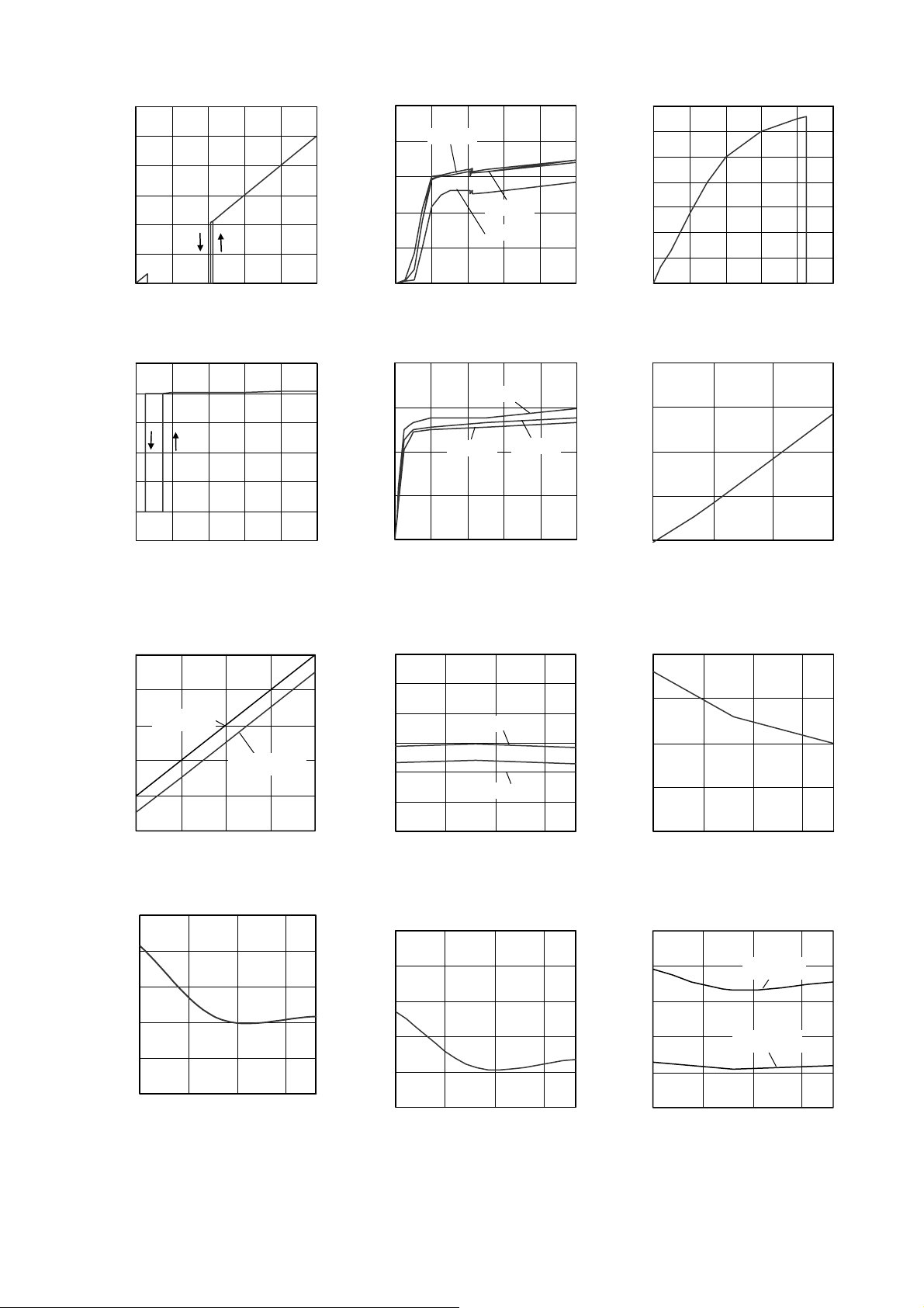
●Reference data (Unless otherwise specified, Ta = 25°C) : 4.1V Detection
リセット
時間
監視時間
リセット
時間
12
10
8
6
4
2
OUTPUT VOLTAGE: VOUT [V]
0
0246810
SUPPLY VOLTAGE: VDD [V]
Fig. 1 Detection Voltage
2
1.5
1
0.5
0
-0.5
CTW PIN CURRENT: ICTW [µA]
-1
012345
CTW PI N VOLTAGE: VC TW [V]
Fig. 4 CTW Charge Discharge Current
10
8
6
4
2
CIRCUIT CURRENT: IDD [µA]
0
0246810
SUPPLY VOLTAGE: VD D [ V]
Fig. 2 Total Supply Current
2
1.5
1
0.5
RESET CURRENT: IRESET [mA]
0
02 46 810
RESET VOLTAGE: VRESET [V]
Fig. 5 Output Current
Ta=105°C
Ta= −40°C
10000
1000
100
Monitor time
10
Reset time
1
WDT RESET TIME: Tw [ms]
0.1
0.001 0.01 0.1 1 10
CTW PIN CAPACITY : CTW[µF]
CT PIN VOLTAGE: VCT [V]
Fig. 7 WDT Time vs Capacitance
13
12
11
10
9
OUTPUT DELAY RESISTANCE: Rrst [MΩ]
8
-40 0 40 80
AMBIENT TEMPERATURE: Ta [℃]
Fig. 10 CT Pin Circuit Resistance vs
Temperature
5
4.75
4.5
4.25
4
3.75
DETECTION VOLTAGE: VDET [V]
3.5
-40 0 40 80
AMBIENT TEMPER ATURE: Ta [℃]
Fig. 8 Detection Voltage vs Temperature
10
9
8
7
6
OUTPUT DELAY TIME: TPLH [ms]
5
-40 0 40 80
AMBIENT TEMPERATURE: Ta [℃]
Fig. 11 RESET Transmission Delay
Time vs Temperature
Ta= 2 5° C
Ta= −40°C
Ta=105°C
L→H
H→L
Ta= 2 5° C
1400
1200
1000
800
600
400
200
CT PIN CURRENT: ICT [µA]
0
012345
CT PIN VOLTAGE: VCT [V]
Fig. 3 Delay Pin Current vs
10000
1000
100
10
OUTPUT DELAY TIME: TPLH [ms]
1
0.0001 0.001 0.01 0.1
Fig. 6 RESET Transmission Delay
1
0.75
0.5
0.25
OPERATING VOLTAGE: VOPL [V]
0
-40 0 40 80
AMBIENT TEMPER ATURE: Ta [℃]
Fig. 9 Operating Marginal Voltage vs
15
12
9
6
3
WDT RESET TIME: Tw [ms]
0
-40 0 40 80
AMBIENT TEMPER ATURE: Ta [℃]
Fig. 12 WDT Time vs Temperature
Power Supply Voltage
CT PIN CAPACITY: CT [µF]
Time vs Capacitance
Temperature
Monitor time
Reset time
3/8

●Block diagram
BD37A□□FVM BD87A□□FVM/BD99A41F
CLK
1
CT
2
Pulse
generation
circuit
CTW
3
Vref
R
Q
S
+
+
VDD
4
VthH
VthL
VDD
VDD
R
Q
S
+
8
7
GND
6
5
RESET
INH
N.C.
CTW
1
R
Q
S
+
CT
CLK
GND
2
3
Pulse
generation
circuit
4
Vref
VthH
VDD
+
+
VthL
CT pin capacitor: 470 pF to 3.3 µF
CTW pin capacitor: 0.001 µF to 10 µF
Fig.13
●Pin assignments
BD37A□□FVM BD87A□□FVM/BD99A41F
No.
Pin
name
Function
1 CLK Clock input from microcontroller
8765
1234
Fig.14
No.
Pin
name
Function
1 CTW WDT time setting capacitor connection pin
VDD
RESET
8
N.C.
7
R
Q
S
6
5
INH
VDD
2 CT Reset delay time setting capacitor connection pin
3 CTW WDT time setting capacitor connection pin
4 VDD Power supply pin
5 N.C. NC pin
6 GND GND pin
7 INH
WDT on/off setting pin
INH=H/L:WDT=ON/OFF
8 RESET Reset output pin
2 CT Reset delay time setting capacitor connection pin
3 CLK Clock input from microcontroller
4 GND GND pin
5 VDD Power supply pin
WDT on/off setting pin
6 INH
INH=H/L:WDT=OFF/ON(BD87A□□FVM)
INH=H/L:WDT=ON/OFF(BD99A41F)
7 N.C. NC pin
8 RESET Reset output pin
4/8

●I/O Circuit diagram
K
CT
VDD
VDD
INH
CT
VDD VDD
CLK
INH
CT
10MΩ(Typ.)
CTW
VDDVDD
CTW
RESET
RESET
Fig.15
●Timing chart
(BD37A□□FVM/BD99A41F)
VDD
INH
(BD87A□□FVM)
INH
VDETH
VDET
0
0
0
WDT circuit turns off
when INH is low.
WDT circuit turns off
when INH is high.
VDETH = VDET + Vrhys
CL
0
*4 TWCLK
TWCLK
VCT
VCTW
RESET
VCTH
0
0
0
VthH
VthL
(1) (2) (3)
TPLH
*2
*1
TWH
(5) (4)
*3
TWL
(6)(5)
(7) (7) (4)
(8)
(5)
(4)
(9)
(5)
(2)
(3)
(10)
(2)
(5)
(4)
(3)
(10)
(11) (10)
(4) (5) (4)
Fig.16
●Explanation
(1) The RESET pin voltage (RESET) switches to low when the power supply voltage (VDD) falls to 0.8 V.
(2) The external capacitor connected to the CT pin begins to charge when VDD rises above the reset detection voltage (VDETH). The
RESET signal stays low until VDD reaches the VDETH voltage and switches to high when VDD reaches or exceeds the VDETH voltage.
The RESET transmission delay time TPLH allowed to elapse before RESET switches from low to high is given by the following equation:
TPLH (s) ≈ 0.69 × Rrst × CT (µF) [1]
Rrst denotes the IC's built-in resistance and is designed to be 10 MΩ (Typ.). CT denotes the external capacitor connected to the CT pin.
(3) The external capacitor connected to the CTW pin begins to charge when RESET rises, triggering the watchdog timer.
(4) The CTW pin state switches from charge to discharge when the CTW pin voltage (VCTW) reaches VthH, and RESET switches from high
to low. The watchdog timer monitor time TWH is given by the following equation:
TWH (s) ≈ (0.5 × CTW (µF))/(ICTWC) [2]
ICTWC denotes the CTW charge current and is designed to be 0.50 µA (Typ.). CTW denotes the external capacitor connected to the
CTW pin.
5/8

(5) The CTW pin state switches from charge to discharge when VCTW reaches VthL, and RESET switches from low to high. The watchdog
G
timer reset time TWL is given by the following equation:
TWL (s) ≈ (0.5 × CTW (µF))/(ICTWO) [3]
ICTWO denotes the CTW discharge current and is designed to be 1.50 µA (Typ.).
(6) The CTW pin state may not switch from charge to discharge when the CLK input pulse width TWCLK is short. Use a TWCLK input pulse
width of at least 500 ns.
TWCLK ≥ 500 ns (Min.)
(7) When a pulse (positive edge trigger) of at least 500 ns is input to the CLK pin while the CTW pin is charging, the CTW state switches from
charge to discharge. Once it discharges to VthL, it will charge again.
(8) Watchdog timer operation is forced off when the INH pin switches to low:BD37A□□FVM (Switches to high:BD87A□□FVM,BD97A41F).
At that time, only the watchdog timer is turned off. Reset detection is performed normally.
(9) The watchdog timer function turns on when the INH pin switches to high. The external capacitor connected to the CTW pin begins to
charge at that time.
(10) RESET switches from high to low when VDD falls to the RESET detection voltage (VDET) or lower.
(11) When VDD falls to 0 V, the RESET signal stays low until VDD reaches 0.8 V.
●Heat reduction curve
800
When mounted on a glass epoxy board
(70 mm
600
470mW
400
MSOP8 SOP8
800
When mounted on a glass epoxy board
(70 mm
× 70 mm × 1.6mm) θja = 212.8 (°C /W)
600
550mW
400
× 70 mm × 1.6mm) θja = 181.8 (°C /W)
200
105
POWER DISSIPATION: Pd [mW]
0
25 50 75 125100
AMBIENT TEMPERATURE: Ta [℃]
℃
200
105
POWER DISSIPATION: Pd [mW]
0
0
25 50 75 125100
AMBIENT TEMPERATURE: Ta [℃]
℃
Fig.17
●External settings for pins and precautions
1) Connect a capacitor (0.001 µF to 1,000 µF) between the VDD and GND pins when the power line impedance is high. Use of the IC when
the power line impedance is high may result in oscillation.
2) External capacitance
A capacitor must be connected to the CTW pin. When using a large capacitor such as 1 µF, the INH pin must allow a CTW discharge time of
at least 2 ms. The power-on reset time is given by equation [1] on page 5. The WDT time is given by equations [2] and [3] on page 5, 6. The
setting times are proportional to the capacitance value from the equations, so the maximum and minimum setting times can be calculated
from the electrical characteristics according to the capacitance. Note however that the electrical characteristics do not include the external
capacitor's temperature characteristics.
●Operation Notes
1. Absolute maximum ratings
An excess in the absolute maximum ratings, such as supply voltage, temperature range of operating conditions, etc., can break down the
devices, thus making impossible to identify breaking mode, such as a short circuit or an open circuit. If any over rated values will expect to
exceed the absolute maximum ratings, consider adding circuit protection devices, such as fuses.
2. GND voltage
The potential of GND pin must be minimum potential in all operating conditions.
Thermal design
3.
Use a thermal design that allows for a sufficient margin in light of the power dissipation (Pd) in actual operating conditions.
Inter-pin shorts and mounting errors
4.
Use caution when positioning the IC for mounting on printed circuit boards. The IC may be damaged if there is any connection error or if pins
are shorted together.
6/8

5. Actions in strong electromagnetic field
Use caution when using the IC in the presence of a strong electromagnetic field as doing so may cause the IC to malfunction.
Testing on application boards
6.
When testing the IC on an application board, connecting a capacitor to a pin with low impedance subjects the IC to stress. Always discharge
capacitors after each process or step. Always turn the IC's power supply off before connecting it to or removing it from a jig or fixture during
the inspection process. Ground the IC during assembly steps as an antistatic measure. Use similar precaution when transporting or storing
the IC.
Regarding input pin of the IC
7.
This monolithic IC contains P+ isolation and P substrate layers between adjacent elements in order to keep them isolated.
P-N junctions are formed at the intersection of these P layers with the N layers of other elements, creating a parasitic diode or transistor. For
example, the relation between each potential is as follows:
When GND > Pin A and GND > Pin B, the P-N junction operates as a parasitic diode.
When GND > Pin B, the P-N junction operates as a parasitic transistor.
Parasitic diodes can occur inevitable in the structure of the IC. The operation of parasitic diodes can result in mutual interference among
circuits, operational faults, or physical damage. Accordingly, methods by which parasitic diodes operate, such as applying a voltage that is
lower than the GND (P substrate) voltage to an input pin, should not be used.
(Pin A)
Resistor
(Pin B)
Transistor (NPN)
C
B
E
(Pin B)
C
B
N N
P
Ground Wiring Pattern
8.
P
N
GND
P+ P+
Parasitic element
P+
N N
Parasitic element
or transistor
P
N
P substrate
GND
Fig. 18 Example of IC structure
P+
(Pin A)
E
GND
Parasitic element or
transistor
Parasitic element
When using both small signal and large current GND patterns, it is recommended to isolate the two ground patterns, placing a single ground
point at the ground potential of application so that the pattern wiring resistance and voltage variations caused by large currents do not cause
variations in the small signal ground voltage. Be careful not to change the GND wiring pattern of any external components, either.
9. Applications or inspection processes with modes where the potentials of the VDD pin and other pins may be reversed from their normal states
may cause damage to the IC’s internal circuitry or elements. Use an output pin capacitance of 1000µF or lower in case VDD is shorted with the
GND pin while the external capacitor is charged. It is recommended to insert a diode for preventing back current flow in series with VDD or
bypass diodes between Vcc and each pin.
Back current prevention diode
Bypass diode
VDD
Pin
Fig.19
When VDD falls below the operating marginal voltage, output will be open. When output is being pulled up to input, output will be equivalent
10.
to VDD.
Input pin
11.
The CLK and INH pins comprise inverter gates and should not be left open. (These pins should be either pulled up or down.) Input to the CLK
pin is detected using a positive edge trigger and does not affect the CLK signal duty. Input the trigger to the CLK pin within the TWH time.
7/8

●Selecting a model name when ordering
A
y
y
(
B D 3
7
ROHM model
name
MSOP8
<Dimension>
Part number
37A: H Active
87A: L Active
99A: H Active
4.0 ± 0.2
0.475
0.9Max.
0.75 ± 0.05
2.9 ± 0.1
0.1
±
2.8
0.65
0.08 ± 0.05
58
0.6 ± 0.2
0.29 ± 0.15
41
0.22
+0.05
−0.04
0.08 S
0.145
+0.05
−0.03
0.08
M
4
Detection
voltage
F 1
Package type
FVM : MSOP8
<Tape and Reel information>
Tape
Quantit
Direction
of feed
Embossed carrier tape
TR
(The direction is the 1pin of product is at the upper light when you
hold
reel on the left hand and you pull out the tape on the right hand)
V
F : SOP8
M
T R
Taping
E2: Reel-wound embossed taping
TR: Reel-wound embossed taping
SOP8
<Dimension>
5.0±0.2
85
4.4±0.2
6.2±0.3
1.27
0.11
1.5±0.1
0.4±0.1
0.3Min.
41
0.15±0.1
0.1
(Unit:mm)
<Tape and Reel information>
Tape
Quantit
Direction
of feed
Unit:mm
Reel
※When you order , please order in times the amount of package quantity.
Embossed carrier tape
2500pcs
E2
(The direction is the 1pin of product is at the upper left when you hold
reel on the left hand and you pull out the tape on the right hand)
1234
1234
Reel
※When you order , please order in times the amount of package quantity.
1234
1Pin
1234
1Pin
Direction of
1234
1234
Direction of feed
1234
1234
Catalog No.05T391Be '06.7 ROHM C 1000 TSU
Appendix
Notes
No technical content pages of this document may be reproduced in any form or transmitted by any
means without prior permission of ROHM CO.,LTD.
The contents described herein are subject to change without notice. The specifications for the
product described in this document are for reference only. Upon actual use, therefore, please request
that specifications to be separately delivered.
Application circuit diagrams and circuit constants contained herein are shown as examples of standard
use and operation. Please pay careful attention to the peripheral conditions when designing circuits
and deciding upon circuit constants in the set.
Any data, including, but not limited to application circuit diagrams information, described herein
are intended only as illustrations of such devices and not as the specifications for such devices. ROHM
CO.,LTD. disclaims any warranty that any use of such devices shall be free from infringement of any
third party's intellectual property rights or other proprietary rights, and further, assumes no liability of
whatsoever nature in the event of any such infringement, or arising from or connected with or related
to the use of such devices.
Upon the sale of any such devices, other than for buyer's right to use such devices itself, resell or
otherwise dispose of the same, no express or implied right or license to practice or commercially
exploit any intellectual property rights or other proprietary rights owned or controlled by
ROHM CO., LTD. is granted to any such buyer.
Products listed in this document are no antiradiation design.
The products listed in this document are designed to be used with ordinary electronic equipment or devices
(such as audio visual equipment, office-automation equipment, communications devices, electrical
appliances and electronic toys).
Should you intend to use these products with equipment or devices which require an extremely high level
of reliability and the malfunction of which would directly endanger human life (such as medical
instruments, transportation equipment, aerospace machinery, nuclear-reactor controllers, fuel controllers
and other safety devices), please be sure to consult with our sales representative in advance.
It is our top priority to supply products with the utmost quality and reliability. However, there is always a chance
of failure due to unexpected factors. Therefore, please take into account the derating characteristics and allow
for sufficient safety features, such as extra margin, anti-flammability, and fail-safe measures when designing in
order to prevent possible accidents that may result in bodily harm or fire caused by component failure. ROHM
cannot be held responsible for any damages arising from the use of the products under conditions out of the
range of the specifications or due to non-compliance with the NOTES specified in this catalog.
Thank you for your accessing to ROHM product informations.
More detail product informations and catalogs are available, please contact your nearest sales office.
ROHM Customer Support System
www.rohm.com
THE AMERICAS / EUROPE / ASIA / JAPAN
Contact us : webmaster@ rohm.co. jp
Copyright © 2008 ROHM CO.,LTD.
21 Saiin Mizosaki-cho, Ukyo-ku, Kyoto 615-8585, Japan
Appendix1-Rev2.0
TEL : +81-75-311-2121
FAX : +81-75-315-0172
 Loading...