

Single-chip Type with Built-in FET Switching Regulators
Output 1.5A or Less
High-efficiency Step-down Switching Regulator
with Built-in Power MOSFET
BD8312HFN
●Description
BD8312HFN produces step-down output including 1.2, 1.8, 3.3, or 5 V from 4 batteries, batteries such as Li2cell or Li3cell,
etc. or a 5V/12V fixed power supply line.
This IC allows easy production of small power supply by a wide range of external constants, and is equipped with an external
coil/capacitor downsized by high frequency operation of 1.5 MHz, built-in synchronous rectification SW capable of
withstanding 15 V, and flexible phase compensation system on board.
●Features
1) Incorporates Pch/Nch synchronous rectification SW capable of withstanding 1.0 A/15V.
2) Incorporates phase compensation device between input and output of Error AMP.
3) Small coils and capacitors to be used by high frequency operation of 1.5MHz
4) Input voltage 3.5 V – 14 V
Output current 1.2A(7.4V input, 3.3V output)
0.8A(4.5V input, 3.3V output)
5) Incorporates soft-start function.
6) Incorporates timer latch system short protecting function.
7) As small as 2.9mm×3 mm, SON 8-pin package HSON8
●Application
For portable equipment like DSC/DVC powered by 4 dry batteries or Li2cell and Li3cell, or general consumer-equipment
with 5 V/12 V lines
●Operating Conditions (Ta = 25℃)
Parameter Symbol Voltage circuit Unit
Power supply voltage VCC 3.5 to 14 V
Output voltage VOUT 1.2 to 12 V
●Absolute Maximum Ratings
Parameter Symbol Rating Unit
Maximum applied power voltage VCC, PVCC 15 V
Maximum input current Iinmax 1.0 A
Power dissipation Pd 630 mW
Operating temperature range Topr -25 to +85 ℃
Storage temperature range Tstg -55 to +150 ℃
Junction temperature Tjmax +150 ℃
*1 When used at Ta = 25℃ or more installed on a 70×70×1.6tmm board, the rating is reduced by 5.04mW/℃.
* These specifications are subject to change without advance notice for modifications and other reasons.
No.11027EDT04
www.rohm.com
© 2011 ROHM Co., Ltd. All rights reserved.
1/14
2011.04 - Rev.D

BD8312HFN
Technical Note
●Electrical Characteristics
(Unless otherwise specified, Ta = 25 ℃, VCC = 7.4 V)
Parameter Symbol
Target Value
Min Typ Max
Unit Conditions
[Low voltage input malfunction preventing circuit]
Detection threshold voltage VUV - 2.9 3.2 V VREG monitor
Hysteresis range ΔVUVhy 100 200 300 mV
[Oscillator]
Oscillation frequency Fosc 1.38 1.5 1.62 MHz
[Regulator]
Output voltage VREG 4.65 5.0 5.35 V
[Error AMP]
INV threshold voltage VINV 0.99 1.00 1.01 V
Input bias current IINV -50 0 50 nA VCC=12.0V , VINV=6.0V
Soft-start time Tss 3.2 5.3 7.4 msec
[PWM comparator]
LX Max Duty Dmax - - (※)100 %
[Output]
PMOS ON resistance RONP - 450 600 mΩ
NMOS ON resistance RONN - 300 420 mΩ
Leak current Ileak -1 0 1 µA
[STB]
STB pin
control voltage
STB pin pull-down resistance
Operation VSTBH 2.5 - 11 V
No-operation VSTBL -0.3 - 0.3 V
250 400 700 kΩ
[Circuit current]
Standby current
VCC pin I
PVCC pin ISTB2 - - 1 µA
Circuit current at operation VCC
Circuit current at operation PVCC
(※1) 100% is MAX Duty as behavior of a PWM conparetor.
Using in region where High side PMOS is 100% on state when the same or less input voltage than output voltage is supplied as an application circuit
causes detection of SCP then DC/DC converter stops.
Not designed to be resistant to radiation
STB1 - - 1 µA
- 600 900 µA VINV=1.2V
- 30 50 µA VINV=1.2V
www.rohm.com
© 2011 ROHM Co., Ltd. All rights reserved.
2/14
2011.04 - Rev.D
BD8312HFN
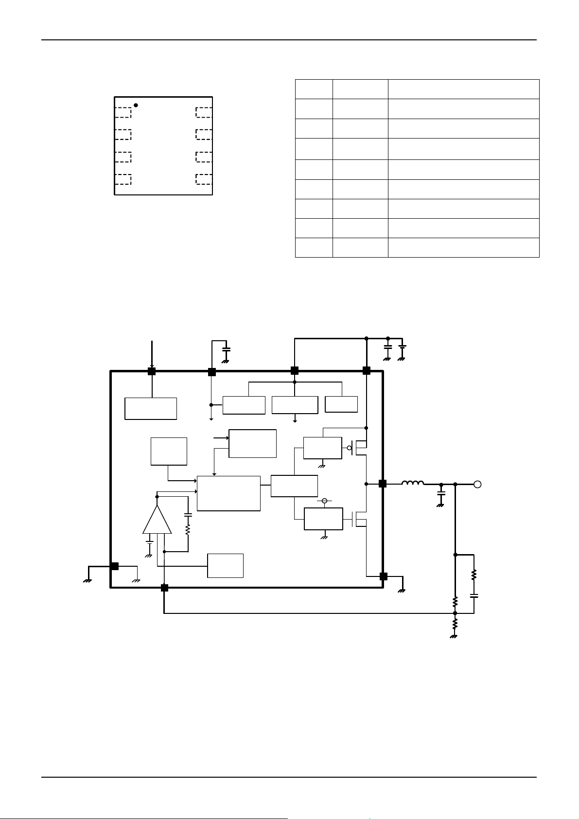
●Description of Pins
GND
VCC
VREG
INV
STB
PVCC
PGND
Lx
Fig.1 Terminal layout
Pin No. Pin Name Function
1 GND Ground terminal
2 VCC Control part power input terminal
3 VREG
4 PGND Power transistor ground terminal
5 Lx Coil connecting terminal
6 PVCC DC/DC converter input terminal
7 STB ON/OFF terminal
8 INV Error AMP input terminal
●Block Diagram
ON/OFF
STB
VREG
VCC
STBY_IO
1.0MHz
OSC
DC/DC
converter
100% High
Duty
STOP
5V REG
SCP
OSC×4000 count
PWM
CONTROL
Step down
GND
VREF
+-+
ERROR_AMP
Soft
Start
OSC×8000 count
INV
Reference
VREF
PRE
DRIVER
TIMMING
CONTROL
PRE
DRIVER
Fig.2 Block diagram
Technical Note
5 V output terminal of regulator for
internal circuit
PVCC
UVLO
450mΩ
LX
VREG
300mΩ
PGND
www.rohm.com
© 2011 ROHM Co., Ltd. All rights reserved.
3/14
2011.04 - Rev.D

BD8312HFN
●Description of Blocks
1. Reference
This block produces ERROR AMP standard voltage.
The standard voltage is 1.0 V.
2. 5 V Reg
5 V low saturation regulator for internal analog circuit
BD8312HFN is equipped with this regulator for the purpose of protecting the internal circuit from high voltage. Therefore,
this output is reduced when VCC is less than 5 V, then PMOS ON resistance increases and Power efficiency and
Maximum output current of DC/DC converter decreases in this region. Please see attached data (fig14,15,16,17) about
increasing of PMOS ON resistance in this region.
3 UVLO
Circuit for preventing low voltage malfunction
Prevents malfunction of the internal circuit at activation of the power supply voltage or at low power supply voltage.
Monitors VCC pin voltage to turn off all output FET and DC/DC converter output when VCC voltage is lower than 2.9 V,
and reset the timer latch of the internal SCP circuit and soft-start circuit. This threshold contains 200 mV hysteresis.
4 SCP
Timer latch system short-circuit protection circuit
When DC/DC converter is 100% High Duty , the internal SCP circuit starts counting.
The internal counter is in synch with OSC, the latch circuit is activated about 2.7 msec after the counter counts about 4000
oscillations to turn off DC/DC converter output.
To reset the latch circuit, turn off the STB pin once. Then, turn it on again or turn on the power supply voltage again.
5 OSC
Circuit for oscillating sawtooth waves with an operation frequency fixed at 1.5 MHz
6 ERROR AMP
Error amplifier for detecting output signals and output PWM control signals
The internal standard voltage is set at 1.0 V.
A primary phase compensation device of 200 pF, 62 kΩ is built in-between the inverting input terminal and the output
terminal of this ERROR AMP.
7 PWM COMP
Voltage-pulse width converter for controlling output voltage corresponding to input voltage
Comparing the internal SLOPE waveform with the ERROR AMP output voltage, PWM COMP
controls the pulse width to the output to the driver.
8 SOFT START
Circuit for preventing in-rush current at startup by bringing the output voltage of the DC/DC converter into a soft-start
Soft-start time is in synch with the internal OSC, and the output voltage of the DC/DC converter reaches the set voltage
after about 8000 oscillations.
9 PRE DRIVER/TIMING CONTROL
CMOS inverter circuit for driving the built-in synchronous rectification SW
The synchronous rectification OFF time for preventing feedthrough is about 25 nsec.
10 STBY_IO
Voltage applied on STB pin (7 pin) to control ON/OFF of IC
Turned ON when a voltage of 2.5 V or higher is applied and turned OFF when the terminal is open or 0 V is applied.
Incorporates approximately 400 kΩ pull-down resistance.
11 Pch/Nch FET SW
Built-in synchronous rectification SW for switching the coil current of the DC/DC converter
Incorporates a 450 mΩ PchFET SW capable of withstanding 15 V.and 300 mΩ SW capable of withstanding 15 V.
Since the current rating of this FET is 1.0A, it should be used within 1.0A including the DC current and ripple current of the coil.
Technical Note
www.rohm.com
© 2011 ROHM Co., Ltd. All rights reserved.
4/14
2011.04 - Rev.D

BD8312HFN
●Reference data
(Unless otherwise specified, Ta = 25℃, VCC = 7.4 V)
1.02
1.02
1.01
1.01
1.00
INV THRESHOLD [V]
0.99
1.00
INV THRESHOLD [V]
0.99
0.98
-40 -20 0 20 40 60 80 100 120
TEMPERATURE [℃]
0.98
Fig.3. INV
8
7
6
5
4
VREG[V]
3
2
1
0
02468101214
VCC [V]
1.7
1.6
1.5
FREQUENCY [MHz]
1.4
1.3
Fig.6. VREG
3.50
Hysteresis width
3.30
Vhys [V]
3.10
UVLO release voltage
0.25
0.20
0.15
02468101214
VCC [V]
Fig.4. INV
-40 0 40 80 120
TEMPERATURE [℃]
Fig.7. fosc
500
ID=500mA
400
300
Technical Note
5.3
5.2
5.1
5.0
4.9
VREG VOLTAGE [V]
4.8
4.7
-40 0 40 80 120
TEMPERATURE [℃]
Fig.5. VREG output
1.7
1.6
1.5
FREQUENCY [ MHz ]
1.4
1.3
3691215
600
ID=500mA
500
400
300
VCC [V]
Fig.8. fosc
2.90
ヒステリシス電圧
2.70
Hysteresis Voltage Vhys[V]
UVLO detection voltage
2.50
-40 0 40 80 120
Environmental temperature Ta [°C]
環境温度
Ta [℃]
Fig.9. UVLO
www.rohm.com
© 2011 ROHM Co., Ltd. All rights reserved.
0.10
0.05
0.00
200
ON RESISTANCE [ mΩ ]
100
-40 0 40 80 120
TEMPARATURE [℃]
Fig.10. Nch FET ON resistance
5/14
200
ON RESISTANCE [ mΩ]
100
0
3 6 9 12 15
VCC [V]
Fig.11. Nch FET ON resistance
2011.04 - Rev.D

BD8312HFN
800
ID=500mA
600
400
200
SWOUT ON Resistance [Ω ]
0
-40 0 40 80 120
TEMPARATURE [℃]
Fig.12. Pch FET ON resistance
temperature property
3.0
2.5
2.0
Ta= 8 5℃
1.5
1.0
PMOS ON Resistance (Ω)
0.5
0.0
0.0 1.0 2.0
Fig.15.PchFET ON resistance
Io property [VCC=4.0V]
Io [A]
Ta= 2 5℃
Ta= - 25 ℃
1000
ID=500mA
800
600
400
200
SWOUT ON Resistance [Ω ]
0
3691215
VCC [V]
Fig.13. Pch FET ON resistance
power supply property
3.0
2.5
2.0
1.5
1.0
PMOS ON Resistance (Ω)
0.5
0.0
0.0 1.0 2.0
Ta= 8 5℃ Ta= 8 5℃
Ta= 2 5℃
Ta= - 25 ℃
Io [A]
Fig.16.PchFET ON resistance
Io property [VCC=4.5V]
Technical Note
3.0
Ta= 8 5℃
2.5
2.0
1.5
1.0
PMOS ON Resistance (Ω)
0.5
0.0
0.0 1.0 2.0
Fig.14.PchFET ON resistance
Io property [VCC=3.5V]
3.0
2.5
2.0
1.5
1.0
PMOS ON Resistance (Ω)
0.5
0.0
0.0 1.0 2.0
Fig.17.PchFET ON resistance
Io property [VCC=5.0V]
Ta= 2 5℃
Ta= - 25 ℃
Io [A]
Ta= 2 5℃
Ta= - 25 ℃
Io [A]
2.5
2.0
1.5
STB Voltage [V]
1.0
-50 0 50 100 150
ON
OFF
Ta [℃]
Fig.18. STB
www.rohm.com
© 2011 ROHM Co., Ltd. All rights reserved.
1000
800
600
400
ICC [uA]
200
0
-40 0 40 80 120
TEMPARATURE [℃]
Fig.19. Circuit current
temperature property
6/14
1000
800
600
ICC [uA]
400
200
0
02468101214
VCC [V]
Fig.20. Circuit current
2011.04 - Rev.D

BD8312HFN
●Example of Application Input: 4.5 to 10 V, output: 3.3 V / 500mA
VBAT=4.5~10V
1μF
GRM188B11A105KA61
(Murata)
GND
Technical Note
INV
1μF
GRM188B11A105KA61
(Murata)
●Reference application data 1
100
80
VCC=4.5V
60
40
EFFICIENCY [%]
20
VCC=5.5V
VCC=7.5V
VCC
VREG
PGND
STB
PVCC
Lx
Fig.21 Reference application diagram
3.35
3.33
3.31
3.29
OUTPUT VOLTAGE [V]
3.27
VCC=7.5V
VCC=4.5V
ON/OFF
4.7μH
1098AS-4R7M(TOKO)
VCC=5.5V
3.3V/500mA
10μF
GRM31CB11A106KA01
(Murata)
10kΩ
10pF
200kΩ
51kΩ
22kΩ
0
1 10 100 1000
OUTPUT CURRENT [mA]
Fig.22 Power conversion efficiency
(VOUT = 3.3 V)
www.rohm.com
© 2011 ROHM Co., Ltd. All rights reserved.
3.25
1 10 100 1000
OUTPUT CURRENT [m A]
Fig.23 Load regulation
(VOUT = 3.3 V)
7/14
2011.04 - Rev.D

BD8312HFN
●Reference application data 2 (Input 4.5 V, 6.0 V, 8.4 V, 10 V, output 3.3 V )
Technical Note
60
40
20
0
Gain [dB]
-20
-40
-60
100 1000 10000 100000 1000000
Gain
[Hz]
周波数
Frequency [Hz]
Fig.24 Frequency response 1
=
60
40
20
0
Gain [dB]
-20
-40
=
Gain
-60
100 1000 10000 100000 1000000
Frequency [Hz]
周波数
[Hz]
Fig.27 Frequency response 4
=
=
Phase
Phase
180
120
60
0
-60
-120
-180
180
120
60
0
-60
-120
-180
60
40
20
0
Gain [dB]
Phase [deg]
-20
-40
-60
100 1000 10000 100000 1000000
Gain
[Hz]
Frequency [Hz] Frequency [Hz]
周波数
Fig.25 Frequency response 2
=
60
40
20
0
Gain [dB]
Phase [deg]
-20
-40
-60
100 1000 10000 100000 1000000
Frequency [Hz] Frequency [Hz]
[Hz]
周波数
Fig.28 Frequency response 5
=
Gain
=
=
Phase
Phase
180
120
60
0
-60
-120
-180
180
120
60
0
-60
-120
-180
60
40
20
0
Gain [dB]
Phase [deg]
-20
-40
-60
100 1000 10000 100000 1000000
周波数
Fig.26 Frequency response 3
=
60
40
20
0
Gain [dB]
Phase [deg]
-20
-40
-60
100 1000 10000 100000 1000000
Gain
周波数
Fig.29 Frequency response 6
=
[Hz]
[Hz]
Gain
=
Phase
=
Phase
180
120
60
0
-60
-120
-180
180
120
60
0
-60
-120
-180
Phase [deg]
Phase [deg]
60
40
20
0
Gain [dB]
-20
-40
-60
100 1000 10000 100000 1000000
Frequency [Hz]
周波数
Phase
Gain
[Hz]
Fig.30 Frequency response 7
=
=
180
120
60
0
-60
-120
-180
60
40
20
0
Gain [dB]
Phase [deg]
-20
-40
-60
100 1000 10000 100000 1000000
Frequency [Hz]
周波数
Fig.31 Frequency response 8
=
Gain
[Hz]
=
Phase
180
120
60
0
-60
-120
-180
Phase [deg]
www.rohm.com
© 2011 ROHM Co., Ltd. All rights reserved.
8/14
2011.04 - Rev.D

BD8312HFN
Technical Note
●Reference board pattern
VOUT
VBAT
Lx
GND
・The radiation plate on the rear should be a GND flat surface of low impedance in common with the PGND flat surface.
・It is recommended to install a GND pin in another system as shown in the drawing without connecting it directly to this PNGD.
・Produce as wide a pattern as possible for the VBAT, Lx and PGND lines in which large current flows.
●Selection of Part for Applications
(1) Inductor
A shielded inductor that satisfies the current rating (current value,
Ipecac as shown in the drawing below) and has a low DCR
(direct resistance component) is recommended.
ΔIL
Inductor values affect inductor ripple current, which will cause output
ripple.
Ripple current can be reduced as the coil L value becomes larger
and the switching frequency becomes higher.
Fig.32 Inductor current
Ipeak =Iout + ⊿IL/2 [A] (1)
Vin-Vout
⊿IL= × × [A] (2)
L
Vout
Vin
1
f
(η: Efficiency, ⊿IL: Output ripple current, f: Switching frequency)
As a guide, inductor ripple current should be set at about 20 to 50% of the maximum input current.
*Current over the coil rating flowing in the coil brings the coil into magnetic saturation, which may lead to lower efficiency
or output oscillation. Select an inductor with an adequate margin so that the peak current does not exceed the rated
current of the coil.
(2) Output capacitor
A ceramic capacitor with low ESR is recommended for output in order to reduce output ripple.
There must be an adequate margin between the maximum rating and output voltage of the capacitor, taking the DC bias
property into consideration.
Output ripple voltage is acquired by the following equation.
Vpp=⊿IL× + ⊿IL×R
1
ESR
2π×f×Co
[V] ・・・ (3)
Setting must be performed so that output ripple is within the allowable ripple voltage.
www.rohm.com
© 2011 ROHM Co., Ltd. All rights reserved.
9/14
2011.04 - Rev.D

BD8312HFN
Technical Note
(3) Output voltage setting
The internal standard voltage of the ERROR AMP is 1.0 V. Output voltage is acquired by Equation (4).
VOUT
R1
R2
INV
ERROR AMP
(R1+R2)
Vo= ×1.0 [V] ・・・ (4)
R2
VREF
1.0 V
Fig.33 Setting of voltage feedback resistance
(4) DC/DC converter frequency response adjustment system
Condition for stable application
The condition for feedback system stability under negative feedback is that the phase delay is 135 °or less when gain is 1
(0dB).
Since DC/DC converter application is sampled according to the switching frequency, the bandwidth GBW of the whole
system (frequency at which gain is 0 dB) must be controlled to be equal to or lower than 1/10 of the switching frequency.
In summary, the conditions necessary for the DC/DC converter are:
- Phase delay must be 135°or lower when gain is 1 (0 dB).
- Bandwidth GBW (frequency when gain is 0 dB) must be equal to or lower than 1/10 of the switching frequency.
To satisfy those two points, R
, R2, R3, DS and RS in Fig. 34 should be set as follows.
1
, R2, R3
[1] R
1
BD8313HFN incorporates phase compensation devices of
R4=62kΩ and C2=200pF. These C2 and R
, R2, and R
1
3
valuesdecide the primary pole that determines the bandwidth
of DC/DC converter.
VOUT
R1
Cs
Rs
Inside of IC
R4
Primary pole point frequency
DC/DC converter DC Gain
fp=
2π A×( +R
DC Gain =A× ×
R
1×R2
R1+R
1
B
1
)×C2
3
2
V
IN
VO
R2
・・・・(1)
Fig.34 Example of phase compensation setting
・・・・(2)
R3
A: Error AMP Gain
About 100dB = 10
B: Oscillator amplification = 0.5
V
IN:
V
OUT
Input voltage
: Output voltage
By Equations (1) and (2), the frequency fsw of point 0 dB under limitation of the bandwidth of the DC gain at the primary
pole point is as shown below.
f
= fp×DC Gain = × ×
SW
2πC2×( +R3 )
1
(R
R2)
1
・
(R1+R2)
1
B
VIN
VO
・・・・(3)
It is recommended that fsw should be approx.10 kHz. When load response is difficult, it may be set at approx. 20 kHz.
By Equation (3), R
and R2, which determine the voltage value, will be in the order of several hundred kΩ. If an
1
appropriate resistance value is not available since the resistance is so high and routing may cause noise, the use of R
enables easy setting.
C2
5
FB
3
www.rohm.com
© 2011 ROHM Co., Ltd. All rights reserved.
10/14
2011.04 - Rev.D

BD8312HFN
Technical Note
[2] Cs and Rs setting
For DC/DC converter, the 2nd dimension pole point is caused by the coil and capacitor as expressed by the following
equation.
f
=
LC
1
2π√(LC)
・・・・(4)
This secondary pole causes a phase rotation of 180°. To secure the stability of the system, put a zero point in 2 places to
perform compensation.
Zero point by built-in CR f
Zero point by Cs f
Setting f
to be half to 2 times a frequency as large as f
Z2
= = 13kHz
Z1
=
Z1
1
・・・・(5)
2πR4C2
1
・・・・(6)
2π(R1+R3)CS
provides an appropriate phase margin.
LC
It is desirable to set Rs at about 1/20 of (R1+R3) to cancel any phase boosting at high frequencies.
Those pole points are summarized in the figure below. The actual frequency property is different from the ideal
calculation because of part constants. If possible, check the phase margin with a frequency analyzer or network analyzer.
Otherwise, check for the presence or absence of ringing by load response waveform and also check for the presence or
absence of oscillation under a load of an adequate margin.
(6)
(5)
(3)
(4)
Fig.35 Example of DC/DC converter frequency property
(Measured with FRA5097 by NF Corporation)
www.rohm.com
© 2011 ROHM Co., Ltd. All rights reserved.
11/14
2011.04 - Rev.D

BD8312HFN
Technical Note
●I/O Equivalence Circuit
STB INV
STB
VCC
INV
VREGVCC
Lx, PGND, PVCC
PVCC
Lx
VREG
VCC
VCC
VREG
PGND
www.rohm.com
© 2011 ROHM Co., Ltd. All rights reserved.
12/14
2011.04 - Rev.D

BD8312HFN
~
~
Technical Note
●Notes for use
1) Absolute Maximum Rating
We dedicate much attention to the quality control of these products, however the possibility of deterioration or destruction
exists if the impressed voltage, operating temperature range, etc., exceed the absolute maximum ratings. In addition, it is
impossible to predict all destructive situations such as short-circuit modes, open circuit modes, etc. If a special mode
exceeding the absolute maximum rating is expected, please review matters and provide physical safety means such as
fuses, etc.
2) GND Potential
Keep the potential of the GND pin below the minimum potential at all times.
3) Thermal Design
Work out the thermal design with sufficient margin taking power dissipation (Pd) in the actual operation condition into account.
4) Short Circuit between Pins and Incorrect Mounting
Attention to IC direction or displacement is required when installing the IC on a PCB. If the IC is installed in the wrong way,
it may break. Also, the threat of destruction from short-circuits exists if foreign matter invades between outputs or the
output and GND of the power supply.
5) Operation under Strong Electromagnetic Field
Be careful of possible malfunctions under strong electromagnetic fields.
6) Common Impedance
When providing a power supply and GND wirings, show sufficient consideration for lowering common impedance and
reducing ripple (i.e., using thick short wiring, cutting ripple down by LC, etc.) as much as you can.
7) Thermal Protection Circuit (TSD Circuit)
This IC contains a thermal protection circuit (TSD circuit). The TSD circuit serves to shut off the IC from thermal runaway
and does not aim to protect or assure operation of the IC itself. Therefore, do not use the TSD circuit for continuous use or
operation after the circuit has tripped.
8) Rush Current at the Time of Power Activation
Be careful of the power supply coupling capacity and the width of the power supply and GND pattern wiring and routing since
rush current flows instantaneously at the time of power activation in the case of CMOS IC or ICs with multiple power supplies.
9
) IC Terminal Input
This is a monolithic IC and has P+ isolation and a P substrate for element isolation between each element. P-N junctions
are formed and various parasitic elements are configured using these P layers and N layers of the individual elements.
For example, if a resistor and transistor are connected to a terminal as shown on Fig.36:
○ The P-N junction operates as a parasitic diode when GND > (Terminal A) in the case of a resistor or when GND >
(Pin B) in the case of a transistor (NPN)
○ Also, a parasitic NPN transistor operates using the N layer of another element adjacent to the previous diode in
the case of a transistor (NPN) when GND > (Pin B).
The parasitic element consequently rises under the potential relationship because of the IC’s structure. The parasitic
element pulls interference that could cause malfunctions or destruction out of the circuit. Therefore, use caution to avoid
the operation of parasitic elements caused by applying voltage to an input terminal lower than the GND (P board), etc.
(Pin A)
N
Resistor
N
P Substrate
P
+
P+
P
Parasitic Element
(Pin B)
N
N
Parasitic Element
Transistor (NPN)
C
+
P
P Substrate
B
E
GND
N
P
N
+
P
N
GND
(Pin A)
Parasitic Element
GND
Fig.36 Example of simple structure of Bipolar IC
~
~
www.rohm.com
© 2011 ROHM Co., Ltd. All rights reserved.
13/14
2011.04 - Rev.D

BD8312HFN
●Ordering part number
B D 8 3 1 2 H F N - T R
Part No. Part No.
HSON8
2.9± 0.1
(MAX 3.1 include BURR)
0.475
8765
2.8± 0.1
3.0± 0.2
0.6MAX
+0.03
0.02
–0.02
4312
1PIN MARK
0.65
S
0.32±0.1
(0.2)
(1.8)
(0.2)
0.1 S
0.08
(0.45)
(2.2)
54632718
M
(0.05)
(0.3)
(0.15)
+0.1
0.13
–0.05
(Unit : mm)
Package
HFN:HSON8
<Tape and Reel information>
Embossed carrier tapeTape
Quantity
Direction
of feed
3000pcs
TR
The direction is the 1pin of product is at the upper right when you hold
()
reel on the left hand and you pull out the tape on the right hand
Reel
Packaging and forming specification
TR: Embossed tape and reel
1pin
Order quantity needs to be multiple of the minimum quantity.
∗
Technical Note
Direction of feed
www.rohm.com
© 2011 ROHM Co., Ltd. All rights reserved.
14/14
2011.04 - Rev.D

Notes
No copying or reproduction of this document, in part or in whole, is permitted without the
consent of ROHM Co.,Ltd.
The content specied herein is subject to change for improvement without notice.
The content specied herein is for the purpose of introducing ROHM's products (hereinafter
"Products"). If you wish to use any such Product, please be sure to refer to the specications,
which can be obtained from ROHM upon request.
Examples of application circuits, circuit constants and any other information contained herein
illustrate the standard usage and operations of the Products. The peripheral conditions must
be taken into account when designing circuits for mass production.
Great care was taken in ensuring the accuracy of the information specied in this document.
However, should you incur any damage arising from any inaccuracy or misprint of such
information, ROHM shall bear no responsibility for such damage.
The technical information specied herein is intended only to show the typical functions of and
examples of application circuits for the Products. ROHM does not grant you, explicitly or
implicitly, any license to use or exercise intellectual property or other rights held by ROHM and
other parties. ROHM shall bear no responsibility whatsoever for any dispute arising from the
use of such technical information.
The Products specied in this document are intended to be used with general-use electronic
equipment or devices (such as audio visual equipment, ofce-automation equipment, communication devices, electronic appliances and amusement devices).
The Products specied in this document are not designed to be radiation tolerant.
While ROHM always makes efforts to enhance the quality and reliability of its Products, a
Product may fail or malfunction for a variety of reasons.
Please be sure to implement in your equipment using the Products safety measures to guard
against the possibility of physical injury, re or any other damage caused in the event of the
failure of any Product, such as derating, redundancy, re control and fail-safe designs. ROHM
shall bear no responsibility whatsoever for your use of any Product outside of the prescribed
scope or not in accordance with the instruction manual.
The Products are not designed or manufactured to be used with any equipment, device or
system which requires an extremely high level of reliability the failure or malfunction of which
may result in a direct threat to human life or create a risk of human injury (such as a medical
instrument, transportation equipment, aerospace machinery, nuclear-reactor controller, fuelcontroller or other safety device). ROHM shall bear no responsibility in any way for use of any
of the Products for the above special purposes. If a Product is intended to be used for any
such special purpose, please contact a ROHM sales representative before purchasing.
If you intend to export or ship overseas any Product or technology specied herein that may
be controlled under the Foreign Exchange and the Foreign Trade Law, you will be required to
obtain a license or permit under the Law.
Notice
www.rohm.com
© 2011 ROHM Co., Ltd. All rights reserved.
Thank you for your accessing to ROHM product informations.
More detail product informations and catalogs are available, please contact us.
ROHM Customer Support System
http://www.rohm.com/contact/
R1120
A
 Loading...