

Page 1
System Motor driver IC Series for CD / DVD Players
4ch
System Motor Driver IC
BD8229EFV
●Description
BD8229EFV is BTL driver of 5 input 4 output developed for driving Spindle motor, Sled/Loading motor and the actuator coil.
The hysteresis comparator for reset is built in, and the number of parts can reduce.
●Features
1) 4CH BTL Driver
2) HTSSOP-B24 power package is adopted, the set is miniaturized.
3) Has a wide dynamic range(PreVcc=PowVcc=8V,RL=8Ω, 6.0V(typ.))
4) Built-in thermal-shut down circuit
5) Separating Vcc into Pre and Power (Power divides into CH1/2 and CH3/4), can make better Power efficiency
6) Switches CH2 input by Control input terminal (CNT).
7) Incorporates mute function by CNT terminal and mute terminal
8) Built in hysteresis comparator for reset
●Applications
Car Audio
●Absolute Maximum Ratings
Parameter Symbol Limits Unit
Power supply voltage PreVcc,PowVcc1, PowVcc2 15 V
Input terminal voltage 1 Vin1*3 PreVCC V
Input terminal voltage 2 Vin2*4 PowVCC2 V
No.10011EAT01
Power dissipation Pd
Operating temperature range Topr -40~+85 ℃
Storage temperature Tstg -55~+150 ℃
Junction temperature Tjmax +150 ℃
*1 70mm×70mm×1.6mm,occupied copper foil is less than 3%,glass epoxy standard board) mounting.
Reduce power by 11.6mW for each degree above 25℃.
*2 Exclusive standard board mounting. Reduce power by 32.0mW for each degree above 25℃.
*3 Vin1
*4 Vin2
●Recommended Operating Conditions
PRE part Power supply PreVcc 4.5~14*5 V
DC motor system power supply PowVcc1 4.5~PreVCC*3 V
Actuator system power supply PowVcc2 4.5~PreVCC*3 V
*5 Set the power supply voltage taking allowable dissipation into considering.
Application terminal:IN1, CNT, IN2-1, IN2-2, BIAS, IN3, IN4, MUTE
Application terminal:RSTDET
Parameter Symbol Limits Unit
1.1*1
W
4.0*2
www.rohm.com
© 2010 ROHM Co., Ltd. All rights reserved.
1/11
2010.02 - Rev.A
Page 2
BD8229EFV
●Electrical Characteristics (Unless otherwise noted,Ta=25℃, PreVcc=PowVcc=8V, BIAS=1.65V, RL=8Ω)
Parameter Symbol
Quiescent dissipation current IQ - 30 45 mA At no-load
< Driver >
Output offset voltage (CH1,2) Voof 12 -100 0 100 mV
Output offset voltage (CH3,4) Voof 34 -50 0 50 mV
Maximum output amplitude (CH1,2) VOM 12 5.4 6.0 - V
Maximum output amplitude (CH3,4) VOM 34 4.7 5.3 - V
Closed circuit voltage gain (CH1,2) Gv 12 24.0 25.7 27.4 dB
Closed circuit voltage gain (CH3,4) Gv 34 15.5 17.5 19.5 dB
MUTE terminal low level input voltage VML - - 0.5 V
MUTE terminal high level input voltage VMH 2.0 - - V
CNT terminal low level input voltage VCNTL - - 0.5 V
CNT terminal high level input voltage VCNTH 2.0 - - V
LDIN terminal voltage(SLED input) VLDIN - 0.1 0.3 V CNT=’L’
Internal bias voltage VBIN 1.53 1.65 1.77 V CNT=’H’
< Reset >
Reset release voltage VDET 1.19 1.25 1.31 V
Hysteresis voltage VHYS 5 25 55 mV
Detection terminal outflow current ICMP - 50 150 nA
RSTOUT output Low voltage VRSTOUT - 0.1 0.3 V 3.3VPull-up(10kΩ)
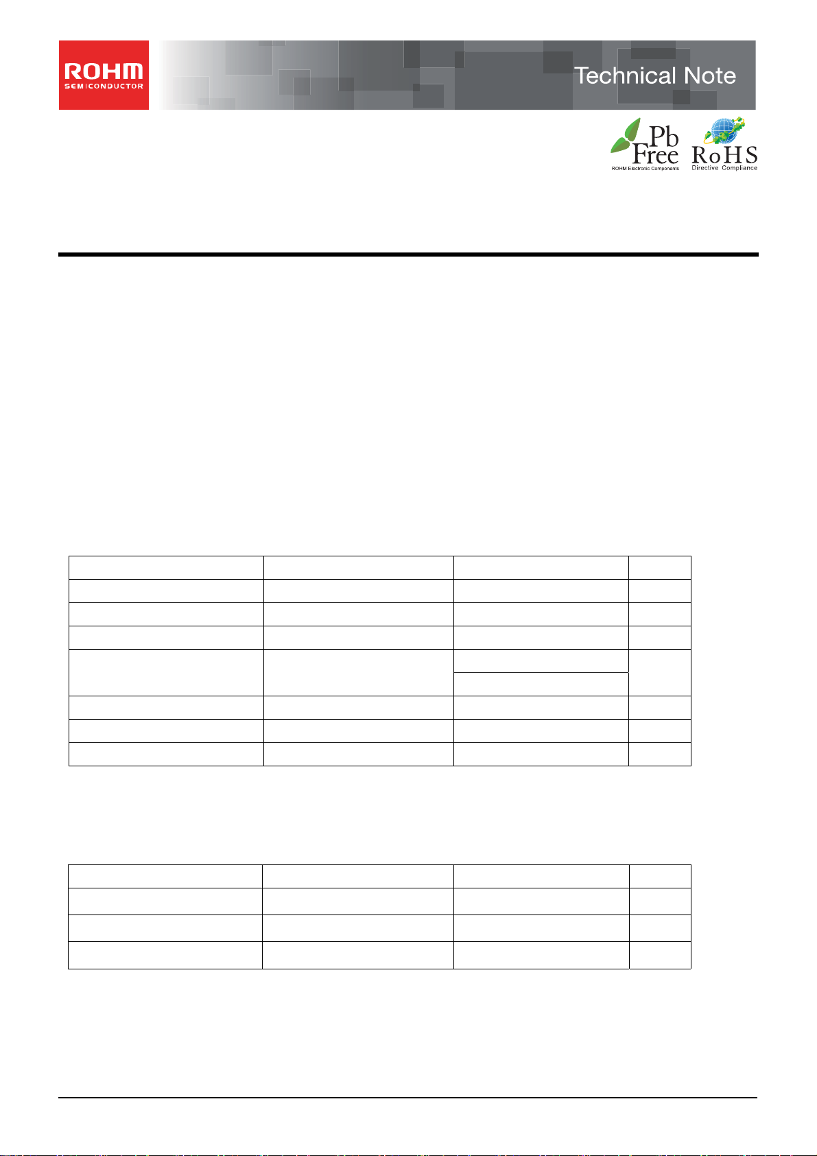
●Thermal Derating Curve
MIN TYP MAX
Limits
Unit Condition
Technical Note
④4.0W
③2.8W
②1.7W
①1.1W
Rating for 70mm×70mm(size), 1.6mm(thickness), copper foil occupation ratio less than 3%,
and use of glass-epoxy substrate.
Fig.1 Power dissipation
www.rohm.com
© 2010 ROHM Co., Ltd. All rights reserved.
2/11
2010.02 - Rev.A
Page 3
BD8229EFV
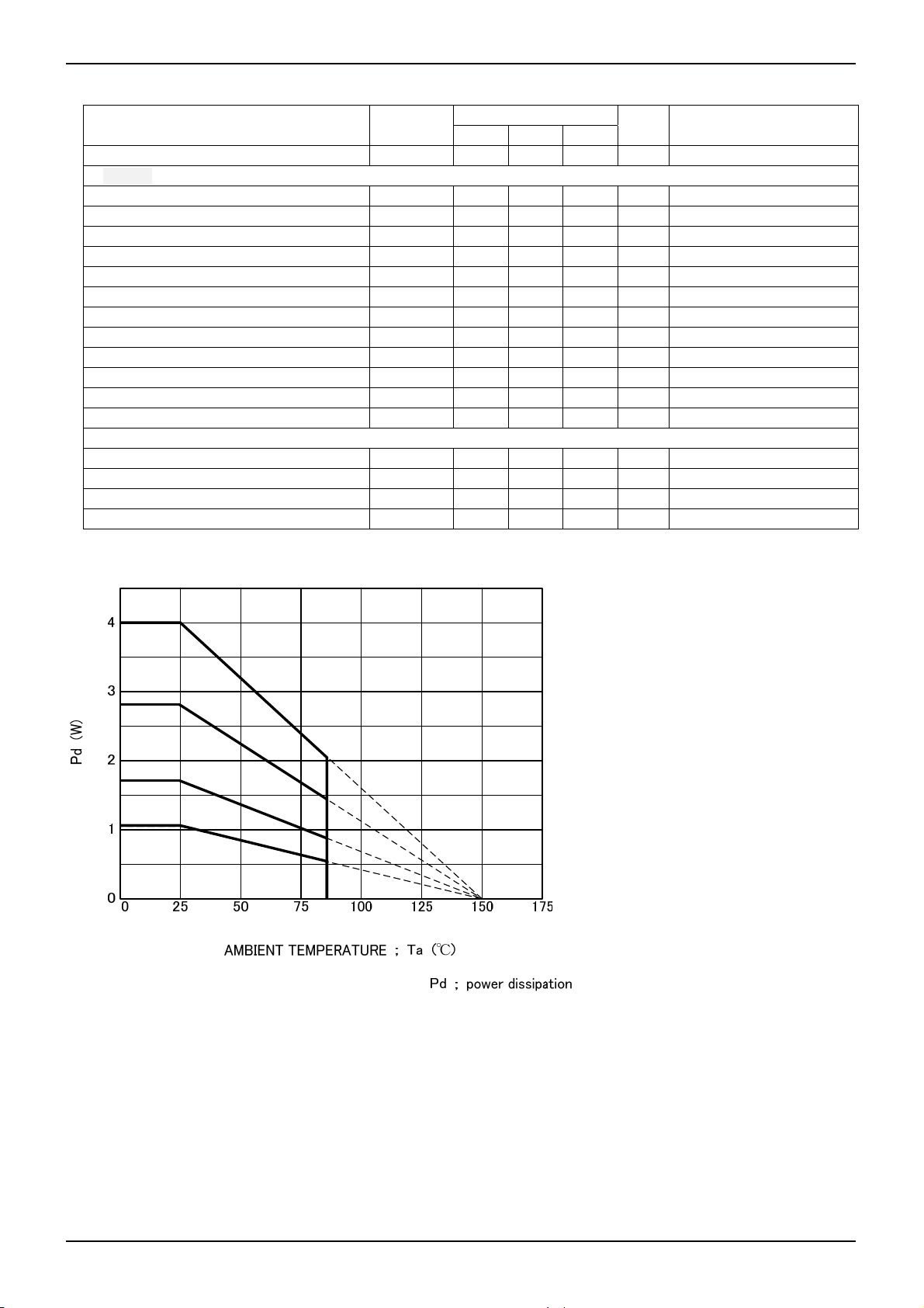
●Package Outlines
Technical Note
D8229EFV
Lot.No
HTSSOP-B24(Unit:mm)
Fig.2 Package Outlines
www.rohm.com
© 2010 ROHM Co., Ltd. All rights reserved.
3/11
2010.02 - Rev.A
Page 4
BD8229EFV
Technical Note
●Block Diagram
24 23 22 21 20 19 18 17 16
IN1
20kΩ
CNT
100kΩ
CNT
20kΩ 20kΩ 47kΩ 47kΩ
IN2-1
1.65V
100kΩ 100kΩ
IN2-2
BIAS
BIAS
47kΩ 47kΩ
IN3
IN4
MUTE
GND
MUTE
15 14 13
PreGND
RSTDET
Pre GND
1.25V
LEVEL
SHIFT
LEVEL
SHIFT
T.S.D
LEVEL
SHIFT
LEVEL
SHIFT
PowVcc11PowGND1
2 3 4 5 6 7 8 9 10 11 12
CH1 CH4
CH2 CH3
PowGND2
PowVcc2
PowVcc1
PowGND1
VO1(-)
VO1(+)
VO2(-)
VO2(+)
VO3(-)
VO3(+)
VO4(-)
VO4(+)
T. S. D:Thermal Shut-Down
Fig.3:Block Diagram
○Pin Descriptions
No. Symbol Description No. Symbol Description
1 PowVcc1 CH1,2 power supply terminal 13 PreVcc Pre,RESET power supply terminal
2 PowGND1 power GND1 14 RSTOUT Reset output
3 VO1(-) Driver CH1 negative output 15 RSTDET Reset detection comparator input
4 VO1(+) Driver CH1 positive output 16 PreGND Pre, Reset Block GND
5 VO2(-) Driver CH2 negative output 17 MUTE MUTE terminal
6 VO2(+) Driver CH2 positive output 18 IN4 CH4 input
7 VO3(-) Driver CH3 negative output 19 IN3 CH3 input
8 VO3(+) Driver CH3 positive output 20 BIAS BIAS input terminal
9 VO4(-) Driver CH4 negative output 21 IN2-2 CH2-2 input
10 VO4(+) Driver CH4 positive output 22 IN2-1 CH2-1 input
11 PowGND2 power GND2 23 CNT Control input terminal
12 PowVcc2 CH3,4 power supply terminal 24 IN1 IN1 input
RSTOUT
PreVcc
PowGND2
PreVcc
PowVcc2
www.rohm.com
© 2010 ROHM Co., Ltd. All rights reserved.
4/11
2010.02 - Rev.A
Page 5

BD8229EFV
Technical Note
●Functional Description
1.The driver can put the mute by switching the terminal MUTE and the terminal CNT to High level and Low level.
The table below shows the logic.
INPUT OUTPUT
MUTE CNT CH1,3,4 CH2
H H ACTIVE LD ON
H L ACTIVE SL ON
L H MUTE LD ON
L L MUTE MUTE
SL : SLED LD : Loading
2.The mute works when the bias terminal (20PIN) becomes 0.7V(typ.) or less. Please set it to 1.3V or more in the state of
use normally.(However, the mute doesn't work as for CH2 at CNT='H'. )
3.When the power-supply voltage becomes 3.8V(typ.) or less, the output terminal becomes the state of the mute.
When the power-supply voltage rises up to 4.0V again, the driver part circuit stands up
4.The threshold voltage of PowVcc2 reset can be calculated by the following expressions.
Vin
R1
RSTDET
PowVcc2
RVCC
10k
RSTOUT
Ω
+
VDET
V
R2
1.25V /1.225V
R2+R1
=Vin
R2
VDET×
・The threshold voltage of PowVcc2 reset can be changed by external resistance R1 and R2.
R1 and R2 recommend the resistance of 100kΩ or less respectively.
・Please make below the voltage of PowVcc2(PIN12) the voltage of the RSTOUT output terminal that is the pull-up (RVCC).
・The characteristic chart of RSTDET and RSTOUT is shown as follows.
RVCC
Hysterisis 25 mV( typ.
RSTOUT(V)
RSTDET(V
)
1.2 5V(typ.
)
)
www.rohm.com
© 2010 ROHM Co., Ltd. All rights reserved.
5/11
2010.02 - Rev.A
Page 6

BD8229EFV
●Example of Recommended Circuit
SP IN
SL/LD SL IN LD IN
BIAS
ACT IN ACT IN
MUTE
RSTDET
Technical Note
RESET出力
PreVcc
24 23 22 21 20 19 18 17 16
Ω
100kΩ100k
LEVEL
SHIFT
CH
1. 65 V
20 k
Ω
BIAS
Ω
47k
47k
47k
Ω
Ω
47 k
Ω
MUTE
Ω
T.S.D
LEVEL
SHIFT
1
CH
2
LEVEL
SHIFT
CH
3
20k
100k
PowVcc11PowGND1
20 k
Ω
CNT
Ω
Pre GND
15 14 13
LEVEL
SHIFT
CH4
Pr e GND
PowGND2
PreVcc
1.25V
PowVcc2
PowVcc2
2 3 4 5 6 7 8 9 10 11 12
M M
PowVcc
Fig.4:Application circuit
PowVcc
www.rohm.com
© 2010 ROHM Co., Ltd. All rights reserved.
6/11
2010.02 - Rev.A
Page 7

BD8229EFV
●The Picture of Application Board Wire Connection(Reference for BD8229EFV)
Technical Note
Fig.5. application board wire connection
www.rohm.com
© 2010 ROHM Co., Ltd. All rights reserved.
7/11
2010.02 - Rev.A
Page 8

BD8229EFV
●The Picture of Application Board Pattern(Reference for BD8229EFV)
BD8229EFV
Technical Note
Top Silkscreen Overlay
Top Layer
Bottom Layer Bottom Silkscreen Overlay
www.rohm.com
© 2010 ROHM Co., Ltd. All rights reserved.
8/11
2010.02 - Rev.A
Page 9

BD8229EFV
●Terminal Equivalent Circuit
50k
50k
20k
47k
Technical Note
47k
×2
positive output
negative output
10k
10k
100k
100k
10k
20k
47k
20k
20k
20k
100k
100k
positive output
10k
negative output
※Resistance in the above-mentioned terminal equivalent circuit chart is 25℃, and a value at typical.
100k
100k
10k
25
20k
20k
5k
www.rohm.com
© 2010 ROHM Co., Ltd. All rights reserved.
9/11
2010.02 - Rev.A
Page 10

BD8229EFV
Technical Note
●Notes for use
1.Absolute maximum ratings
We are careful enough for quality control about this IC. So, there is no problem under normal operation, excluding that it exceeds the
absolute maximum ratings. However, this IC might be destroyed when the absolute maximum ratings, such as impressed voltages or the
operating temperature range, is exceeded, and whether the destruction is short circuit mode or open circuit mode cannot be specified.
Please take into consideration the physical countermeasures for safety, such as fusing, if a particular mode that exceeds the absolute
maximum rating is assumed.
2.Reverse polarity connection
Connecting the power line to the IC in reverse polarity (from that recommended) will damage the part. Please utilize the direction
protection device as a diode in the supply line and motor coil line.
3.Power supply line
Due to return of regenerative current by reverse electromotive force, using electrolytic and ceramic suppress filter capacitors (0.1μF) close
to the IC power input terminals (Vcc and GND) iare recommended. Please note the electrolytic capacitor value decreases at lower
temperatures and examine to dispense physical measures for safety. And, for ICs with more than one power supply, it is possible that rush
current may flow instantaneously due to the internal powering sequence and delays. Therefore, give special consideration to power
coupling capacitance, power wiring, width of GND wiring, and routing of wiring.
4.GND line
Please keep the GND line the lowest potential always, and check the GND voltage when transient voltages are connected to the IC.
5.Thermal design
Do not exceed the power dissipation (Pd) of the package specification rating under actual operation, and please design enough
temperature margins. This product has exposed the frame to the back side of the package, but please note that it is assumed to use heat
radiation efficiency by the heat radiation for this part. Please take the heat radiation pattern on not only the surface of the substrate but
also the back of the substrate widely.
6.Short circuit mode between terminals and wrong mounting
Do not mount the IC in the wrong direction and displacement, and be careful about the reverse-connection of the power connector.
Moreover, this IC might be destroyed when the dust short the terminals between them or GND.
7.Radiation
Strong electromagnetic radiation can cause operation failures.
8.ASO (Area of Safety Operation)
Do not exceed the maximum ASO and the absolute maximum ratings of the output driver.
9.TSD (Thermal Shut-Down)
The TSD is activated when the junction temperature (Tj) exceeds Tjmax, and the output terminal is switched to OPEN. The guarantee and
protection of set are not purpose. Therefore, please do not use this IC after TSD circuit operates, nor use it for assumption that operates
the TSD circuit.
10.Capacitor between output driver and GND
If a large capacitor is connected between the output driver and GND, this IC might be destroyed when Vcc becomes 0V or GND, because
the electric charge accumulated in the capacitor flows to the output driver. Please set said capacitor to smaller than 0.1μF.
11.Inspection by the set circuit board
The stress might hang to IC by connecting the capacitor to the terminal with low impedance. Then, please discharge electricity in each and
all process. Moreover, when attaching or detaching from jig in the inspection process, please turn off the power before mounting the IC,
and turn on after mounting the IC, and vice versa. In addition, please take into consideration the countermeasures for electrostatic
damage, such as giving the earth in assembly process, transportation or preservation.
12.Input terminal
This IC is a monolithic IC, and has P
+
isolation and P substrate for the element separation. Therefore, a parasitic PN junction is firmed in
this P-layer and N-layer of each element. For instance, the resistor or the transistor is connected to the terminal as shown in the figure
below. When the GND voltage potential is greater than the voltage potential at Terminals A on the resistor, at Terminal B on the transistor,
the PN junction operates as a parasitic diode. In addition, the parasitic NPN transistor is formed in said parasitic diode and the N layer of
surrounding elements close to said parasitic diode. These parasitic elements are formed in the IC because of the voltage relation. The
parasitic element operating causes the interference of circuit operation, then the wrong operation and destruction. Therefore, please be
careful so as not to operate the parasitic elements by impressing to input terminals lower voltage than GND (P substrate). Please do not
apply the voltage to the input terminal when the power-supply voltage is not impressed. Moreover, please impress each input terminal
lower than the power-supply voltage or equal to the specified range in the guaranteed voltage when the power-supply voltage is
impressing.
Terminal-A
P
Parasitic
element
+
Resistor
Terminal-A
+
P
P
P-Substrate
GND
Parasitic
element
Terminal-B
P
Parasitic
element
CB
+
Transistor(NPN)
E
+
P
P
P-Substrate
GND
GND
Terminal-B
Surrounding
elements
C
B
E
Parasitic
element
GND
Simplified structure of IC
13Earth wiring pattern
If small signal GND and large current GND exist, disperse their pattern. In addition, for voltage change by pattern wiring impedance and
large current not to change voltage of small signal GND, each ground terminal of IC must be connected at the one point on the set circuit
board. As for GND of external parts, it is similar to the above-mentioned.
14Please make below the voltage of PowVcc2(PIN12) the voltage of the RSTOUT output terminal that is the pull-up (RVCC).
www.rohm.com
© 2010 ROHM Co., Ltd. All rights reserved.
10/11
2010.02 - Rev.A
Page 11

BD8229EFV
●Ordering part number
B D 8 2 2 9 E F V - E 2
Technical Note
Part No. Part No.
SSOP-B24
7.8 ± 0.2
(MAX 8.15 include BURR)
24
7.6 ± 0.3
5.6 ± 0.2
1
1.15 ± 0.1
0.1
0.65
0.22 ± 0.1
Package
EFV: HTSSOP-B24
Packaging and forming specification
E2: Embossed tape and reel
<Tape and Reel information>
Embossed carrier tapeTape
13
0.3Min.
12
0.15 ± 0.1
0.1
(Unit : mm)
Quantity
Direction
of feed
2000pcs
E2
The direction is the 1pin of product is at the upper left when you hold
()
reel on the left hand and you pull out the tape on the right hand
Direction of feed
Reel
1pin
Order quantity needs to be multiple of the minimum quantity.
∗
www.rohm.com
© 2010 ROHM Co., Ltd. All rights reserved.
11/11
2010.02 - Rev.A
Page 12

Notes
No copying or reproduction of this document, in part or in whole, is permitted without the
consent of ROHM Co.,Ltd.
The content specied herein is subject to change for improvement without notice.
The content specied herein is for the purpose of introducing ROHM's products (hereinafter
"Products"). If you wish to use any such Product, please be sure to refer to the specications,
which can be obtained from ROHM upon request.
Examples of application circuits, circuit constants and any other information contained herein
illustrate the standard usage and operations of the Products. The peripheral conditions must
be taken into account when designing circuits for mass production.
Great care was taken in ensuring the accuracy of the information specied in this document.
However, should you incur any damage arising from any inaccuracy or misprint of such
information, ROHM shall bear no responsibility for such damage.
The technical information specied herein is intended only to show the typical functions of and
examples of application circuits for the Products. ROHM does not grant you, explicitly or
implicitly, any license to use or exercise intellectual property or other rights held by ROHM and
other parties. ROHM shall bear no responsibility whatsoever for any dispute arising from the
use of such technical information.
Notice
The Products specied in this document are intended to be used with general-use electronic
equipment or devices (such as audio visual equipment, ofce-automation equipment, communication devices, electronic appliances and amusement devices).
The Products specied in this document are not designed to be radiation tolerant.
While ROHM always makes ef forts to enhance the quality and reliability of its Products, a
Product may fail or malfunction for a variety of reasons.
Please be sure to implement in your equipment using the Products safety measures to guard
against the possibility of physical injury, re or any other damage caused in the event of the
failure of any Product, such as derating, redundancy, re control and fail-safe designs. ROHM
shall bear no responsibility whatsoever for your use of any Product outside of the prescribed
scope or not in accordance with the instruction manual.
The Products are not designed or manufactured to be used with any equipment, device or
system which requires an extremely high level of reliability the failure or malfunction of which
may result in a direct threat to human life or create a risk of human injury (such as a medical
instrument, transportation equipment, aerospace machinery, nuclear-reactor controller, fuelcontroller or other safety device). ROHM shall bear no responsibility in any way for use of any
of the Products for the above special purposes. If a Product is intended to be used for any
such special purpose, please contact a ROHM sales representative before purchasing.
If you intend to export or ship overseas any Product or technology specied herein that may
be controlled under the Foreign Exchange and the Foreign Trade Law, you will be required to
obtain a license or permit under the Law.
Thank you for your accessing to ROHM product informations.
More detail product informations and catalogs are available, please contact us.
ROHM Customer Support System
www.rohm.com
© 2010 ROHM Co., Ltd. All rights reserved.
http://www.rohm.com/contact/
R1010
A
 Loading...