

LED Drivers for LCD Backlights
Backlight LED Driver
for Small LCD Panels (Charge Pump Type)
BD82103GWL
●Description
BD82103GWL is charge pump type 2 light or 3 light parallel LED driver for the portable instruments.
This IC not only ensures efficient boost by automatically changing the boost rate but also works as a constant current driver
in 16 steps, so that the driving current can be adjusted finely. This IC is best suited to turn on white LEDs that require
high-accuracy LED brightness control.
●Features
1) 2light or 3light parallel LED driver is mounted
2) 16-step LED current adjust function
3) Inter-LED relative current accuracy: 5% or less
4) Driving control via a single-line digital control interface
5) Automatic transition charge pump type DC/DC converter (×1,×1.5, x2)
6) High efficiency achieved (Maximum over 93%)
7) It transits for the most suitable power operating by the LED terminal process
of the 3rd light when 2 light driving
8) Various protection functions such as output voltage protection and thermal shutdown circuit are mounted.
9) Package : UCSP50L1 (Thick 0.55mm MAX, Pin pitch 0.4mm) CSP11pin package
●Absolute Maximum Ratings (Ta=25℃)
Parameter Symbol Ratings Unit
Power supply voltage VMAX 7 V
No.11040EBT34
Input voltage ( EN ) Vdin GND-0.3 ~ VBAT+0.3 V
Power dissipation Pd 730 mW
Operating temperature range Topr -30 ~ +85 ℃
Storage temperature range Tstg -55 ~ +150 ℃
Note 1) The measurement value which was mounted on the PCB by ROHM.
When a glass epoxy substrate (70mm × 70mm × 1.6mm) has been mounted, this loss will decrease
5.84mW/℃ if Ta is higher than or equal to 25℃.
●Operating Conditions (Ta = -30 ~ 85
Parameter Symbol
Operating power supply voltage VBAT 2.7 ~ 5.5 V
*This chip is not designed to protect itself against radioactive rays.
*This material may be changed on its way to designing.
*This material is not the official specification.
℃)
Ratings
Unit
www.rohm.com
1/9
© 2011 ROHM Co., Ltd. All rights reserved.
2011.06 - Rev.B

BD82103GWL
●Electrical Characteristics (Unless otherwise noted, Ta = +25℃, VBAT=3.6V)
Parameter Symbol
Current Consumption
Quiescent Current Iq - 0.1 1 μA EN=0V
Current Consumption1 Idd1 - 1.0 2.4 mA x1.0 Mode, Except LED current
Current Consumption2 Idd2 - 2.0 3.5 mA x2.0 Mode, Except LED current
Charge Pump
Oscillator frequency fOSC 0.56 0.85 1.14 MHz
Current Source
LED maximum current ILED-max 18 20 22 mA VBAT≥3.0V
Min. Typ. Max.
Limits
Unit Condition
Technical Note
LED current accuracy ILED-diff - - 10.0 %
LED current matching ILED-match - 0.5 5.0 %
LED control voltage VLED - 0.15 0.25 V
Logic control terminal
Low threshold voltage VIL - - 0.4 V EN
High threshold voltage VIH 1.4 - - V EN
High level Input current IIH - 0 1 μA EN=Vin
Low level Input current IIL -1 0 - μA EN=0V
Minimum EN High time THI 0.05 - 100 μsec Described in Fig.5
Minimum EN Low time TLO 0.3 - 100 μsec Described in Fig.5
EN Off Timeout TOFF 1 - - msec Described in Fig.5
Latch time TLAT 1 - - msec Described in Fig.5
Access available time Tacc 1 - - msec Described in Fig.5
When LED current 10.0mA
setting and LED terminal voltage 1.0V
When LED current 10.0mA
setting and LED terminal voltage 1.0V
minimum voltage
at LED1~LED3 pins
www.rohm.com
2/9
© 2011 ROHM Co., Ltd. All rights reserved.
2011.06 - Rev.B
BD82103GWL
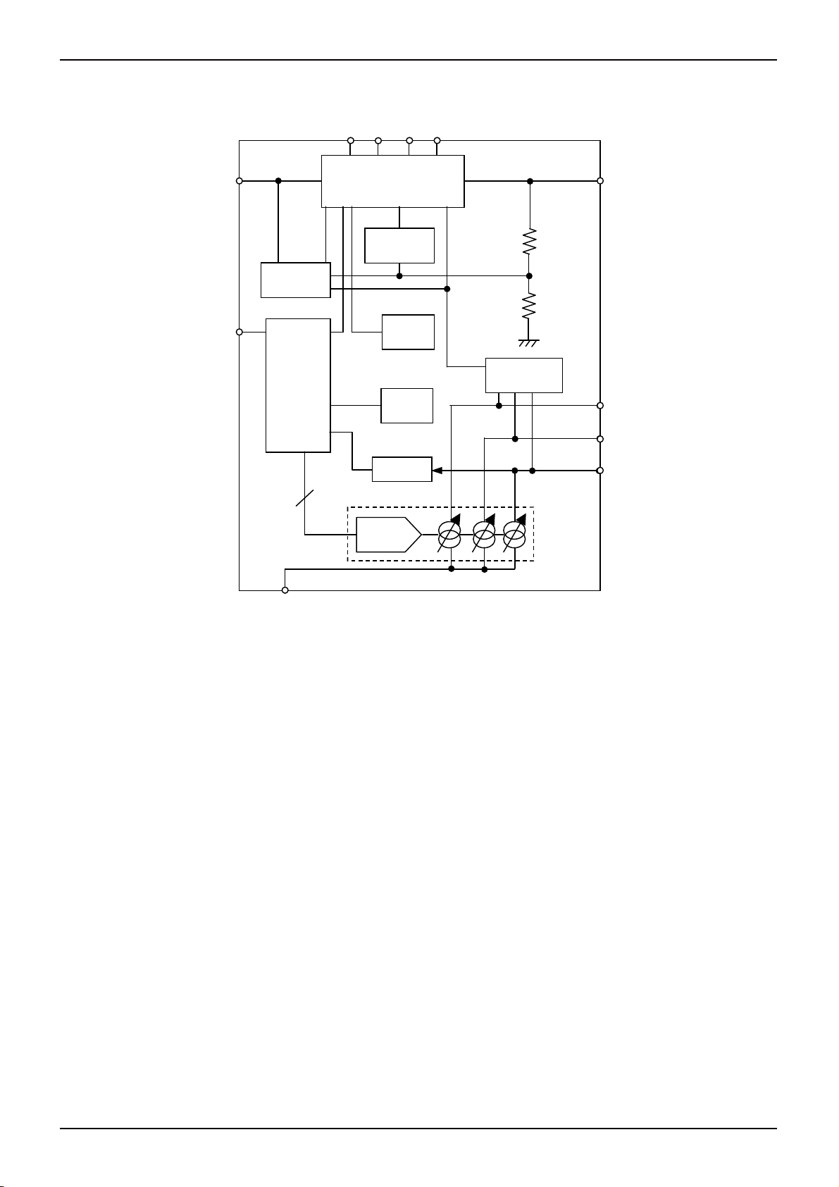
●Block Diagram
VBAT
EN
Charge Pump
Mode Control
Enable/
Brightness
Control
4
GND
C1N
C1P
C2P
C2N
×1, ×1.5, ×2
Charge pump
Over Voltage
Protect
OSC
TSD
LED3 DET
Current
DAC
Pin number 11pin
Fig. 1 Block Diagram
Technical Note
VOUT
Vout Cont rol
LED1
LED2
LED3
www.rohm.com
3/9
© 2011 ROHM Co., Ltd. All rights reserved.
2011.06 - Rev.B
BD82103GWL
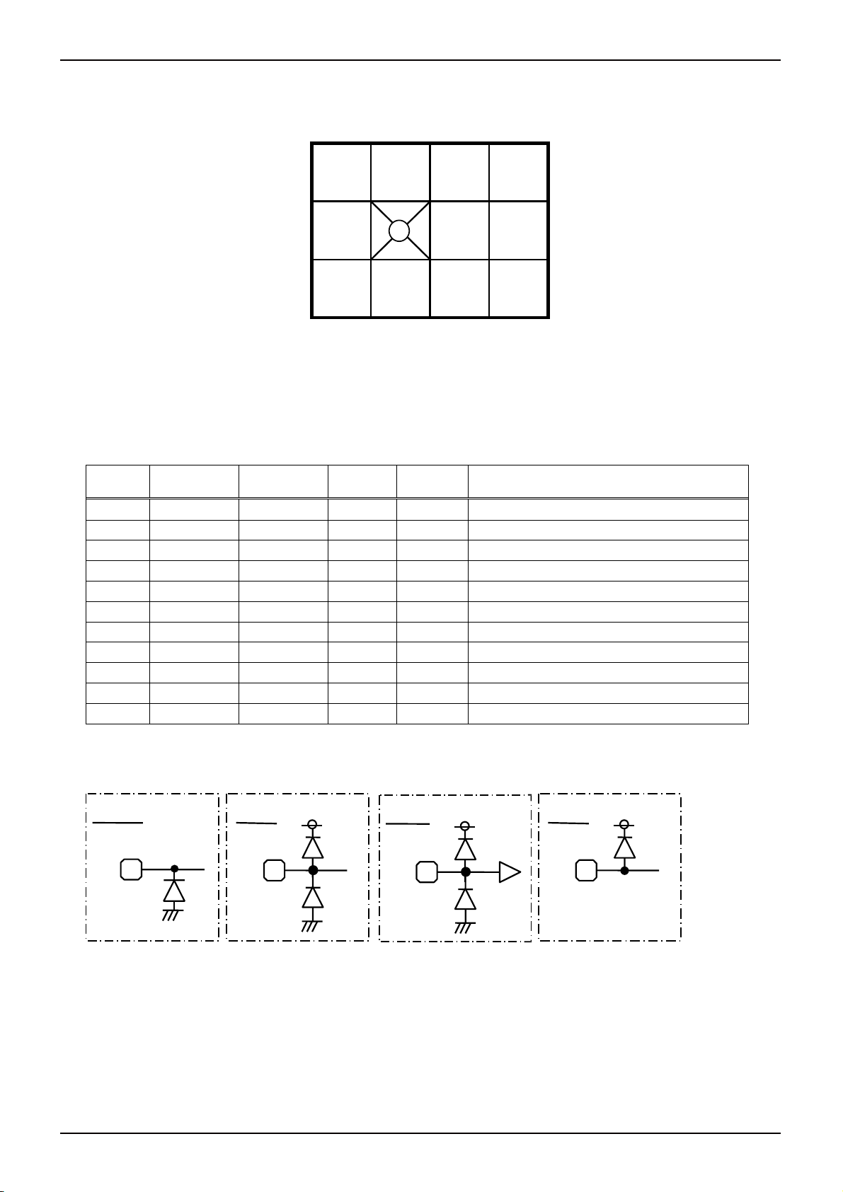
●Pin Configuration [Bottom View]
●Pin Descriptions
Pin No. Terminal No. Pin name In/Out Type Function
LED1 GND VBAT C1N
C
index
LED2
B
LED3 VOUT C2N C2P
A
1234
Fig. 2 Pin Configuration
EN C1P
Technical Note
1 C3 VBAT - A Power supply
2 B4 C1P In/Out A Flying capacitor pin positive (+) side
3 C4 C1N
4 A4 C2P
5 A3 C2N
6 A2 VOUT Out A Charge pump output
7 B3 EN In C ON/OFF and dimming control
8 C1 LED1 Out
9 B1 LED2 Out
10 A1 LED3 Out
11 C2 GND - D GND
●Pin ESD Type
Type A
PAD
GND
Type B
PAD
GND
In/Out
In/Out
In/Out
Type C
VBAT
PAD
Fig. 4 Pin ESD Type
B Flying capacitor pin negative (-) side
A Flying capacitor pin positive (+) side
B Flying capacitor pin negative (-) side
A
A
A
GND
LED current driver output 1
LED current driver output 2
LED current driver output 3
VBAT
Type D
PAD
VBAT
www.rohm.com
4/9
© 2011 ROHM Co., Ltd. All rights reserved.
2011.06 - Rev.B
BD82103GWL
●Separate Function Description
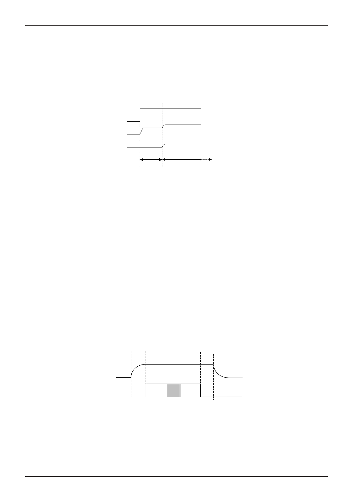
(1) LED driver
・Register access control protocol
LED current is controlled by only EN terminal. It is possible to access the register inside of this chip by using the
protocol below. LED driver ON/OFF, selecting the mode is operated by accessing the registers with using this protocol.
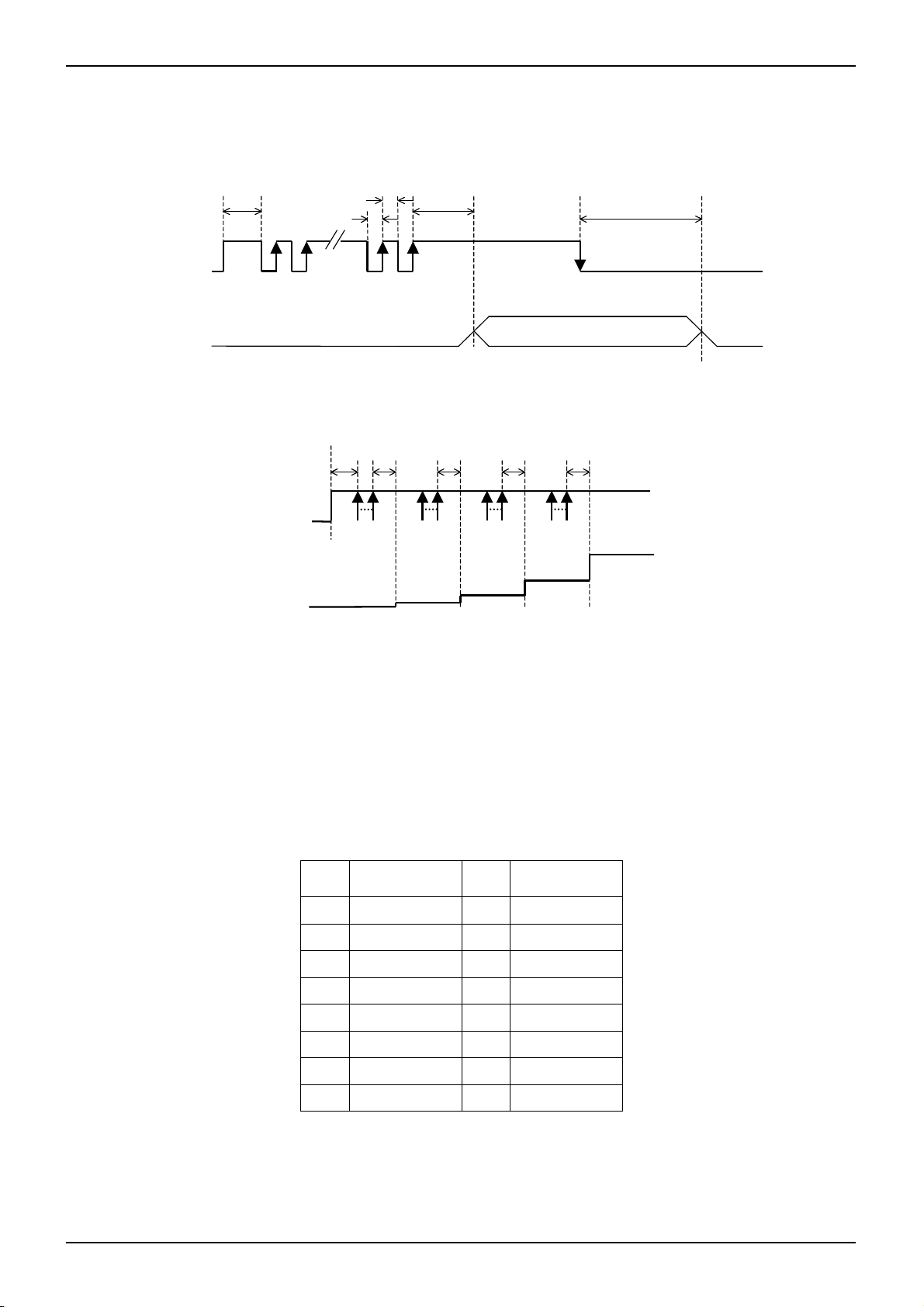
T
acc
Technical Note
T
T
LO
T
HI
LAT
T
OFF
( Note )
・In the case of N > 16, BD82103GWL selects the mode of N = 16.
・LED current is changed by the pulse of EN pin.
Be careful to noise of EN signal.
・Reset BD82103GWL when the set is unusual. (Keep EN=L over Toff time.)
・LED current level
The interface records rising edges of the EN pin and decodes them into 16 different indicated in following table.
EN
12
LED Current Setting
EN
LED Current
n
(N≦16)
n-1
Fig.5 Register access protocol
T
T
T
LAT
acc
16pulse 15pulse 14pulse
OFF
LAT
0.125mA
0.25mA
T
LAT
13pulse
0.5mA
T
LAT
Fig.6 Slope control example
Data
Output current
[mA]
Data
Output current
[mA]
1 20.0 9 5.0
n 0 0
1mA
2 17.0 10 4.0
3 14.0 11 3.0
4 12.0 12 2.0
5 10.0 13 1.0
6 8.5 14 0.5
7 7.0 15 0.25
8 6.0 16 0.125
www.rohm.com
5/9
© 2011 ROHM Co., Ltd. All rights reserved.
2011.06 - Rev.B
BD82103GWL
V
(2) Charge pump
a) Description of operations
Pin voltage comparison takes place at Vout control section, and then Vout generation takes place so that the LED
cathode voltage with the highest Vf is set to 0.2V. A boost rate is changed automatically to a proper one at the Charge
Pump Mode Control section so that operation can take place at possible low boost rate. In addition, if the output
voltage falls below 1.5V, this IC is reset for short-circuit at output.
b) Soft start function
BD82103GWL have a soft start function that prevents the rush current.
EN/LED*
VOUT
Technical Note
T
OFF
I
LED
Soft Start Ordinal mode
Fig.7 Soft Start
c) Automatic boost rate change
The boost rate automatically switches to the best mode.
* (×1 mode ×1.5 mode) or (×1.5 mode ×2 mode)
If a battery voltage drop occurs BD82103GWL cannot maintain the LED constant current, and then mode transition
begins.
* (×1.5 mode ×1 mode) or (×2 mode ×1.5 mode)
If a battery voltage rise occurs, VOUT and VBAT detection are activated, and then mode transition begins.
(3) UVLO (Under Voltage Lock Out)
If the input voltage falls below 2.2V, BD82103GWL is shut down to prevent malfunction due to ultra-low voltage.
(4) OVP (Over Voltage Protection)
This circuit protects this IC against damage when the C/P output voltage (VOUT) rises extremely for some external
factors.
(5) Thermal shutdown (TSD)
To protect this IC against thermal damage or heat-driven uncontrolled operations, this circuit turns off the output if the
chip temperature rises over 175℃. In addition, it turns on the output if the temperature returns to the normal
temperature. Because the built-in thermal protection circuit is intended to protect the IC itself, the thermal shutdown
detection temperature must be set to below 175℃ in thermal design.
(6 ) Power sequence
EN signal must be released after VBAT voltage enough rise up.
Prohibit the VBAT rise up during EN=”H”.
BAT
EN
Fig.8 Power sequence
www.rohm.com
6/9
© 2011 ROHM Co., Ltd. All rights reserved.
2011.06 - Rev.B

BD82103GWL
●Application Circuit Example (3 light)
Battery
VBAT
Cin
=1μF
EN
Pulse
Generator
Charge Pump
Mode Control
●Application Circuit Example (2 light)
Battery
VBAT
Cin
=1μF
EN
Pulse
Generator
Charge Pump
Mode Control
Enable/
Brightness
Control
4
GND
Enable/
Brightness
Control
4
GND
C1P
C2
C2N
C2P
C1
C1N
×1, ×1.5, ×2
Charge pump
Over Voltage
Protect
OSC
Vout Control
TSD
LED3 DET
Current
DAC
Fig.9 Application Circuit Example 1
C1P
C2
C2N
C2P
C1
C1N
×1, ×1.5, ×2
Charge pump
Over Voltage
Protect
OSC
Vout Control
TSD
LED3 DET
Current
DAC
Fig.10 Application Circuit Example 2
VOUT
LED1
LED2
LED3
VOUT
LED1
LED2
LED3
Cout
=1μF
Cout
=1μF
Technical Note
www.rohm.com
7/9
© 2011 ROHM Co., Ltd. All rights reserved.
2011.06 - Rev.B

BD82103GWL
●Notes for use
(1) Absolute Maximum Ratings
An excess in the absolute maximum ratings, such as supply voltage, temperature range of operating conditions, etc.,
can break down devices, thus making impossible to identify breaking mode such as a short circuit or an open circuit.
If any special mode exceeding the absolute maximum ratings is assumed, consideration should be given to take
physical safety measures including the use of fuses, etc.
(2) Power supply and ground line
Design PCB pattern to provide low impedance for the wiring between the power supply and the ground lines.
Pay attention to the interference by common impedance of layout pattern when there are plural power supplies and
ground lines. Especially, when there are ground pattern for small signal and ground pattern for large current included
the external circuits, please separate each ground pattern. Furthermore, for all power supply pins to ICs, mount a
capacitor between the power supply and the ground pin. At the same time, in order to use a capacitor, thoroughly
check to be sure the characteristics of the capacitor to be used present no problem including the occurrence of
capacity dropout at a low temperature, thus determining the constant.
(3) Ground voltage
Make setting of the potential of the ground pin so that it will be maintained at the minimum in any operating state.
Furthermore, check to be sure no pins are at a potential lower than the ground voltage including an actual electric
transient.
(4) Short circuit between pins and erroneous mounting
In order to mount ICs on a set PCB, pay thorough attention to the direction and offset of the ICs. Erroneous mounting
can break down the ICs. Furthermore, if a short circuit occurs due to foreign matters entering between pins or between
the pin and the power supply or the ground pin, the ICs can break down.
(5) Operation in strong electromagnetic field
Be noted that using ICs in the strong electromagnetic field can malfunction them.
(6) Input pins
In terms of the construction of IC, parasitic elements are inevitably formed in relation to potential. The operation of the
parasitic element can cause interference with circuit operation, thus resulting in a malfunction and then breakdown of
the input pin. Therefore, pay thorough attention not to handle the input pins, such as to apply to the input pins a voltage
lower than the ground respectively, so that any parasitic element will operate. Furthermore, do not apply a voltage to
the input pins when no power supply voltage is applied to the IC. In addition, even if the power supply voltage is
applied, apply to the input pins a voltage lower than the power supply voltage or within the guaranteed value of
electrical characteristics.
(7) External capacitor
In order to use a ceramic capacitor as the external capacitor, determine the constant with consideration given to a
degradation in the nominal capacitance due to DC bias and changes in the capacitance due to temperature, etc.
(8) Thermal shutdown circuit (TSD)
This IC builds in a thermal shutdown (TSD) circuit. When junction temperatures become detection temperature or
higher, the thermal shutdown circuit operates and turns a switch OFF. The thermal shutdown circuit, which is aimed at
isolating the IC from thermal runaway as much as possible, is not aimed at the protection or guarantee of the IC.
Therefore, do not continuously use the IC with this circuit operating or use the IC assuming its operation.
(9) Thermal design
Perform thermal design in which there are adequate margins by taking into account the permissible dissipation (Pd) in
actual states of use.
(10) LDO
Use each output of LDO by the independence. Don’t use under the condition that each output is short-circuited
because it has the possibility that an operation becomes unstable.
(11) About the pin for the test, the un-use pin
Prevent a problem from being in the pin for the test and the un-use pin under the state of actual use. Please refer to a
function manual and an application notebook. And, as for the pin that doesn't specially have an explanation, ask our
company person in charge.
(12) About the rush current
For ICs with more than one power supply, it is possible that rush current may flow instantaneously due to the internal
powering sequence and delays. Therefore, give special consideration to power coupling capacitance, power wiring,
width of ground wiring, and routing of wiring.
(13) About the function description or application note or more.
The function description and the application noteb
materials aren't always guaranteed. Please design application by having fully examination and evaluation include the
external elements.
Technical Note
ook are the design materials to design a set. So, the contents of the
www.rohm.com
8/9
© 2011 ROHM Co., Ltd. All rights reserved.
2011.06 - Rev.B

BD82103GWL
●Ordering part number
B D 8 2 1 0 3 G W L - E 2
Part No. Part No. Package
UCSP50L1
(BD82103GWL)
1PIN MARK
11-φ0.2±0.05
0.05
BA
(φ0.15)INDEX POST
0.3±0.05
B
A
1.8±0.05
0.08 S
2
<Tape and Reel information>
1.5±0.05
0.1±0.05
0.55MAX
S
A
3C1
4
P=0.4×3
0.35±0.05
B
P=0.4×2
(Unit : mm)
Quantity
Direction
of feed
GWL: UCSP50L1
Embossed carrier tapeTape
3000pcs
E2
The direction is the 1pin of product is at the upper left when you hold
()
reel on the left hand and you pull out the tape on the right hand
Reel
1pin
Order quantity needs to be multiple of the minimum quantity.
∗
Packaging and forming specification
E2: Embossed tape and reel
Technical Note
Direction of feed
www.rohm.com
9/9
© 2011 ROHM Co., Ltd. All rights reserved.
2011.06 - Rev.B

Notes
No copying or reproduction of this document, in part or in whole, is permitted without the
consent of ROHM Co.,Ltd.
The content specied herein is subject to change for improvement without notice.
The content specied herein is for the purpose of introducing ROHM's products (hereinafter
"Products"). If you wish to use any such Product, please be sure to refer to the specications,
which can be obtained from ROHM upon request.
Examples of application circuits, circuit constants and any other information contained herein
illustrate the standard usage and operations of the Products. The peripheral conditions must
be taken into account when designing circuits for mass production.
Great care was taken in ensuring the accuracy of the information specied in this document.
However, should you incur any damage arising from any inaccuracy or misprint of such
information, ROHM shall bear no responsibility for such damage.
The technical information specied herein is intended only to show the typical functions of and
examples of application circuits for the Products. ROHM does not grant you, explicitly or
implicitly, any license to use or exercise intellectual property or other rights held by ROHM and
other parties. ROHM shall bear no responsibility whatsoever for any dispute arising from the
use of such technical information.
The Products specied in this document are intended to be used with general-use electronic
equipment or devices (such as audio visual equipment, of ce-automation equipment, communication devices, electronic appliances and amusement devices).
The Products specied in this document are not designed to be radiation tolerant.
While ROHM always makes efforts to enhance the quality and reliability of its Products, a
Product may fail or malfunction for a variety of reasons.
Please be sure to implement in your equipment using the Products safety measures to guard
against the possibility of physical injury, re or any other damage caused in the event of the
failure of any Product, such as derating, redundancy, re control and fail-safe designs. ROHM
shall bear no responsibility whatsoever for your use of any Product outside of the prescribed
scope or not in accordance with the instruction manual.
The Products are not designed or manufactured to be used with any equipment, device or
system which requires an extremely high level of reliability the failure or malfunction of which
may result in a direct threat to human life or create a risk of human injury (such as a medical
instrument, transportation equipment, aerospace machinery, nuclear-reactor controller, fuelcontroller or other safety device). ROHM shall bear no responsibility in any way for use of any
of the Products for the above special purposes. If a Product is intended to be used for any
such special purpose, please contact a ROHM sales representative before purchasing.
If you intend to export or ship overseas any Product or technology specied herein that may
be controlled under the Foreign Exchange and the Foreign Trade Law, you will be required to
obtain a license or permit under the Law.
Notice
www.rohm.com
© 2011 ROHM Co., Ltd. All rights reserved.
Thank you for your accessing to ROHM product informations.
More detail product informations and catalogs are available, please contact us.
ROHM Customer Support System
http://www.rohm.com/contact/
R1120
A
 Loading...