

A
Power Supply ICs for TFT-LCD Panels
5V Input Multi-channel
System Power Supply ICs
BD8163EFV
●Description
The BD8163EFV is a system power supply IC for TFT panels. A 1-chip IC providing a total of four voltages required for TFT
panels, i.e., logic voltage, sauce voltage, gate high-level, and gate low-level voltage, thus constructing a TFT panel power
supply with minimal components required.
●Features
1) Operates in an operating voltage range as low as 2.1 V to 6. 0 V.
2) Incorporates a step-up DC/DC converter.
3) Incorporates a 2.5 V regulator.
4) Incorporates positive and negative-side charge pumps.
5) Switching frequency of 1100 kHz
6) DC/DC converter feedback voltage of 1.24 V ± 1%
7) Incorporates a gate shading function
8) Under-voltage lockout protection circuit
9) Thermal shutdown circuit
10) Overcurrent protection circuit
11) HTSSOP-B24 package
●Applications
Liquid crystal TV, PC monitor, and TFT-LCD panel
●Absolute maximum ratings (Ta = 25℃)
Parameter Symbol Ratings Unit
No.10035EAT13
Power supply voltage VCC 7 V
Vo1 voltage Vo1 19 V
Vo2 voltage Vo2 32 V
SW voltage Vsw 19 V
Maximum junction temperature Tjmax 150 ℃
Power dissipation Pd 1100* mW
Operating temperature range Topr -40 to 125 ℃
Storage temperature range Tstg -55 to 150 ℃
* Reduced by 4.7 mW/℃ over 25℃, when mounted on a glass epoxy board. (70 mm 70 mm 1.6 mm).
●Recommended Operating Ranges
Ratings
Parameter Symbol
Min. Max.
Power supply voltage VCC 2.1 6 V
Vo1 voltage Vo1 8 18 V
Vo2 voltage Vsw — 18 V
SW Current Isw — 1.8 A
Vo2 Current Vo2 — 30 V
Unit
www.rohm.com
© 2010 ROHM Co., Ltd. All rights reserved.
1/21
2010.12 - Rev.
A
BD8163EFV
●Electrical Characteristics (Unless otherwise specified, VCC = 5 V; Vo1 = 15 V; Vo2 = 25 V; Ta = 25℃)
1 DC/DC Converter Block
Limits
Parameter Symbol
Unit Conditions
Min. Typ. Max.
[Soft start]
Source current Iso 6 10 14 μA Vss = 0.5 V
Sinking current Isi 0.1 0.2 1.0 mA Vss = 0.5 V, VDD = 1.65 V
[Error amp]
Technical Note
Input bias current 1 I
Feedback voltage 1 V
— 0.1 0.5 μA
FB1
1.227 1.240 1.253 V Buffer
FB1
Voltage gain AV — 200 — V/V *
Sinking current IoI 25 50 100 μA VFB = 1.5 V VCOMP = 0.5 V
Source current Ioo -100 -50 -25 μA VFB = 1.0 V VCOMP = 0.5 V
[SW]
ON resistance N-channel R
Leak current N-channel I
Maximum duty cycle D
50 200 600 mΩ *
ON_N
— — 10 μA Vsw = 18 V
LEAKN
75 85 95 %
MAX
[Overcurrent protection]
Saw current limit Insw 2 3 — A *
2. Regulator controller
Limits
Parameter Symbol
Unit Conditions
Min. Typ. Max.
[Error amp]
VDD voltage VDD 2.4 2.5 2.6 V
Maximum base current I
Line regulation RegI — 10 30 mV Vcc = 4.5 V to 5.5 V
Load regulation RegL — 10 50 mV Io = 10 mA to 100 mA
[Under-voltage lockout protection]
Off threshold voltage V
On threshold voltage V
This product is not designed for protection against radioactive rays.
* Design guarantee (No total shipment inspection is made.)
www.rohm.com
© 2010 ROHM Co., Ltd. All rights reserved.
2 7 15 mA
BMAX
1.7 1.8 1.9 V
ROFF
1.6 1.7 1.8 V
RON
2/21
2010.12 - Rev.
A
BD8163EFV
3. Charge pump
Parameter Symbol
[Error amp]
Technical Note
Limits
Unit Conditions
Min. Typ. Max.
Input bias current 2 I
Input bias current 3 I
Feedback voltage 2 V
Feedback voltage 3 V
— 0.1 0.5 μA
FB2
— 0.1 0.5 μA
FB3
1.183 1.240 1.307 V
FB2
0.15 0.2 0.25 V
FB3
[Delay start block]
Source current I
Sinking current I
3 5 7 μA VDLS = 0.5V
DSO
0.1 0.5 1.0 mA VDLS = 0.5V
DSI
Startup voltage VST 0.45 0.60 0.75 V
[Switch]
ON resistance N-channel R
ON resistance P-channel R
0.5 2 4 Ω Io = 10 mA *
ON_NC
0.5 4 8 Ω Io = -10 mA *
ON_PC
[Diode]
Voltage of diode Vf
600 710 800
mV Io = 10 mA
[Gate shading block]
ON resistance N-channel R
ON resistance P-channel R
Leak current N-channel I
Leak current P-channel I
LEAK_NG
LEAK_PG
2 10 20 Ω Io = 10 mA *
ON_NGS
2 10 20 Ω Io = -10 mA *
ON_PGS
S — — 10 μA
S — — 10 μA
High voltage IGH VDD × 0.7 VDD — V
Low voltage IGL — 0 VDD × 0.3 V
Input current IIG 8 16.5 30 μA IG = 3.3 V
This product is not designed for protection against radioactive rays.
* Design guarantee (No total shipment inspection is made.)
www.rohm.com
© 2010 ROHM Co., Ltd. All rights reserved.
3/21
2010.12 - Rev.

A
BD8163EFV
4. Overall
Parameter Symbol
[Reference block]
Technical Note
Limits
Unit Conditions
Min. Typ. Max.
Reference voltage V
Drive current I
1.215 1.240 1.265 V
REF
— 23 — mA VREF = 0 V
REF
Load regulation ∆V — 1 10 mV IREF = -1 mA
[Oscillator]
Oscillating frequency Fosc 0.94 1.1 1.265 MHz
[Oscillator]
DET 1 On threshold voltage V
DET 1 Off threshold voltage V
DET 2 On threshold voltage V
DET 2 Off threshold voltage V
DET 3 On threshold voltage V
1.7 1.8 1.9 V
DON1
1.6 1.7 1.8 V
DOFF1
1.02 1.12 1.22 V
DON2
0.90 1.00 1.10 V
DOFF2
0.25 0.30 0.35 V
DON3
DET 3 Off threshold voltage V
DET 4 On threshold voltage V
DET 4 Off threshold voltage V
0.35 0.41 0.47 V
DOFF3
1.02 1.12 1.22 V
DON4
0.90 1.00 1.10 V
DOFF4
[Device]
Average circuit current Icc 0.5 2 5 mA No switching
This product is not designed for protection against radioactive rays.
www.rohm.com
© 2010 ROHM Co., Ltd. All rights reserved.
4/21
2010.12 - Rev.

A
BD8163EFV
●Reference Data (Unless otherwise specified, Ta = 25℃)
1
0.8
0.6
0.4
0.2
SUPPLY CURRENT : ICC[mA] .
0
01.5 34.56
Fig. 1 Total Supply Current 1
125℃
25℃
-40℃
SUPPLY VOLTAGE : VCC [V]
10
8
6
4
2
SUPPLY CURRENT : IDD[mA] .
0
01.534.56
SUPPLY VOLTAGE : VD D[V]
Fig. 2 Total Supply Current 2
1.6
1.6
1.2
1.2
0.8
0.8
0.4
REF VO LTAGE : VREF [V]
0.4
REF VO LTAGE : VREF [V]
0
01.534.56
SUPPLY VOLT AGE : VCC[ V]
Fig. 4 Internal
Reference Line Regulation
12
10
8
6
0
0 5 10 15 20 25 30
REF CURRENT : IREF[mA]
Reference Load Regulation
2
1.5
1
4
2
DLS SOURCE CURRENT : IDLS[µA] .
0
01.534.56
SUPPLY VOLT AGE : VD D[V]
Fig. 7 DLS Source Current
0.5
0
SWITCHHING FREQUENCY : f [MHz] .
-50 - 25 0 25 50 75 100 125
-40
AMBIEN T T EMPER ATU RE : T a[
Fig. 8 Switching Frequency
200
160
120
80
40
SW VOLTAGE : VSW [V] .
0
0 0.2 0.4 0.6 0.8 1
SW CURRENT : ISW [A]
Fig. 10 SW On Resistance
200
160
120
80
40
OUTPUT VOLTAGE : Vcp[mV].
0
0 20 40 60
INPUT CURRENT : Icp[mA]
Fig. 11 Charge Pump
125℃
Fig. 5 Internal
Temperature
N channel
P channel
On Voltage
25℃
-40℃
80
Technical Note
1.26
1.25
1.24
1.23
REF VO LTAGE : VREF [V]
1.22
-50 - 25 0 25 50 75 100 125
AMBIENT TEM PERATU RE : Ta[℃]
Fig. 3 Internal Reference
Temperature
12
10
8
6
4
2
SS SOURCE CURRENT : ISS[µA] .
0
01.5 34.56
SUPPLY VOLT AGE : VDD[V]
Fig. 6 SS Source Current
5
4
3
2
VDD VOLTAGE : VDD[V]
1
0
0246810
]
℃
GS VOLTAGE : Vgs[V]
100
BASE CURRENT : IBASE[mA]
Fig. 9 REG Current Capacity
1
0.8
0.6
N channel
0.4
0.2
0
0
20
GS CURRENT : Igs[mA]
P channel
40 60 80 100
Fig. 12 Gate Shading
On Voltage
www.rohm.com
© 2010 ROHM Co., Ltd. All rights reserved.
5/21
2010.12 - Rev.

A
BD8163EFV
●Reference Data (Unless otherwise specified, Ta = 25℃)
15
10
5
OUT PUT VOLT AGE : VD D [V ]
0
01.534.56
SUPPLY VOLT AGE : VCC [ V]
Fig. 13 Vo1 Line Regulation
5
4
3
2
1
OUTPU T VOLTAGE : VDD[V]
0
0 0.4 0.8 1.2 1.6 2
OUTPUT CURRENT : IDD[mA]
Fig. 14 VDD Load Regulation
14
13
12
13V
12V
100
95
90
11
OUT PUT VOLT AGE : VO1[V]
10
0 100 200 300 400 500 600 700
Fig. 16 Vo1 Load Regulation
10.8V
OUTPUT CURRENT : IO[mA]
EFFICIENCY [ % ]
85
80
0 150 300 450 600
OUTPUT CURRENT : IO1[mA]
Fig. 17 Efficiency vs Output Current
1600
1200
23.8
23.7
800
23.6
400
MAXIMUM CURRENT : IoMAX[mA] .
0
1.5 3 4.5 6
SUPPLY VOLT AGE : VCC[ V]
23.5
OUT PUT VOLT AGE : VO2[V]
23.4
10 11.5 13 14.5 16
INPU T VOLTAGE : Vo1[v]
Fig. 19 Power Supply Voltage vs
Max. Output Current Capacity
Fig. 20 Vo2 Line Regulation Fig. 21 Vo2 Load Regulation
-6
-6
-6.1
-6.1
-6.2
-6.2
-6.3
OUT PUT VOLT AGE : VO3[V]
-6.4
10 11 12 13 14 15
INPU T VOLTAGE : VO 1[V]
Fig. 22 Negative-side Charge
Pump Line Regulation
-6.3
OUT PUT VOLT AGE : VO1[V]
-6.4
0 50 100 150 200
OUTPUT C UR RENT : IO[mA]
Fig. 23 Negative-side Charge
Pump Load Regulation
10.8V 12V 13V
Technical Note
12.5
12.4
12.3
12.2
12.1
12.0
11.9
11.8
Vo1 VOLT AGE : VO 1[V]
11.7
11.6
11.5
23 456
SUPPLY VOLT AGE : VCC[ V]
Fig. 15 Vo1 Line Regulation
100
90
80
EFFICIENCY [ % ]
70
60
2.5 3 3. 5 4 4. 5 5 5.5 6
SUPPLY VOLT AGE : VCC[ V]
Fig. 18 Efficiency vs Power
Supply Voltage
24
23.8
23.6
23.4
23.2
OUT PUT VOLTAGE : VO2[V]
23
0 50 100 150
OUTPUT CURRENT : IO2[mA]
IG
VO2GS
Fig. 24 Gate Shading
Output Waveform
www.rohm.com
© 2010 ROHM Co., Ltd. All rights reserved.
6/21
2010.12 - Rev.

A
BD8163EFV
●Block Diagram
0.1µF
5.1k
1000pF
0.1µF
0.1µF
Ω
REF
COMP
DLS
Vcc
1µF
Technical Note
VREF
DET2
VCC
Regulator
Control
10µF
Step-up
Controller
Charge
Pump
Control 1
DET4
VDD
4.7µF
VCC
Vo1
Gate
Shading
Controller
Charge
Pump
Control 2
DET1
1.8V
VDD=2.5V
VCC
5V
SS
TSD
UVLO
Step-up
Controller
IG
BASE
Fig. 25 Block Diagram
PGND
DET4
PGND
Vo1
10µF
SW
Vo1
DET3
GND
DET2
1.1V
0.3V
GND
Vo1
1.1V
FB1
Vo2
C2H
C2L
C1H
C1L
FB2
Vo2GS
GSOUT
C3
0.1µF
FB3
10µF
0.1µF
0.1µF
160k
15kΩ
1µF
R
1µF
Ω
270k
Ω
16kΩ
0.01µF
91k
18kΩ
Vo1=14.5V (18V MAX)
Vo2 23.5V (30V MAX)
Vo2GS
Vo3=-5V
Ω
REF
www.rohm.com
© 2010 ROHM Co., Ltd. All rights reserved.
7/21
2010.12 - Rev.

A
BD8163EFV
●Pin Assignments Diagram
GND
VDD
BASE
VCC
DLS
COMP
FB1
SS
PGND
SW
IG
FB2
REF
FB3
GND
C3
Vo1
C1H
C1L
C2L
C2H
GSOUT
Vo2GS
Vo2
Pin Arrangements
●Pin Assignments and Function
PIN
NO.
Pin
name
Function
PIN
NO.
Pin
name
Function
1 GND Ground pin 13 Vo2 Positive-side charge pump output
Technical Note
2 VDD LDO feedback input pin 14 Vo2GS Gate shading source output pin
3 BASE LDO base drive output pin 15 GSOUT Gate shading sink output pin
4 VCC Power supply input pin 16 C2H Flying capacitor connection pin
5 DLS Capacity connection pin for delay start 17 C2L Flying capacitor connection pin
6 COMP DC/DC difference amplifier output 18 C1L Flying capacitor connection pin
7 FB1 DC/DC feedback input 19 C1H Flying capacitor connection pin
8 SS Soft start capacitor connection pin 20 Vo1
Negative-side charge pump power
supply input pin
9 PGND Ground pin 21 C3 Negative-side charge pump driver output
10 SW Switch output 22 GND Ground pin
11 IG Gate shading input 23 FB3
12 FB2
Positive-side charge pump feedback
input
24 REF Internal standard output pin
Negative-side charge pump feedback
input
www.rohm.com
© 2010 ROHM Co., Ltd. All rights reserved.
8/21
2010.12 - Rev.
A
BD8163EFV
Technical Note
●Block Function
・Step-up Controller
A controller circuit for DC/DC boosting.
The switching duty is controlled so that the feedback voltage FB1 is set to 1.24 V (typ.). A soft start operates at the time of
starting. Therefore, the switching duty is controlled by the SS pin voltage.
・Charge Pump Control 1
A controller circuit for the positive-side charge pump.
The switching amplitude is controlled so that the feedback voltage FB2 will be set to 1.24 V (typ.). The start delay time can
be set in the DLS terminal at the time of starting. When the DLS voltage reaches 0.6 V (Typ.), switching waves will be
output from the C1L and C2L pins.
・Charge Pump Control 2
A controller circuit for the negative-side charge pump.
The switching amplitude is controlled so that the feedback voltage FB2 will be set to 0.6 V (Typ.).
・Gate Shading Controller
A controller circuit of gate shading.
The Vo2GS and GSOUT are in on/off control according to IG pin input.
・Regulator Control
A regulator controller circuit for VDD voltage generation.
The base pin current is controlled so that V
voltage will be set to 2.5 V (typ.).
DD
・DET 1 to DET 4
A detection circuit of each output voltage. This detected signal is used for the starting sequential circuit.
・Start-up Controller
A control circuit for the starting sequence.
Controls to start in order of V
VDD Vo1 Vo3 Vo2.
CC
・VREF
A block that generates internal reference voltage. 1.24V (Typ.) is output.
・TSD/UVLO
Thermal shutdown/Under-voltage lockout protection/circuit blocks.
The thermal shutdown circuit is shut down at an IC internal temperature of 175℃ and reset at 160℃. The under-voltage
lockout protection circuit shuts down the IC when the VCC is 1.8 V (typ.) or below.
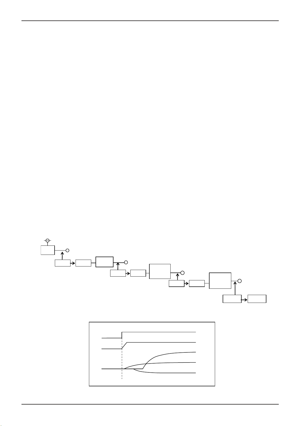
・Starting sequence
For malfunction prevention, starting logic control operates so that each output will rise in order of
VDD Vo1 Vo3 Vo2.
V
CC
As shown below, detectors DET1 to DET3 detect that the output on the detection side has reached 90% (typ.) of the set
voltage, and starts the next block.
VCC
Reg
VDD
DET1
CTL1
Step up
DET2
Vo1
CTL2
Negative
Charge
Pump
DET3
Vo3
CTL3
Positive
Charge
Pump
Vo2
DET4 CLT4
Starting sequence model
0
0
0
5V
2.5V
Vcc
VDD
Vo2
Vo1
Vo3
Fig. 26 Starting Timing Chart
www.rohm.com
© 2010 ROHM Co., Ltd. All rights reserved.
9/21
2010.12 - Rev.
A
BD8163EFV
●Selecting Application Components
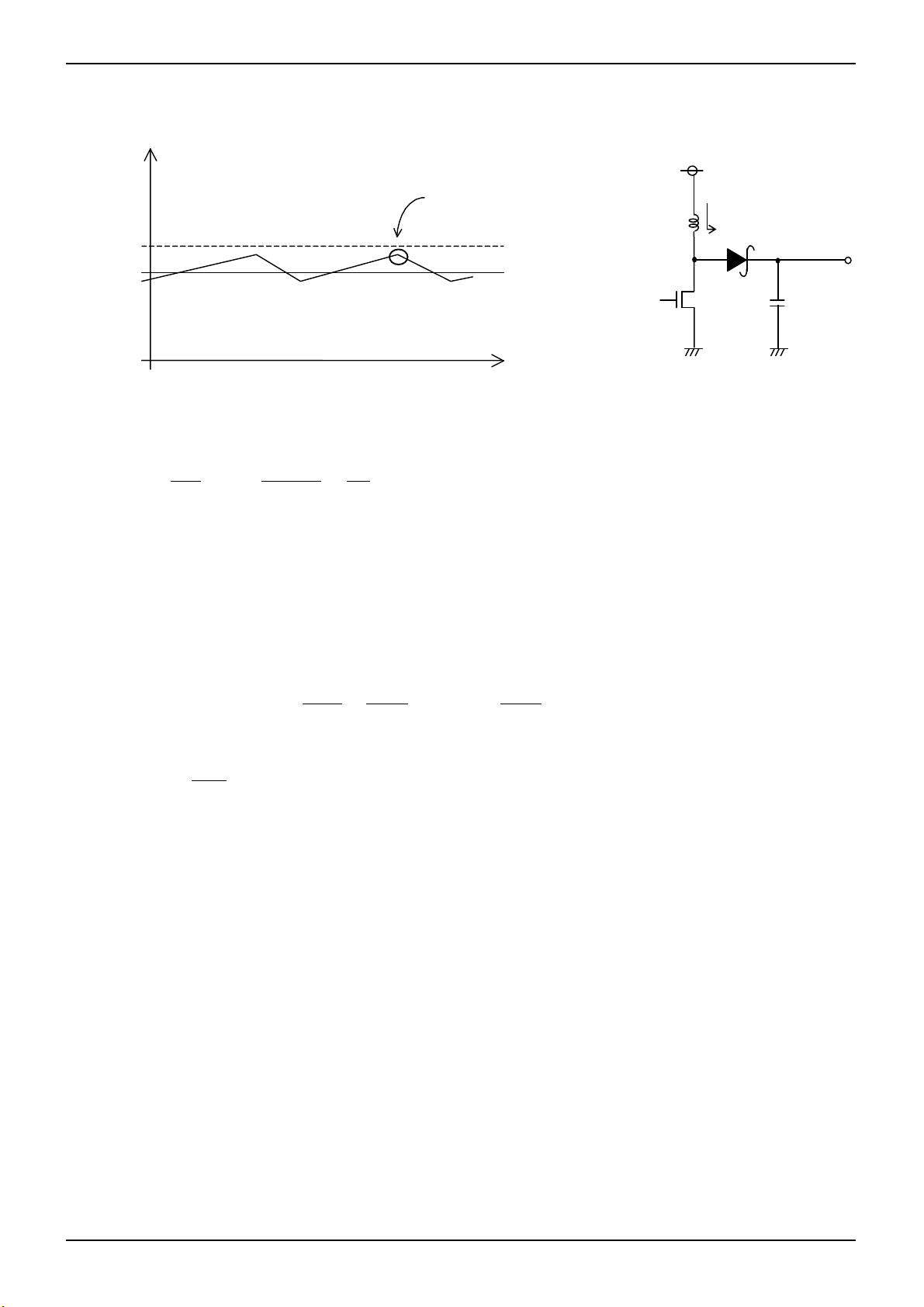
(1) Setting the Output L Constant
The coil to use for output is decided by the rating current I
IL
Fig. 27 Coil Current Waveform
Adjust so that I
+∆IL do not reach the rating current value ILR. At this time, ∆IL can be obtained by the following
INMAX
equation.
ΔI
1
=
L
Vcc
L Vcc f
Vo-Vcc
Set with sufficient margin because the coil value may have the dispersion of 30%. If the coil current exceeds the rating
current I
of the coil, it may damage the IC internal element.
LR
BD8163EFV uses the current mode DC/DC converter control and has the optimized design at the coil value. A coil
inductance (L) of 4.7 µH to 15 µH is recommended from viewpoints of electric power efficiency, response, and stability.
(2) Output Capacity Settings
For the capacitor to use for the output, select the capacitor which has the larger value in the ripple voltage V
value and the drop voltage allowance value at the time of sudden load change. Output ripple voltage is decided by the
following equation.
ΔVPP
= I
LMAX
R
ESR +
Perform setting so that the voltage is within the allowable ripple voltage range.
For the drop voltage during sudden load change; V
V
DR
ΔI
=
Co
10 µs [V]
However, 10 µs is the rough calculation value of the DC/DC response speed. Please set the capacitance considering
the sufficient margin so that these two values are within the standard value range.
(3) Selecting the Input Capacitor
Since the peak current flows between the input and output at the DC/DC converter, a capacitor is required to install at
the input side. For the reason, the low ESR capacitor is recommended as an input capacitor which has the value more
than 10 µF and less than 100 mΩ. If a capacitor out of this range is selected, the excessive ripple voltage is superposed
on the input voltage; accordingly it may cause the malfunction of IC.
However these conditions may vary according to the load current, input voltage, output voltage, inductance and
switching frequency. Be sure to perform the margin check using the actual product.
and input current maximum value I
LR
I
INMAX + ∆IL should not reach
the rating value level
ILR
I
INMAX
average current
1
1
fCo Vo 2
[A] Here, f is the switching frequency.
Vcc
(I
LMAX
, please perform the rough calculation by the following equation.
DR
-
ΔI
Technical Note
of the coil.
INMAX
VCC
L
L
Fig. 28 Output Application Circuit Diagram
L
[V] Here, f is the switching frequency.
)
I
Vo
Co
allowance
PP
www.rohm.com
© 2010 ROHM Co., Ltd. All rights reserved.
10/21
2010.12 - Rev.

A
BD8163EFV
A
A
(4) Setting RC, CC of the Phase Compensation Circuit
In the current mode control, since the coil current is controlled, a pole (phase lag) made by the CR filter composed of the
output capacitor and load resistor will be created in the low frequency range, and a zero (phase lead) by the output
capacitor and ESR of capacitor will be created in the high frequency range. In this case, to cancel the pole of the power
amplifier, it is easy to compensate by adding the zero point with C
the illustration.
Open loop gain characteristics
Gain
[dB]
0
0
Phase
[deg]
-90
fp(Min)
OUT
l
Min
fp(Max)
OUT
l
Max
Error amp phase
compensation characteristics
Gain
[dB]
Phase
[deg]
0
0
-90
Fig. 29 Gain vs Phase
L
COMP
Vcc,PVcc
SW
GND,PGND
V
CC
Cin
Rc
Cc
Fig. 30 Application Circuit Diagram
It is possible to realize the stable feedback loop by canceling the pole fp(Min.), which is created by the output capacitor
and load resistor, with CR zero compensation of the error amp as shown below.
fz(Amp.) = fp(Min.)
1
2 Rc Cc 2 Romax Co
=
fz(ESR)
ESR
Co
Technical Note
and RC to the output from the error amp as shown in
C
1
Fp =
2 RO C
1
fz(ESR) =
2 E
SR
CO
Pole at the power amplification stage
When the output current reduces, the load resistance
increases and the pole frequency lowers.
R
o
fp(Min) =
2 R
1
OMax
CO
1
fz(Max) =
Zero at the power amplification stage
2 R
OMin
CO
When the output capacitor is set larger, the pole
frequency lowers but the zero frequency will not
change. (This is because the capacitor ESR becomes
1/2 when the capacitor becomes 2 times.)
1
fp(Amp.) =
2 Rc Cc
Vo
Ro
1
[Hz]
[Hz]
O
[Hz]
[Hz] at light load
[Hz] at heavy load
[Hz]
www.rohm.com
© 2010 ROHM Co., Ltd. All rights reserved.
11/21
2010.12 - Rev.
A
BD8163EFV
(Open)
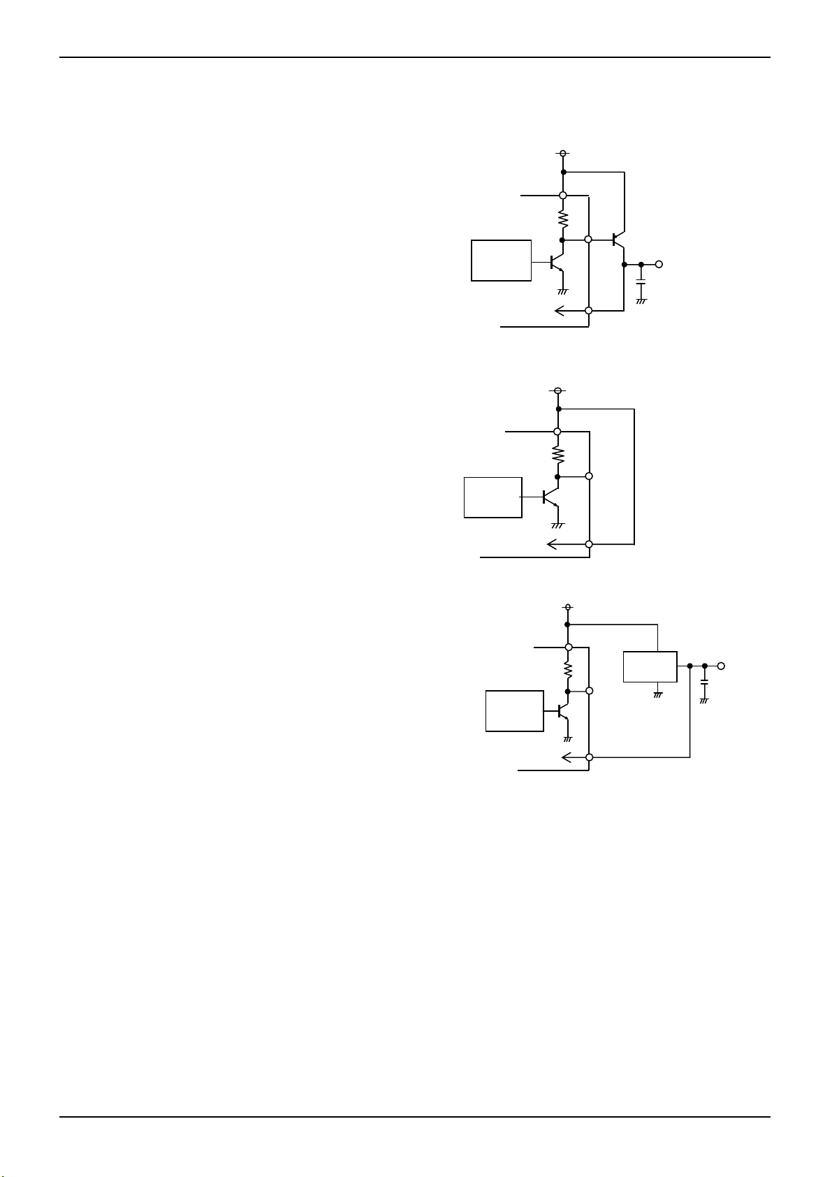
(5) Regulator Controller Settings
The IC incorporates a 2.5 V regulator controller, and a regulator can be formed by using an external PNP transistor.
Design the current capability of the regulator with a margin according to the following formula.
I
= 7mA hfe [A]
OMAX
The hfe is the current gain of the external PNP transistor.
7 mA is the sinking current of the internal transistor.
It is not necessary to use the regulator if the input voltage
is 2.5 V. In that case, input 2.5 V to both VCC and VDD.
When incorporating a regulator into the external
transistor, input the output voltage into the regulator.
Regulator
controller
IC
Regulator
controller
To inside
IC
Regulator
controller
To inside
To inside
IC
VCC=5 V
VCC
Fig.31
2.5 V
VCC
Fig.32
5 V
VCC
Fig.33
VDD
Base
VDD
Base
VDD
Technical Note
2.5 V
VDD=
Ceramic capacitor
with a capacity of
4.7 F or over
3 pin
regulator
Voltage other
than 2.5 V
www.rohm.com
© 2010 ROHM Co., Ltd. All rights reserved.
12/21
2010.12 - Rev.
A
BD8163EFV
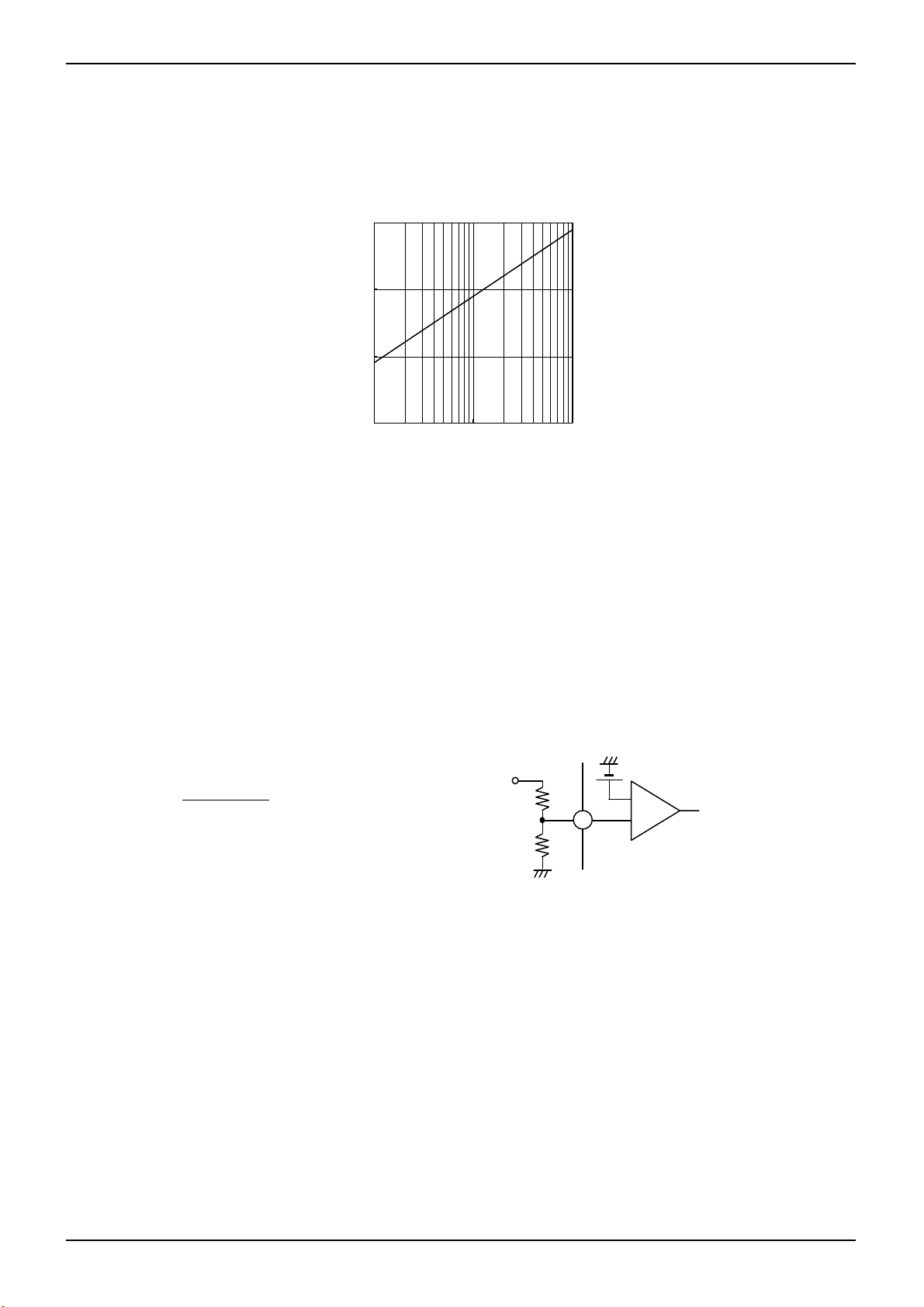
(6) Setting the Soft Start Time
Soft start is required to prevent the coil current at the time of start from increasing and the overshoot of the output
voltage at the starting time. The relation between the capacity and soft start time is shown in the following figure. Refer
to the figure and set capacity C1. Soft start is required to prevent the coil current at the time of start from increasing and
the overshoot of the output voltage at the starting time. Fig. 34 shows the relation between the capacitance and soft start
time. Please refer to it to set the capacitance.
As the capacitance, 0.001 µF to 0.1 µF is recommended. If the capacitance is set lower than 0.001 µF, the overshooting
may occur on the output voltage. If the capacitance is set larger than 0.1µF, the excessive back current flow may occur
in the internal parasitic elements when the power is turned OFF and it may damage IC. When there is the activation
relation (sequences) with other power supplies, be sure to use the high accuracy product (such as X5R). Soft start time
may vary according to the input voltage, loads, coils and output capacity. Be sure to verify the operation using the actual
product.
(7) Design of the Feedback Resistor Constant
Refer to the following equation to set the feedback resistor. As the setting range, 10 kΩto 330 kΩis recommended. If
the resistor is set lower than a 10 kΩ, it causes the reduction of power efficiency. If it is set more than 330 kΩ, the offset
voltage becomes larger by the input bias current 0.4 µA(Typ.) in the internal error amplifier.
Vo =
R8 + R9
R9
1.24 [V]
10
1
0.1
DELAY TIME[ms]
0.01
0.001 0.01 0.1
SS CAPACITANC E[uF ]
Fig. 34 SS Pin Capacitance vs Delay Time
Sep-up
Vo
R8
7
R9
FB1
Fig. 35
Technical Note
Reference voltage 1.24 V
+
ERR
-
www.rohm.com
© 2010 ROHM Co., Ltd. All rights reserved.
13/21
2010.12 - Rev.

A
BD8163EFV
(8) Positive-side Charge Pump Settings
The IC incorporates a charge pump controller, thus making it possible to generate stable gate voltage.
The output voltage is determined by the following formula. As the setting range, 10 kΩto 330 kΩis recommended. If the
resistor is set lower than a 10kΩ, it causes the reduction of power efficiency. If it is set more than 330 kΩ, the offset
voltage becomes larger by the input bias current 0.4 µA (Typ.) in the internal error amp.
Vo =
R8 + R9
R9
In order to prevent output voltage overshooting, add capacitor C8 in parallel with R8. The recommended capacitance is
1000 pF to 4700 pF. If a capacitor outside this range is inserted, the output voltage may oscillate.
By connecting capacitance to the DLS, a rising delay time can be set for the positive-side charge pump.
The delay time is determined by the following formula.
Delay time of charge pump block t
= ( C
t
DELAY
where, C
is the external capacitance.
DLS
(9) Negative-side Charge Pump Settings
This IC incorporates a charge pump controller for negative voltage, thus making it possible to generate stable gate
voltage. The output voltage is determined by the following formula. As the setting range, 10 k Ω to 330 k Ω is
recommended. If the resistor is set lower than a 10 kΩ, it causes the reduction of power efficiency. If it is set more than
330 kΩ, the offset voltage becomes larger by the input bias current 0.4 µA (Typ.) in the internal error amp.
Vo3 = -
R6
R7
The delay time is internally fixed at 200 µs.
In order to prevent output voltage overshooting, insert capacitor C6 in parallel with R6. The recommended capacitance
is 1000 pF to 4700 pF. If a capacitor outside this range is inserted, the output voltage may oscillate.
1.24 [V]
0.6 )/5 µA [s6]
DLS
1.04 + 0.2 V [V]
C8
1000 pF to 4700 pF
DELAY
1000 pF to 4700 pF
Vo2
C6
R8
R9
Vo3
12
Fig. 36
R6
R7
Technical Note
Reference voltage 1.24 V
+
ERR
-
FB2
0.2 V
-
23
FB3
24
REF
Fig.37
ERR
+
1.24 V
www.rohm.com
© 2010 ROHM Co., Ltd. All rights reserved.
14/21
2010.12 - Rev.

A
BD8163EFV
●Gate Shading Setting Method
The IG input signal allows the high-level and low-level control of the positive-side gate voltage. The slope of output can be
set by the external RC. The recommended resistance set value is 200 Ωto 5.1 kΩand the recommended capacitor set
value is 0.001 µF to 0.1 µF. The aggravation of efficiency may be caused if settings outside this range are made.
Determine ∆V by referring to the following value. The following calculation formula is used for ∆V.
tWH
Fig. 38
tWL
CR
Limits
) ) [V]
Unit Condition
TIMING STANDARD VALUE
Parameter Symbol
ΔV = Vo2GS ( 1 - exp ( -
IG
tWL
tLH
Vo2GS
ΔV
Min. Typ. Max.
Technical Note
H
L
H
L
IG “L” Time tWL 1 2 - µs -
IG “H” Time tWH 1 18 - µs -
Vo2GS “H” to “L Voltage difference ΔV - 10 - V TWL = 2 µs, R = 500Ω*
Vo2GS “L” to “H” Time tLH - 0.1 - µs ∆V = 10 V *
IG
IC
Gate
Shading
Control
Fig. 39
From positive-side pump
Vo2
Vo2GS
C
R
GSOUT
Gate driver
www.rohm.com
© 2010 ROHM Co., Ltd. All rights reserved.
15/21
2010.12 - Rev.

A
BD8163EFV
●Application Examples
Although we are confident that the application circuit diagram reflects the best possible recommendations, be sure to verify
circuit characteristics for your particular application. When a circuit is used modifying the externally connected circuit
constant, be sure to decide allowing sufficient margins considering the dispersion of values by external parts as well as our
IC including not only the static but also the transient characteristic. For the patent, we have not acquired the sufficient
confirmation. Please acknowledge the status.
(a) Input voltage
5 V
(b) Input voltage
2.5 V
Vo3
REF
VDD
Vo3
REF
Vo2GS
Vo2
Fig. 40
VDD
Fig. 41
Technical Note
Vo1
Vo2GS
Vo2
Vo1
www.rohm.com
© 2010 ROHM Co., Ltd. All rights reserved.
16/21
2010.12 - Rev.

A
BD8163EFV
(c) When Inserting PMOS Switch
Vo3
REF
VDD
Technical Note
Vo2GS
Vo2
Vo1
Fig. 42
www.rohm.com
© 2010 ROHM Co., Ltd. All rights reserved.
17/21
2010.12 - Rev.

A
BD8163EFV
Technical Note
●I/O Equivalent Circuits
2.VDD 3.BASE 5.DLS,8.SS
VCC
120kΩ
30kΩ
VCC
VDD
6.COMP 7.FB1,12.FB2 10.SW
VDD
VDD
VDD
11.IG 13.Vo2 14.Vo2GS
VDD
200KΩ
VDD
Vo2
Vo2
15.GSOUT 16.C2H,19.C1H 17.C2L,18.C1L,21.C3
23.FB3 24.REF
Vo2
VDD
VDD
Vo1
VDD
Vo1
www.rohm.com
© 2010 ROHM Co., Ltd. All rights reserved.
Fig. 43
18/21
2010.12 - Rev.

A
BD8163EFV
Technical Note
●Power Dissipation Reduction
1200
1000
1100mW
On 70 mm × 70 mm × 1.6 mm
Glass-epoxy PCB
800
600
400
200
Power Dissipation : Pd (mW)
0
0 25 50 75 100 125 150
Ambient Temperature: Ta
(℃)
Fig.44
●Notes for use
1) Absolute maximum ratings
Use of the IC in excess of absolute maximum ratings such as the applied voltage or operating temperature range may
result in IC damage. Assumptions should not be made regarding the state of the IC (short mode or open mode) when such
damage is suffered. A physical safety measure such as a fuse should be implemented when use of the IC in a special
mode where the absolute maximum ratings may be exceeded is anticipated.
2) GND potential
Ensure a minimum GND pin potential in all operating conditions.
3) Setting of heat
Use a thermal design that allows for a sufficient margin in light of the power dissipation (Pd) in actual operating conditions.
4) Pin short and mistake fitting
Use caution when orienting and positioning the IC for mounting on printed circuit boards. Improper mounting may result in
damage to the IC. Shorts between output pins or between output pins and the power supply and GND pins caused by the
presence of a foreign object may result in damage to the IC.
5) Actions in strong magnetic field
Use caution when using the IC in the presence of a strong magnetic field as doing so may cause the IC to malfunction.
6) Testing on application boards
When testing the IC on an application board, connecting a capacitor to a pin with low impedance subjects the IC to stress.
Always discharge capacitors after each process or step. Ground the IC during assembly steps as an antistatic measure,
and use similar caution when transporting or storing the IC. Always turn the IC's power supply off before connecting it to or
removing it from a jig or fixture during the inspection process.
7) Ground wiring patterns
When using both small signal and large current GND patterns, it is recommended to isolate the two ground patterns,
placing a single ground point at the application's reference point so that the pattern wiring resistance and voltage
variations caused by large currents do not cause variations in the small signal ground voltage. Be careful not to change the
GND wiring patterns of any external components.
www.rohm.com
© 2010 ROHM Co., Ltd. All rights reserved.
19/21
2010.12 - Rev.

A
BD8163EFV
(
)
(
)
(
)
(
)
Technical Note
8) This monolithic IC contains P+ isolation and P substrate layers between adjacent elements in order to keep them isolated.
P/N junctions are formed at the intersection of these P layers with the N layers of other elements to create a variety of
parasitic elements. For example, when the resistors and transistors are connected to the pins as shown in Fig.45, a
parasitic diode or a transistor operates by inversing the pin voltage and GND voltage. The formation of parasitic elements
as a result of the relationships of the potentials of different pins is an inevitable result of the IC's architecture. The
operation of parasitic elements can cause interference with circuit operation as well as IC malfunction and damage. For
these reasons, it is necessary to use caution so that the IC is not used in a way that will trigger the operation of parasitic
elements, such as the application of voltages lower than the GND (P board) voltage to input and output pins.
Pin A
P+
N
P
Resistor
N
P
GND
~
~
P+
Parasitic element
Transistor (NPN)
Pin B
N
C
P+
N
Parasitic elements
B
N
N
P substrate
~
~
E
P
GND
GND
P+
N
Fig.45 Example of a Simple Monolithic IC Architecture
Pin B
Pin A
C
B
~
~
E
GND
Parasitic elements
~
~
Parasitic element
GND
9) Overcurrent protection circuits
An overcurrent protection circuit designed according to the output current is incorporated for the prevention of IC
destruction that may result in the event of load shorting. This protection circuit is effective in preventing damage due to
sudden and unexpected accidents. However, the IC should not be used in applications characterized by the continuous
operation or transitioning of the protection circuits. At the time of thermal designing, keep in mind that the current capability
has negative characteristics to temperatures.
10) Thermal shutdown circuit
This IC incorporates a built-in thermal shutdown circuit for the protection from thermal destruction. The IC should be used
within the specified power dissipation range. However, in the event that the IC continues to be operated in excess of its
power dissipation limits, the attendant rise in the chip's temperature Tj will trigger the thermal shutdown circuit to turn off all
output power elements. The circuit automatically resets once the chip's temperature Tj drops.
Operation of the thermal shutdown circuit presumes that the IC's absolute maximum ratings have been exceeded.
Application designs should never make use of the thermal shutdown circuit.
11) Testing on application boards
At the time of inspection of the installation boards, when the capacitor is connected to the pin with low impedance, be sure
to discharge electricity per process because it may load stresses to the IC. Always turn the IC's power supply off before
connecting it to or removing it from a jig or fixture during the inspection process. Ground the IC during assembly steps as
an antistatic measure, and use similar caution when transporting or storing the IC.
www.rohm.com
© 2010 ROHM Co., Ltd. All rights reserved.
20/21
2010.12 - Rev.
A
BD8163EFV
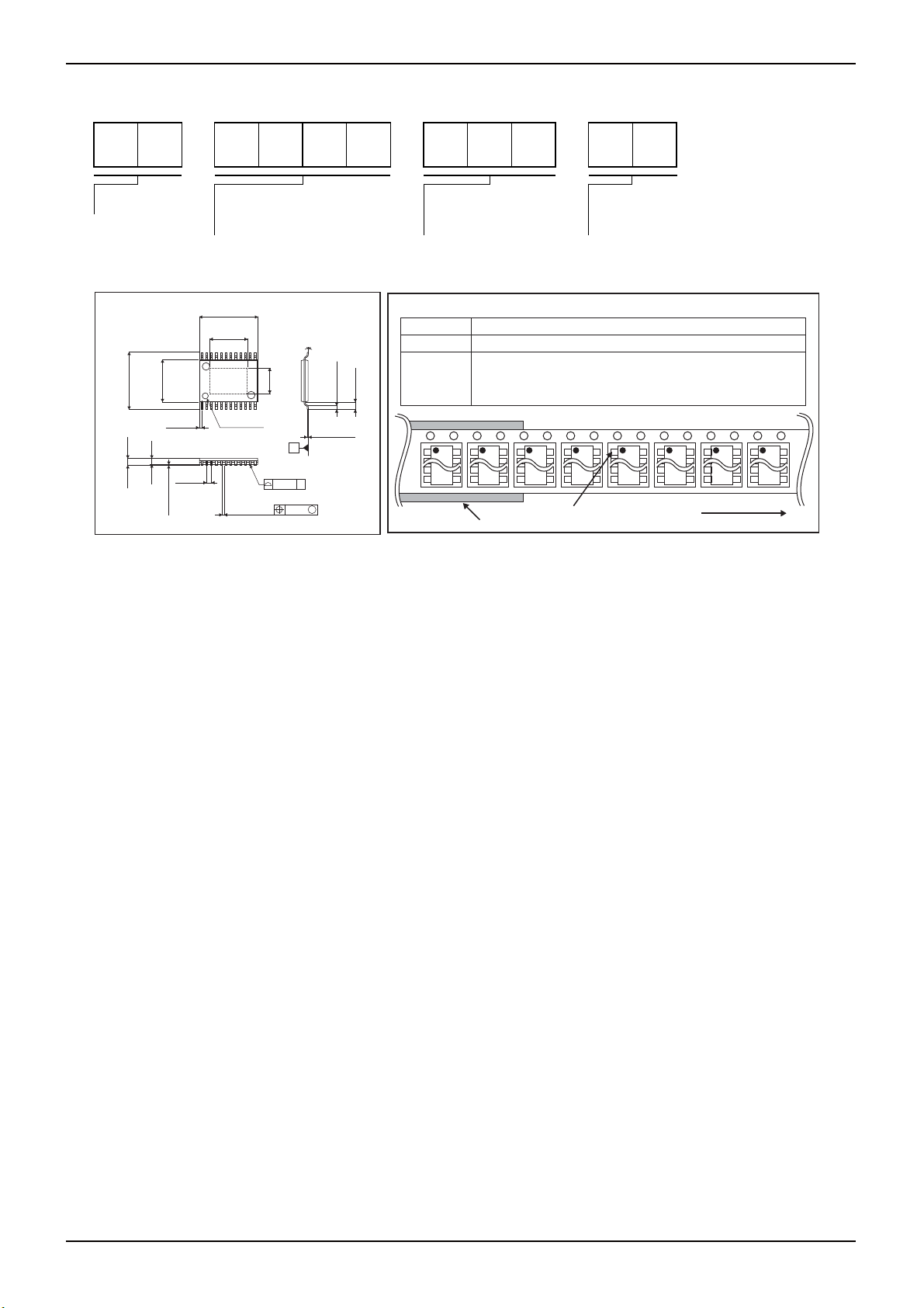
●Ordering part number
Technical Note
B
D 8 1 6 3 E F V - E 2
Part No. Part No. Package
HTSSOP-B24
7.6±0.2
5.6±0.1
0.325
1.0MAX
0.85±0.05
0.08±0.05
7.8±0.1
(MAX 8.15 include BURR)
(5.0)
24 13
112
1PIN MARK
0.65
+0.05
0.24
-
0.04
0.08
(3.4)
S
0.08
4°
S
M
+
6°
−
4°
0.53±0.15
+0.05
0.17
-
0.03
(Unit : mm)
1.0±0.2
<Tape and Reel information>
EFV: HTSSOP-B24
Embossed carrier tape (with dry pack)Tape
Quantity
Direction
of feed
2000pcs
E2
The direction is the 1pin of product is at the upper left when you hold
()
reel on the left hand and you pull out the tape on the right hand
Reel
Packaging and forming specification
E2: Embossed tape and reel
1pin
Order quantity needs to be multiple of the minimum quantity.
∗
Direction of feed
www.rohm.com
© 2010 ROHM Co., Ltd. All rights reserved.
21/21
2010.12 - Rev.

Notes
No copying or reproduction of this document, in par t or in whole, is permitted without the
consent of ROHM Co.,Ltd.
The content specied herein is subject to change for improvement without notice.
The content specied herein is for the purpose of introducing ROHM's products (hereinafter
"Products"). If you wish to use any such Product, please be sure to refer to the specications,
which can be obtained from ROHM upon request.
Examples of application circuits, circuit constants and any other information contained herein
illustrate the standard usage and operations of the Products. The peripheral conditions must
be taken into account when designing circuits for mass production.
Great care was taken in ensuring the accuracy of the information specied in this document.
However, should you incur any damage arising from any inaccuracy or misprint of such
information, ROHM shall bear no responsibility for such damage.
The technical information specied herein is intended only to show the typical functions of and
examples of application circuits for the Products. ROHM does not grant you, explicitly or
implicitly, any license to use or exercise intellectual property or other rights held by ROHM and
other parties. ROHM shall bear no responsibility whatsoever for any dispute arising from the
use of such technical information.
Notice
The Products specied in this document are intended to be used with general-use electronic
equipment or devices (such as audio visual equipment, ofce-automation equipment, communication devices, electronic appliances and amusement devices).
The Products specied in this document are not designed to be radiation tolerant.
While ROHM always makes efforts to enhance the quality and reliability of its Products, a
Product may fail or malfunction for a variety of reasons.
Please be sure to implement in your equipment using the Products safety measures to guard
against the possibility of physical injury, re or any other damage caused in the event of the
failure of any Product, such as derating, redundancy, re control and fail-safe designs. ROHM
shall bear no responsibility whatsoever for your use of any Product outside of the prescribed
scope or not in accordance with the instruction manual.
The Products are not designed or manufactured to be used with any equipment, device or
system which requires an extremely high level of reliability the failure or malfunction of which
may result in a direct threat to human life or create a risk of human injur y (such as a medical
instrument, transportation equipment, aerospace machinery, nuclear-reactor controller, fuelcontroller or other safety device). ROHM shall bear no responsibility in any way for use of any
of the Products for the above special purposes. If a Product is intended to be used for any
such special purpose, please contact a ROHM sales representative before purchasing.
If you intend to export or ship overseas any Product or technology specied herein that may
be controlled under the Foreign Exchange and the Foreign Trade Law, you will be required to
obtain a license or permit under the Law.
Thank you for your accessing to ROHM product informations.
More detail product informations and catalogs are available, please contact us.
ROHM Customer Support System
www.rohm.com
© 2010 ROHM Co., Ltd. All rights reserved.
http://www.rohm.com/contact/
R1010
A
 Loading...