

Page 1
Power Supply IC Series for TFT LCD Panels
High-precision
Gamma Correction IC with built-in DAC
BD8143MUV
●Description
This gamma correction voltage generation IC feature built-in DACs and provide a 1chip solution with setting control via serial
communications, a high-precision 10-bitDAC, and Buffer Amp (12ch).
●Features
1) 1chip design means fewer components
2) Built-in 10bit DAC
3) DAC output Buffer AMP (12ch)
4) Amp input select (CTL)
5) 3-line serial interface control
6) Thermal shut down
7) Power ON Reset Circuit
8) VQFN032V5050 Package
●Applications
These ICs can be used with TFT LCD Panels used by Large-Screen and High-Definition LCD TVs.
●Absolute maximum ratings (Ta=25℃)
Parameter Symbol Limit Unit
Power Supply Voltage 1 DVCC 7 V
Power Supply Voltage 2 VCC 20 V
REFIN Voltage REF 20 V
Amplifier Drive Current Io 30 *
Junction Temperature Tjmax 150 ℃
Power Dissipation Pd 2440 *2 mW
Operating Temperature Range Topr -40~+105 ℃
Storage Temperature Range Tstg -55~+150 ℃
*1 Pd, should not be exceeded.
*2 Reduced by 19.52mW/°C over 25°C, when mounted on a glass epoxy board.
(4-layer 74.2×74.2×1.6mm).
●Operating Condition (Ta=-40℃~105℃)
Parameter Symbol
Power Supply Voltage 1 DVCC 2.3 5.5 V
Power Supply Voltage 2 VCC 8 18 V
REFIN Voltage REF 8 18 V
AMP0 Drive Current IOA -40 - mA
AMP1~10 Drive Current IOB -20 20 mA
AMP11 Drive Current IOC - 40 mA
Serial CLK Frequency fCLK - 5 MHz
OSC Frequency FOSC - 200 kHz
MIN MAX
1
mA
Limit
Unit
No.09035EBT08
www.rohm.com
© 2009 ROHM Co., Ltd. All rights reserved.
1/10
2009.07 - Rev.B
Page 2
BD8143MUV
●Electrical Characteristics (Unless otherwise specified, Ta=25℃,DVCC=3.3V,VCC=15V)
Parameter Symbol
〔REFIN〕
Sink Current Iref 90 200 µA REF=10V
〔γCORRECTION AMP〕
Source Drive Current (AMP0) IooA -60 mA DAC=7V,OUT0=13V
Source Drive Current (AMP1~10) IooB -30 mA DAC=3.5V,OUT1~10=0V
Source Drive Current (AMP11) IooC -10 mA DAC=0.5V,OUT11=0V
Sink Drive Current (AMP0) IoiA 10 mA DAC=7V,OUT0=15V
Sink Drive Current (AMP1~10) IoiB 30 mA DAC=3.5V,OUT1~10=15V
Sink Drive Current (AMP11) IoiC 60 mA DAC=0.5V,OUT11=2V
Load regulation (OUT0) ⊿V-A 10 mV Io=0mA~-35mA, OUTx=6V
Load regulation (OUT1~10) ⊿V-B 10 mV Io=-15mA~15mA, OUTx=6V
Load regulation (OUT11) ⊿V-C 10 mV Io=0mA~35mA, OUTx=6V
Slew Rate SR 3 V/µs
OUT Voltage High (OUT0) VOH-A VCC-0.4 VCC-0.15 - V Io=-35mA
OUT Voltage High (OUT1~10) VOH-B VCC-0.75 - V Io=-15mA
OUT Voltage High (OUT11) VOH-C VCC-0.75 - V Io=-15mA
OUT Voltage Low (OUT0) VOL-A - 0.75 V Io=15mA
OUT Voltage Low (OUT1~10) VOL-B - 0.75 V Io=15mA
OUT Voltage Low (OUT11) VOL-C - 0.1 0.2 V Io=35mA
〔DAC〕
Resolution Coding Res 10 Bit
Non-Linear Error (INL) LE -2 - 2 LSB
Differential Error (DNL) DLE -2 - 2 LSB
〔OSC〕
OSC Frequency fosc - 100 - kHz Internal oscillator mode
〔CONTROL SIGNAL〕
Sink Current Ictl 16.5 µA VIN=3.3V
Threshold Voltage VTH DVCC×0.2 DVCC×0.8 V
〔CONTROL〕
OUT0 Voltage Vpre0 -
OUT1 Voltage Vpre1 -
OUT2 Voltage Vpre2 -
OUT3 Voltage Vpre3 -
OUT4 Voltage Vpre4 -
OUT5 Voltage Vpre5 -
OUT6 Voltage Vpre6 -
OUT7 Voltage Vpre7 -
OUT8 Voltage Vpre8 -
OUT9 Voltage Vpre9 -
OUT10 Voltage Vpre10 -
OUT11 Voltage Vpre11 -
〔WHOLE DEVICE〕
VDAC Detection Voltage Vdet 2.6 3.2 3.6 V
Circuit Current ICC 5 mA CTL=”LOW”
This product is not designed for protection against radio active rays.
MIN TYP MAX
Limit
REFIN
X 12/13
REFIN
X 11/13
REFIN
X 10/13
REFIN
X 9/13
REFIN
X 813
REFIN
X 7/13
REFIN
X 6/13
REFIN
X 5/13
REFIN
X 4/13
REFIN
X 3/13
REFIN
X 2/13
REFIN
X 1/13
Unit Conditions
Error with ideal straight Range
00A~3F5
Error with ideal amount of
Increase in 1LSB Range
00A~3F5
- V CTL=”LOW”
- V CTL=”LOW”
- V CTL=”LOW”
- V CTL=”LOW”
- V CTL=”LOW”
- V CTL=”LOW”
- V CTL=”LOW”
- V CTL=”LOW”
- V CTL=”LOW”
- V CTL=”LOW”
- V CTL=”LOW”
- V CTL=”LOW”
Technical Note
www.rohm.com
© 2009 ROHM Co., Ltd. All rights reserved.
2/10
2009.07 - Rev.B
Page 3
K
C
8
A
5
C
N
C
C
0
9
BD8143MUV
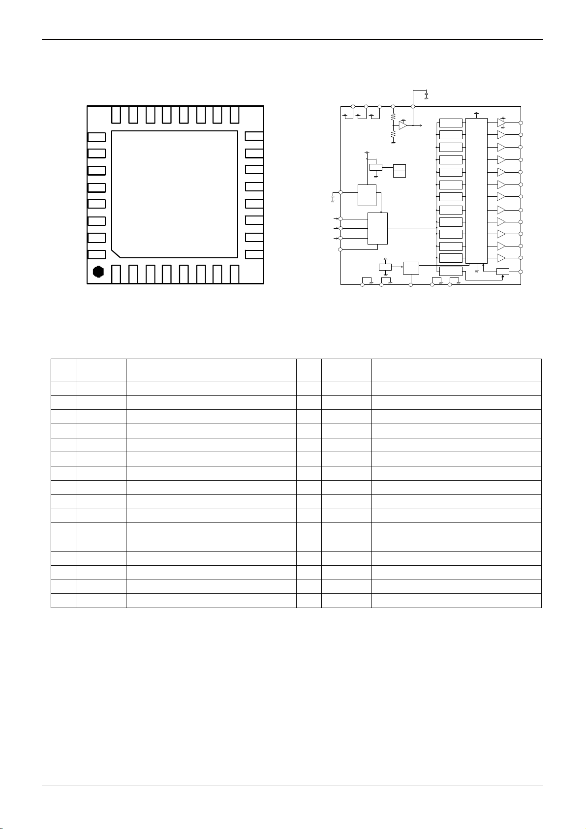
●Pin No ●Block Diagram
OUT
OUT1
OUT11
VC
REFI
VDA
DACGND
N.
OUT
OUT7
24 23 22 21 19 17 18 20
25
26
27
28
29
30
31
32
1 2 3 4 6 8 7 5
SDIN
LATCH
OUT6
CL
GND AGND
SDOUT
OUT3
OUT4
OUT
16
OUT2
15
OUT1
14
OUT0
13
VCC
N.C
12
CTL
11
10
N.C
OS C
9
CT
DVC
N.C
GND
LATCH
DATA
CLK
SDOUT
VDD
VCC REFIN
VDD
VREF
CT
Power
ON
Reset
Serial
DACGND GND OSC AGND AGND
VDAC
VCC
VCC
R
R
I/F
VDD
OSC
UVLO
VDAC
REG
TSD
Refresh
Control
Fig.1 Pin No. & Block Diagram
●Pin NO. & Function Table
PIN
No.
Pin
Name
Function
PIN
No.
Pin
Name
1 LATCH LATCH signal input 17 OUT3 Gamma 3 output
2 SDIN DATA signal input 18 OUT4 Gamma 4 output
3 CLK CLK signal input 19 OUT5 Gamma 5 output
4 SDOUT DATA signal output 20 AGND Ground for Buffer AMP
5 DVCC Digital Power Supply 21 AGND Ground for Buffer AMP
6 CT Capacitor connection for Power on Reset 22 OUT6 Gamma 6 output
7 GND Ground 23 OUT7 Gamma 7 output
8 N.C - 24 OUT8 Gamma 8 output
9 OSC DAC Synchronized clock inout 25 OUT9 Gamma 9 output
10 N.C - 26 OUT10 Gamma 10 output
11 CTL Output control signal input 27 OUT11 Gamma 11 output
12 N.C - 28 VCC Power Supply for Buffer AMP
13 VCC Power Supply for Buffer AMP 29 REFIN DAC reference input
14 OUT0 Gamma 0 output 30 VDAC DAC Voltage output
15 OUT1 Gamma 1 output 31 DACGND Ground for DAC
16 OUT2 Gamma 2 output 32 N.C -
Technical Note
VDAC
REGISTER0
REGISTER1
REGISTER2
REGISTER3
REGISTER4
REGISTER5
REGISTER6
REGISTER7
REGISTER8
REGISTER9
REGISTER10
REGISTER11
REGISTER12
Function
DAC
Control
VCC
AMP0
x2
OUT0
AMP1
OUT1
x2
AMP2
x2
OUT2
AMP3
x2
OUT3
AMP4
OUT4
x2
AMP5
x2
OUT5
AMP6
OUT6
x2
AMP7
x2
OUT7
AMP8
OUT8
x2
AMP9
OUT9
x2
AMP10
x2
OUT10
AMP11
OUT11
x2
CTL
CTL
www.rohm.com
© 2009 ROHM Co., Ltd. All rights reserved.
3/10
2009.07 - Rev.B
Page 4

BD8143MUV
●Block Operation
・REG
REG amplifiers the voltage applied to REFIN by 0.5x and output it to the VDAC pin. Connect a 1µF phase compensation
capacitor to the VDAC pin.
・DAC Control
DAC Control convents the 10-bit digital signal read to the register to a voltage.
・Amp
Amp amplifiers the voltage output from DAC Control by 2x. Input includes sample & hold function, refreshed by OSC.
・OSC
The OSC generates the frequency that determines the Amp's refresh time.
External input can be selected using serial input.
・Power On Reset
When the digital power supply DVCC is activated, each IC generates a reset signal to initialize the serial interface, registers.
Adding a 1,000 pF capacitor to the CT pin ensures that reset operation can be performed reliably, without regard to the
speed with which the power supply starts up.
・VREF
This block generates the internal reference voltage.
・TSD(Thermal Shut Down)
The TSD circuit turns output off when the chip temperature reaches or exceeds approximately 175°C(TYP) in order to
prevent thermal destruction or thermal runaway. When the chip returns to a specified temperature, the circuit resets.
The TSD circuit is designed only to protect the IC itself. Application thermal design should ensure operation of the IC
below the thermal shutdown junction temperature of approximately 150°C(TYP).
・CTL
CTL signal can select Amp input. If CTL=”L”, each output voltage is fixed at REFIN voltage divided 13th equality.
IF CTL=”H”, each Amp input connect DAC output, and each output comply with each register.
・Register
A serial signal (consisting of 10-bit gamma correction voltage values) input using the serial interface is held for each
register address. Data is initialized by the reset signal generated during a power-on reset.
・Serial I/F
The serial interface uses a 3-line serial data format (LATCH, CLK, SDIN). It is used to set gamma correction voltages,
specify register addresses, and select OSC I/O.
Technical Note
www.rohm.com
© 2009 ROHM Co., Ltd. All rights reserved.
4/10
2009.07 - Rev.B
Page 5

BD8143MUV
Technical Note
●Serial Communication
The serial data control block is composed of Shift-Register, DAC Register and DAC circuit.
The DAC register memorizes data from the serial interface (LATCH, CLK and SDIN).
The DAC circuit makes control voltage from the register output and it outputs to the each block. The DAC register value turns
back the preset value when Power Supply starts up.
Then, beginning 1bit of SDIN is always 0, because it is for test. Next 1bit switches OSC mode.
If input 0, OSC mode is internal mode (the frequency is 100kHz). If input 1, it is external one that require external clock.
LATCH
CLK
SDIN
CLOCK
CONTROL
SERIAL DATA CONTROL BLOCK
d13
d14
d15
d16
d12
Shift Register
d11
d10
d9
d8
d7
d6
d5
d4
d3
d2
d1
d0
OUT0~12
Register
10bit
ADDRESS
DECORDE
5bit
OSC
MODE
1bit
TEST
MODE
1bit
DAC
Fig.2 SERIAL BLOCK
①TIMING OF SERIAL COMMUNICATION
The 17 bits Serial data from SDIN terminal is loaded to Shift-Register at the rise edge of CLK, and these data is loaded to
DAC Register at the rise edge of LATCH.
If serial data period is less than 17 bits while LATCH state is LOW, the serial data is not memorized. If serial data period is
more than 17 bits while LATCH state is LOW, last 17 bits are effective.
LATCH
CLK
d0 d1 d2 d3 d4 d5 d6 d7 d8 d9 d10
SDIN
TIMING OF SERIAL COMMUNICATION
d1
1
d12
d14 d15
d16
d13
Fig.3 TIMING OF SERIAL COMMUNICATION
②SERIAL DATA
The composition of SERIAL DATA INPUT(SDIN)
First → → Last
d0 d1 d2 d3 d4 d5 d6 d7 d8 d9 d10 d11 d12 d13 d14 d15 d16
0 X Resister Address DATA
REGISTER NAME
ADDRESS
d2 d3 d4 d5 d6 d7~d16
FUNCTION
PRESET VALUE
Register 0 0 0 0 0 0 OUT0 Voltage of control 00 0000 0000
Register 1 0 0 0 0 1 OUT1 Voltage of control 00 0000 0000
Register 2 0 0 0 1 0 OUT2 Voltage of control 00 0000 0000
Register 3 0 0 0 1 1 OUT3 Voltage of control 00 0000 0000
Register 4 0 0 1 0 0 OUT4 Voltage of control 00 0000 0000
Register 5 0 0 1 0 1 OUT5 Voltage of control 00 0000 0000
Register 6 0 0 1 1 0 OUT6 Voltage of control 00 0000 0000
Register 7 0 0 1 1 1 OUT7 Voltage of control 00 0000 0000
Register 8 0 1 0 0 0 OUT8 Voltage of control 00 0000 0000
Register 9 0 1 0 0 1 OUT9 Voltage of control 00 0000 0000
Register 10 0 1 0 1 0 OUT10 Voltage of control 00 0000 0000
Register 11 0 1 0 1 1 OUT11 Voltage of control 00 0000 0000
Register 12(*) 0 1 1 0 0 - 00 0000 0000
(*)IF Register 12 is loaded at DATA=1010100000(2A0h), each output comply with each register regardless of CTL signal.
www.rohm.com
© 2009 ROHM Co., Ltd. All rights reserved.
5/10
2009.07 - Rev.B
Page 6

BD8143MUV
●Serial Communication Timing Chart
LATCH
CLK
SDIN
tLC
tSC
tWL tWH
tCL
tLA
Technical Note
Fig.4
●Timing Standard Value
Parameter Symbol
Min. Typ. Max.
LIMIT
Unit
LATCH Set up time tLC 0.1 - - us
SDIN Set up time tSC 0.1 - - us
CLK “H” time tWH 0.1 - - us
CLK “L” time tWL 0.1 - - us
LATCH hold time tCL 0.1 - - us
LATCH “H” time tLA 0.6 - - us
●Setting γ-Correction
Formula (1) shows the relationship between γ output voltage (OUT0~OUT11) and DAC digital value.
Output Voltage(OUT0~OUT11)=({(DAC digital value +1)/1024}×(REFIN/2)‐10mV)×2.0025 ・・・(1)
●Power Supply Sequence
Digital power supply DVCC must be supplied earlier than VCC for the prevent of wrong behavior.
The serial data must be input after cancellation of “Power on Reset”.
When turn off power supply, VCC must be done earlier than DVCC.
VCC
REFIN
DVCC
LATCH
CLK
SDIN
・・・
・・・
・・・
・・・
tDS
・・・
・・・
tSV
・・・
tVcc
・・・
tVR
・・・
・・・
・・・
・・・
tVD
tRV
Fig.5 Power Supply Sequence
●Power Supply Sequence Standard Value
Parameter Symbol
Min. Typ. Max.
LIMIT
Unit Condition
Timing of serial data input tDS 100 - - μs Cct=1000pF
Timing of VCC ON tSV - 10 - μs
Timing of REFIN ON tVR 0 10 - μs
Timing of REFIN OFF tRV 0 10 - μs
Timing of VCC OFF tVD 0 10 - μs
VCC rise time tVCC 1 - - ms
www.rohm.com
© 2009 ROHM Co., Ltd. All rights reserved.
6/10
2009.07 - Rev.B
Page 7

BD8143MUV
Technical Note
●Data writing time for register
Data writing time for register depend on frequency of CLK. Below formula shows data writing time for all registers.
(Because data writing time for a register is needed at 17bit data + LATCH “H” time.)
18 CLK × ×12ch [µs]
f
CLK
1
[MHz]
●Refresh time of Amp input
Each Amp input have sample & hold function refreshed by OSC frequency (fosc).
Below formula shows refresh cycle.
×12ch [µs]
f
OSC
1
[kHz]
When internal OSC mode, f
=100kHz (Typ).
OSC
●Function of selecting Amp input
This IC can select Amp input by CTL signal. If CTL=”L”, Amp input is connected to resistance division of REFIN voltage.
IF CTL=”H”, connected to DAC output. When VCC(REFIN) supplies with CTL=”L”, it is possible to start up without opposite
Voltage of each output. Then, if the CTL signal changes “H” after 1ms and over since VCC(REFIN) supplied and data send
finished, start up sequence should be below Fig.
(*Amp input is connected to DAC output not only by CTL=”H”, but also DATA=1010100000(2A0h) sended to Register 12.
Also in this case, please send DATA=1010100000(2A0h) to Register 12 after 1ms and over since VCC(REFIN) supplied
And output data send finished, at this time CTL=”L”.)
REFIN
VCC
Preset value
CTL
VDAC
VCC
DAC
Control
x2
OUT
DAC value
CTL
Preset value DAC value
Fig.6 Selecting Amp input block diagram Fig.7 Start up sequence
OUT0
OUT1
OUT2
OUT10
OUT11
www.rohm.com
© 2009 ROHM Co., Ltd. All rights reserved.
7/10
2009.07 - Rev.B
Page 8

BD8143MUV
●Input Output Circuit (BD8143MUV)
1.LATCH
2.SDIN 3.CLK
DVCC
Technical Note
4.SDOUT 6.CT
DVCC
DVCC
GND
GND
9.OSC 11. CTL
DVCC
GND
29.REFIN
DVCC
GND
30.VDAC
VCC
VCC
AGND
AGND
Fig.8
GND
14.OUT0 15.OUT1 16.OUT2
17.OUT3 18.OUT4 19.OUT5
22.OUT6 23.OUT7 24.OUT8
25.OUT9 26.OUT10 27.OUT11
VCC
AGND
www.rohm.com
© 2009 ROHM Co., Ltd. All rights reserved.
8/10
2009.07 - Rev.B
Page 9

BD8143MUV
(
)
(
)
(
)
Technical Note
●Notes for use
1) Absolute maximum ratings
Use of the IC in excess of absolute maximum ratings such as the applied voltage or operating temperature range may
result in IC damage. Assumptions should not be made regarding the state of the IC (short mode or open mode) when such
damage is suffered. A physical safety measure such as a fuse should be implemented when use of the IC in a special
mode where the absolute maximum ratings may be exceeded is anticipated.
2) GND potential
Ensure a minimum GND pin potential in all operating conditions.
3) Setting of heat
Use a thermal design that allows for a sufficient margin in light of the power dissipation (Pd) in actual operating conditions.
4) Pin short and mistake fitting
Use caution when orienting and positioning the IC for mounting on printed circuit boards. Improper mounting may result in
damage to the IC. Shorts between output pins or between output pins and the power supply and GND pins caused by the
presence of a foreign object may result in damage to the IC.
5) Actions in strong magnetic field
Use caution when using the IC in the presence of a strong magnetic field as doing so may cause the IC to malfunction.
6) Testing on application boards
When testing the IC on an application board, connecting a capacitor to a pin with low impedance subjects the IC to stress.
Always discharge capacitors after each process or step. Ground the IC during assembly steps as an antistatic measure,
and use similar caution when transporting or storing the IC. Always turn the IC's power supply off before connecting it to or
removing it from a jig or fixture during the inspection process.
7) Ground wiring patterns
When using both small signal and large current GND patterns, it is recommended to isolate the two ground patterns,
placing a single ground point at the application's reference point so that the pattern wiring resistance and voltage
variations caused by large currents do not cause variations in the small signal ground voltage. Be careful not to change the
GND wiring patterns of any external components.
8) Regarding input pin of the IC
This monolithic IC contains P+ isolation and P substrate layers between adjacent elements in order to keep them isolated.
P/N junctions are formed at the intersection of these P layers with the N layers of other elements to create a variety of
parasitic elements. For example, when the resistors and transistors are connected to the pins as shown in below Fig.9, a
parasitic diode or a transistor operates by inverting the pin voltage and GND voltage. The formation of parasitic elements
as a result of the relationships of the potentials of different pins is an inevitable result of the IC's architecture. The operation
of parasitic elements can cause interference with circuit operation as well as IC malfunction and damage. For these
reasons, it is necessary to use caution so that the IC is not used in a way that will trigger the operation of parasitic elements
such as by the application of voltages lower than the GND (P substrate) voltage to input and output pins.
(Pin A)
N N
P
Fig.9 Example of a Simple Monolithic IC Architecture
Resistor
N
P
GND
~
~
P+P+
Parasitic elements
Pin B
P+
N N
Parasitic elements
Transistor (NPN)
C
B
E
~
~
N
P
N
P substrate
GND
Pin B
C
B
~
~
E
GND
P+
Pin A
GND
Parasitic
elements
Parasitic
elements
~
~
GND
9) Overcurrent protection circuits
An overcurrent protection circuit designed according to the output current is incorporated for the prevention of IC damage
that may result in the event of load shorting. This protection circuit is effective in preventing damage due to sudden and
unexpected accidents. However, the IC should not be used in applications characterized by the continuous operation or
transitioning of the protection circuits. At the time of thermal designing, keep in mind that the current capacity has negative
characteristics to temperatures.
10) Thermal shutdown circuit (TSD)
This IC incorporates a built-in TSD circuit for the protection from thermal destruction. The IC should be used within the
specified power dissipation range. However, in the event that the IC continues to be operated in excess of its power
dissipation limits, the attendant rise in the chip's junction temperature Tj will trigger the TSD circuit to turn off all output power
elements. The circuit automatically resets once the junction temperature Tj drops.Operation of the TSD circuit presumes that
the IC's absolute maximum ratings have been exceeded. Application designs should never make use of the TSD circuit.
11) Testing on application boards
At the time of inspection of the inst
allation boards, when the capacitor is connected to the pin with low impedance, be sure
to discharge electricity per process because it may load stresses to the IC. Always turn the IC's power supply off before
connecting it to or removing it from a jig or fixture during the inspection process. Ground the IC during assembly steps as
an antistatic measure, and use similar caution when transporting or storing the IC.
12) Push Current
This IC may rush current momentary by power supply order or delay, use caution about power supply coupling capacitor,
width or routing of VCC ,GND patterns
www.rohm.com
© 2009 ROHM Co., Ltd. All rights reserved.
9/10
2009.07 - Rev.B
Page 10

BD8143MUV
●Ordering part number
Technical Note
B D 8 1 4 3 M U V - E 2
Part No. Part No.
VQFN032V5050
5.0± 0.1
1.0MAX
0.08 S
C0.2
32
0.4± 0.1
25
0.75
5.0± 0.1
3.4± 0.1
24
0.5
1PIN MARK
+0.03
81
9
16
17
+0.05
0.25
-
0.02
0.04
0.02
-
3.4± 0.1
S
(0.22)
(Unit : mm)
Package
MUV: VQFN032V5050
<Tape and Reel information>
Embossed carrier tapeTape
Quantity
Direction
of feed
2500pcs
E2
The direction is the 1pin of product is at the upper left when you hold
()
reel on the left hand and you pull out the tape on the right hand
Reel
Packaging and forming specification
E2: Embossed tape and reel
1pin
Order quantity needs to be multiple of the minimum quantity.
∗
Direction of feed
www.rohm.com
© 2009 ROHM Co., Ltd. All rights reserved.
10/10
2009.07 - Rev.B
Page 11

Notes
No copying or reproduction of this document, in part or in whole, is permitted without the
consent of ROHM Co.,Ltd.
The content specied herein is subject to change for improvement without notice.
The content specied herein is for the purpose of introducing ROHM's products (hereinaf ter
"Products"). If you wish to use any such Product, please be sure to refer to the specications,
which can be obtained from ROHM upon request.
Examples of application circuits, circuit constants and any other information contained herein
illustrate the standard usage and operations of the Products. The peripheral conditions must
be taken into account when designing circuits for mass production.
Great care was taken in ensuring the accuracy of the information specied in this document.
However, should you incur any damage arising from any inaccuracy or misprint of such
information, ROHM shall bear no responsibility for such damage.
The technical information specied herein is intended only to show the typical functions of and
examples of application circuits for the Products. ROHM does not grant you, explicitly or
implicitly, any license to use or exercise intellectual property or other rights held by ROHM and
other par ties. ROHM shall bear no responsibility whatsoever for any dispute arising from the
use of such technical information.
Notice
The Products specied in this document are intended to be used with general-use electronic
equipment or devices (such as audio visual equipment, ofce-automation equipment, communication devices, electronic appliances and amusement devices).
The Products specied in this document are not designed to be radiation tolerant.
While ROHM always makes ef forts to enhance the quality and reliability of its Products, a
Product may fail or malfunction for a variety of reasons.
Please be sure to implement in your equipment using the Products safety measures to guard
against the possibility of physical injury, re or any other damage caused in the event of the
failure of any Product, such as derating, redundancy, re control and fail-safe designs. ROHM
shall bear no responsibility whatsoever for your use of any Product outside of the prescribed
scope or not in accordance with the instruction manual.
The Products are not designed or manufactured to be used with any equipment, device or
system which requires an extremely high level of reliability the failure or malfunction of which
may result in a direct threat to human life or create a risk of human injur y (such as a medical
instrument, transportation equipment, aerospace machinery, nuclear-reactor controller,
fuel-controller or other safety device). ROHM shall bear no responsibility in any way for use of
any of the Products for the above special purposes. If a Product is intended to be used for any
such special purpose, please contact a ROHM sales representative before purchasing.
If you intend to export or ship overseas any Product or technology specied herein that may
be controlled under the Foreign Exchange and the Foreign Trade Law, you will be required to
obtain a license or permit under the Law.
www.rohm.com
© 2009 ROHM Co., Ltd. All rights reserved.
Thank you for your accessing to ROHM product informations.
More detail product informations and catalogs are available, please contact us.
ROHM Customer Support System
http://www.rohm.com/contact/
R0039
A
 Loading...