


Power Management ICs for Automotive Body Control
White Backlight LED Drivers
for Medium to Large LCD Panels
(Switching Regulator Type)
BD8112EFV-M
●Description
BD8112EFV-M is a white LED driver with the capability of withstanding high input voltage (36V MAX). This driver has
2ch constant-current drivers integrated in 1-chip, which each channel can draw up to 150mA max, so that high brightness
LED driving can be realized. Furthermore, a current-mode buck-boost DC/DC controller is also integrated to achieve stable
operation against voltage input and also to remove the constraint of the number of LEDs in series connection.
The brightness can be controlled by either PWM or VDAC techniques.
●Features
1) Input voltage range 5.0 -30 V
2) Integrated buck-boost current-mode DC/DC controller
3) Two integrated LED current driver channels (150 mA max. each channel)
4) PWM Light Modulation (Minimum Pulse Width 25µs)
5) Oscillation frequency accuracy ±5%
6) Built-in protection functions (UVLO, OVP, TSD, OCP, SCP)
7) LED abnormal status detection function (OPEN/ SHORT)
8) HTSSOP-B24 package
●Applications
Backlight for display audio, small type panels, etc.
●Absolute maximum ratings (Ta=25℃)
Parameter Symbol Ratings Unit
Power supply voltage VCC 36 V
No.11039ECT11
BOOT , OUTH Voltage V
SW, CS Voltage V
BOOT-SW Voltage V
LED output voltage V
VREG, OVP, OUTL, FAIL1, FAIL2,
LEDEN, ISET, VDAC, PWM, SS, COMP,
RT, SYNC, EN voltage
Power Consumption Pd 1.10 *1 W
Operating temperature range Topr -40~+105 ℃
Storage temperature range Tstg -55~+150 ℃
LED maximum output current I
Junction temperature Tjmax 150 ℃
*1 IC mounted on glass epoxy board measuring 70mm × 70mm × 1.6mm, power dissipated at a rate of 8.8mw/℃ at temperatures above 25℃.
*2 Dispersion figures for LED maximum output current and VF are correlated. Please refer to data on separate sheet.
*3 Amount of current per channel.
V
VREG, VOVP, VOUTL, VFAIL1, VFAI L2 ,
V
LEDEN, VISET, VVDAC, VPWM, VSS, VCOMP,
BOOT, VOUTH
SW, VCS
BOOT-SW
LED1,2
V
RT, VSYNC, VEN
41 V
36 V
7 V
36 V
-0.3~7 < V
150
LED
V
CC
*2 *3
mA
www.rohm.com
© 2010 ROHM Co., Ltd. All rights reserved.
1/22
2011.08 - Rev.C

BD8112EFV-M
●Operating conditions (Ta=25℃)
Parameter Symbol Limits Unit
Power supply voltage VCC 5.0~30 V
Technical Note
Oscillating frequency range F
External synchronization
frequency range
*4 *5
External synchronization
pulse duty range
*4 Connect SYNC to GND or OPEN when not using external frequency synchronization.
*5 Do not switch between internal and external synchronization when an external synchronization signal is input to the device.
250~600 kHz
OSC
F
fosc~600 kHz
SYNC
40~60 %
F
SDUTY
●Electrical characteristics (Unless otherwise specified, VCC=12V Ta=25℃)
Parameter Symbol
Min Typ Max.
Circuit current ICC - 7 14 mA
Limits
Unit Conditions
EN=Hi, SYNC=Hi, RT=OPEN
PWM=Low, ISET=OPEN, C
Standby current IST - 4 8 µA EN=Low
[VREG Block (VREG)]
Reference voltage V
4.5 5 5.5 V I
REG
REG
[OUTH Block]
OUTH high-side ON resistance R
1.5 3.5 7.0 Ω ION=-10mA
ONHH
=-5mA, C
REG
=2.2µF
=10µF
IN
OUTH low-side ON resistance R
Over-current protection
operating voltage
V
[OUTL Block]
OUTL high-side ON resistance R
OUTL low –side ON resistance R
[SW Block]
SW low -side ON resistance R
[Error Amplifie Block]
LED voltage V
COMP sink current I
COMP source current I
COMPSINK
COMPSOURCE
[Oscillator Block]
Oscillating frequency F
1.0 2.5 5.0 Ω ION=10mA
ONHL
V
V
OLIMIT
ONLH
ONLL
ON_SW
LED
-0.66
2.0 4.0 8.0 Ω ION=-10mA
1.0 2.5 5.0 Ω ION=10mA
2.0 4.5 9.0 Ω I
0.9 1.0 1.1 V
CC
CC
-0.6
VCC
-0.54
V
ON_SW
15 25 35 µA V
-35 -25 -15 µA V
285 300 315 KHz RT=100kΩ
OSC
=10mA
=2V, Vcomp=1V
LED
=0V, Vcomp=1V
LED
◎This product is not designed for use in radioactive environments.
www.rohm.com
© 2010 ROHM Co., Ltd. All rights reserved.
2/22
2011.08 - Rev.C

BD8112EFV-M
Parameter Symbol
[OVP Block]
Over-voltage detection
reference voltage
Limits
Min Typ Max.
V
1.9 2.0 2.1 V V
OVP
Technical Note
Unit Conditions
=Sweep up
OVP
OVP hysteresis width V
SCP Latch OFF Delay Time T
0.45 0.55 0.65 V V
OHYS
70 100 130 ms RT=100kΩ
SCP
[UVLO Block ]
UVLO voltage V
UVLO hysteresis width V
4.0 4.3 4.6 V VCC : Sweep down
UVLO
50 150 250 mV VCC : Sweep up
UHYS
[LED Output Block]
LED current
relative dispersion width
LED current
absolute dispersion width
ISET voltage V
-3 - +3 %
△I
LED1
△I
-5 - +5 %
LED2
1.96 2.0 2.04 V R
ISET
PWM minimum pulse width Tmin 25 - - µs F
PWM maximum duty Dmax - - 100 % F
PWM frequency F
- - 20 KHz Duty=50%, I
PWM
=Sweep down
OVP
=50mA,
I
LED
=(I
ΔI
LED1
I
=50mA,
LED
ΔI
=(I
LED2
=120kΩ
ISET
=150Hz, I
PWM
=150Hz, I
PWM
LED/ILED_AVG
/50mA-1)×100
LED
=50mA
LED
=50mA
LED
=50mA
LED
-1)×100
=0~2V, R
V
VDAC gain G
Open detection voltage V
LED Short detection Voltage V
LED Short Latch OFF Delay Time T
PWM Latch OFF Delay Time T
- 25 - mA/V
VDAC
0.2 0.3 0.4 V V
OPEN
4.2 4.5 4.8 V V
SHORT
70 100 130 ms RT=100kΩ
SHORT
70 100 130 ms RT=100kΩ
PWM
DAC
=VDAC÷R
I
LED
= Sweep down
LED
= Sweep up
OVP
[Logic Inputs (EN, SYNC, PWM, LEDEN)]
Input HIGH voltage V
Input LOW voltage V
Input current 1 IIN 20 35 50 µA
2.1 - 5.5 V
INH
GND - 0.8 V
INL
V
=5V
IN
(SYNC, PWM, LEDEN)
Input current 2 IEN 15 25 35 µA VEN=5V (EN)
[FAIL Output (open drain) ]
=120kΩ
ISET
×Gain
ISET
FAIL LOW voltage VOL - 0.1 0.2 V IOL=0.1mA
◎This product is not designed for use in radioactive environments.
www.rohm.com
© 2010 ROHM Co., Ltd. All rights reserved.
3/22
2011.08 - Rev.C

BD8112EFV-M
●Electrical characteristic curves (Reference data) (Unless otherwise specified, Ta=25℃)
5.5
5.3
5.1
Vcc= 12V
400
Vcc= 12V
360
320
4.9
280
4.7
OUT PUT VOLTAGE:VREG [V]
4.5
-40 - 15 10 35 60 85
TEM PERATU RE:Ta [℃]
Fig.1 VREG temperature
characteristic
240
Fig.3 OSC 温度特性
SWITCHING FREQUENCY:FOSC [kHz]
200
-40 - 15 10 35 60 85
TEMPERATURE:Ta [℃]
Fig.2 OSC temperature
characteristic
55
50
53
51
49
47
OUTPUTCURRENT :ILED [mA]
45
Vcc= 12V
-40 - 15 10 35 60 85
TEMPER ATUR E:Ta [℃]
Fig.4 ILED temperature
characteristic
40
30
20
10
OUTPUTCURRENT :ILED [mA]
0
0 0.5 1 1.5 2
VDAC VOLTAGE:VD AC[V]
Fig.5 VDAC Gain① Fig.6 VDAC Gain②
100
85
70
55
EFFIC IENCY [%]
40
VCC=30V
100
85
VCC=12V
70
55
EFFICIENCY [%]
40
25
50 100 150 200 250
Total_Io [mA]
Fig.7 Efficiency
(LED2 Parallel 5 step)
0.66
0.64
0.62
0.60
0.58
0.56
OUT PUT VOLTAGE:Vcc-Vcs [V]
0.54
-40 - 15 10 35 60 85
TEMPER ATUR E:Ta [℃]
Fig.10 Overcurrent detecting voltage
temperature characteristic
VCC=12V
25
50 100 150 200 250
OUTPUT CURRENT [mA]
Fig.8 Efficiency
(LED2 Parallel 7 step)
10
8
6
4
2
OUT PUT VOLTAGE:VREG [V]
0
012345
EN VOLTAGE:VEN [V]
Fig.11 EN threshold voltage
Technical Note
400
360
Vcc= 12V
320
280
240
SWITCHING FREQUENCY:FOSC [kHz]
200
-40 - 15 10 35 60 85
TEM PERATU RE:Ta [℃]
Fig.3 ILED depend on VLED
5
4
3
2
1
OUTPU TCURR ENT :ILED [mA]
0
0 0.02 0.04 0.06 0.08 0.1
VDAC VOLTAGE:VDAC [V]
6.0
4.0
2.0
OUTPUT CARRENT:Icc [mA]
0.0
0 6 12 18 24 30 36
10
8
6
4
2
OUTPUTCURRENT :ILED [mA]
0
01 23 45
Fig.12 PWM threshold voltage
Vcc=12V
SUPPLY VOLTAGE:Vcc [V]
Fig.9 Circuit Current
(Switching OFF)
PWM VOLT AGE:VEN [V]
www.rohm.com
© 2010 ROHM Co., Ltd. All rights reserved.
4/22
2011.08 - Rev.C

BD8112EFV-M
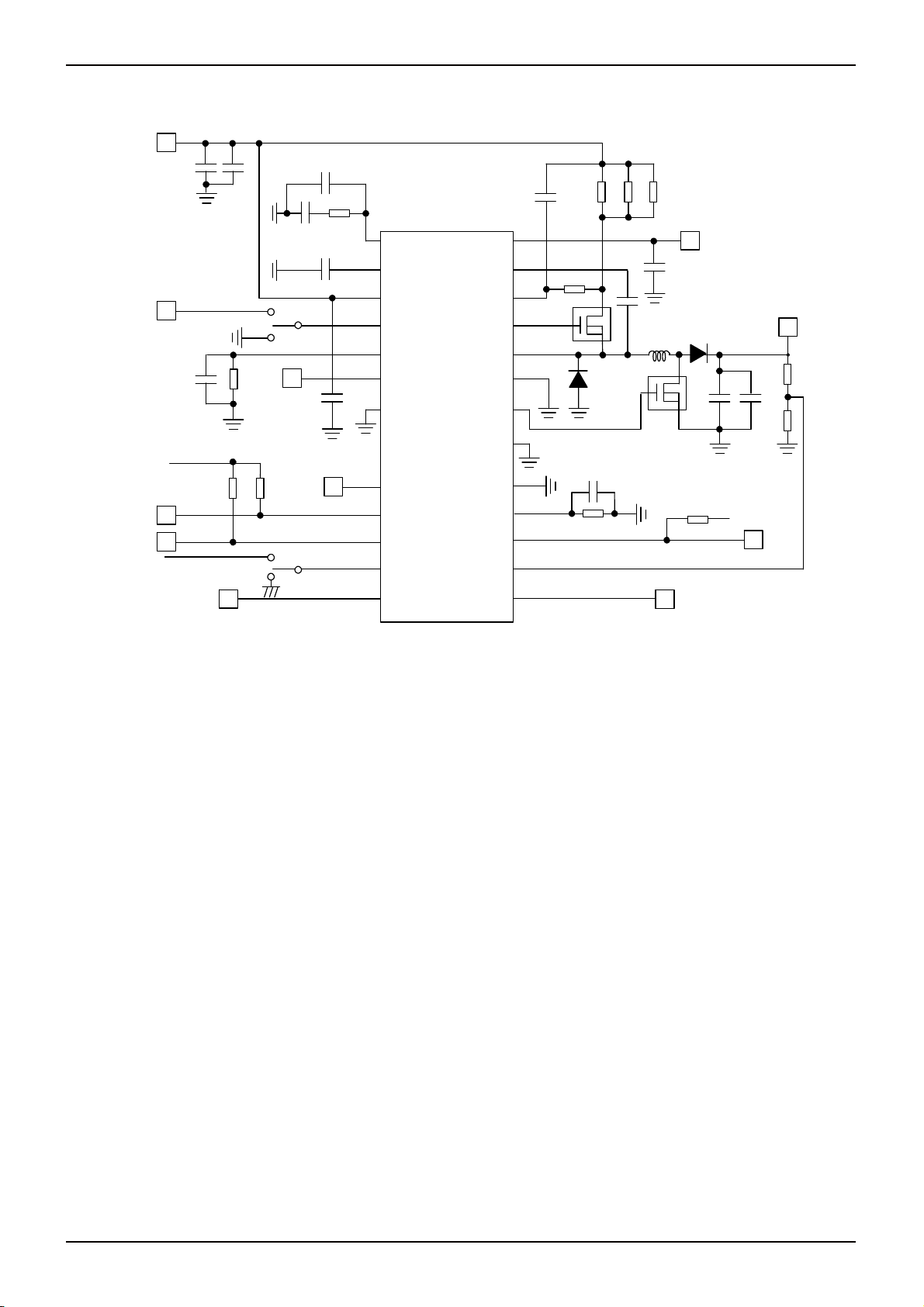
●Block diagram and pin configuration
Vin
Ccomp
CRT
C
RISET
IN
RT
C
C
VREG
VCC
EN
SYNC
RT
COMP
R
PC
PC
SS
SS
PWM
VDAC
ISET
VREG
OCP OVP
PWM
OSC
SS
UVLO TSD
SLOPE
ISET
Timer
Latch
Control Logic
Open Short Detect
OVP
-
PWM
+
ERR AMP
Current driver
Timer
Latch
LEDEN
Fig.13
-
-
+
Open Det
Short Det
OCP
DRV
CTL
Technical Note
C
OUT
OVP
+
-
VREG
CS
FAIL1
BOOT
OUTH
SW
DGND
OUTL
GND
LED1
LED2
PGND
FAIL2
www.rohm.com
© 2010 ROHM Co., Ltd. All rights reserved.
5/22
2011.08 - Rev.C

BD8112EFV-M
●Pin layout
BD8112EFV-M(HTSSOP-B24)
●Pin function table
Pin Symbol Function
COMP
SS
VCC
EN
RT
SYNC
GND
PWM
FAIL1
FAIL2
LEDEN
LED1
10
11
12
Technical Note
1
2
3
4
5
6
7
8
9
Fig.14
24
23
22
21
20
19
18
17
16
15
14
13
VREG
BOOT
CS
OUTH
SW
DGND
OUTL
PGND
ISET
VDAC
OVP
LED2
1 COMP Error amplifier output
2 SS Soft start time-setting capacitance input
3 VCC Input power supply
4 EN Enable input
5 RT Oscillation frequency-setting resistance input
6 SYNC External synchronization signal input
7 GND Small-signal GND
8 PWM PWM light modulation input
9 FAIL1 Failure signal output
10 FAIL2 LED open/short detection signal output
11 LEDEN LED output enable pin
12 LED1 LED output 1
13 LED2 LED output 2
14 OVP Over-voltage detection input
15 VDAC DC variable light modulation input
16 ISET LED output current-setting resistance input
17 PGND LED output GND
18 OUTL Low-side external MOSFET Gate Drive out put
19 DGND Low-side internal MOSFET Source out put
20 SW High-side external MOSFET Source pin
21 OUTH High-side external MOSFET Gate Drive out pin
22 CS DC/DC Current Sense Pin
23 BOOT High-side MOSFET Power Supply pin
24 VREG Internal reference voltage output
www.rohm.com
© 2010 ROHM Co., Ltd. All rights reserved.
6/22
2011.08 - Rev.C

BD8112EFV-M
Technical Note
●5V voltage reference (VREG)
5V (Typ.) is generated from the VCC input voltage when the enable pin is set high. This voltage is used to power internal
circuitry, as well as the voltage source for device pins that need to be fixed to a logical HIGH. UVLO protection is integrated
into the VREG pin. The voltage regulation circuitry operates uninterrupted for output voltages higher than 4.45 V (Typ.),
but if output voltage drops to 4.3 V (Typ.) or lower, UVLO engages and turns the IC off. Connect a capacitor (Creg = 2.2µF
Typ.) to the VREG terminal for phase compensation. Operation may become unstable if Creg is not connected.
●Constant-current LED drivers
If less than four constant-current drivers are used, unused channels should be switched off via the LEDEN pin configuration.
The truth table for these pins is shown below. If a driver output is enabled but not used (i.e. left open), the IC’s open
circuit-detection circuitry will operate. Please keep the unused pins open. The LEDEN terminals are pulled down internally
in the IC, so if left open, the IC will recognize them as logic LO. However, they should be connected directly to VREG or
fixed to a logic HI when in use.
LED
LED EN
1 2
L ON ON
H ON OFF
・Output current setting
LED current is computed via the following equation:
= min[VDAC , VISET(=2.0V)] / RSET x GAIN [A]
I
LED
(min[VDAC , 2.0V] = the smaller value of either VDAC or VISET; GAIN = set by internal circuitry.)
In applications where an external signal is used for output current control, a control voltage in the range of 0.0 to 2.0 V
can be connected on the VDAC pin to control according to the above equation. If an external control signal is not used,
connect the VDAC pin to VREG (do not leave the pin open as this may cause the IC to malfunction). Also, do not switch
individual channels on or off via the LEDEN pin while operating in PWM mode.
The following diagram illustrates the relation between ILED and GAIN.
3150
ILED vs GAIN
GAIN
3100
3050
3000
2950
2900
2850
0 20 40 60 80 100 120 140 160
ILED[mA]
In PWM intensity control mode, the ON/OFF state of each current driver is controlled directly by the input signal on the
PWM pin; thus, the duty ratio of the input signal on the PWM pin equals the duty ratio of the LED current. When not
controlling intensity via PWM, fix the PWM terminal to a high voltage (100%). Output light intensity is greatest at 100%
input.
PWM
PWM
ILED(50mA/div)
ILED
PWM=150Hz Duty=0.
PWM=150Hz Duty=50%
www.rohm.com
© 2010 ROHM Co., Ltd. All rights reserved.
7/22
2011.08 - Rev.C

BD8112EFV-M
Technical Note
●Buck-Boost DC/DC controller
・Number of LEDs in series connection
Output voltage of the DCDC converter is controlled such that the forward voltage over each of the LEDs on the output is
set to 1.0V (Typ.). DCDC operation is performed only when the LED output is operating. When two or more LED outputs
are operating simultaneously, the LED voltage output is held at 1.0V (Typ.) per LED over the column of LEDs with the
highest VF value. The voltages of other LED outputs are increased only in relation to the fluctuation of voltage over this
column. Consideration should be given to the change in power dissipation due to variations in VF of the LEDs. Please
determine the allowable maximum VF variance of the total LEDs in series by using the description as shown below:
VF variation allowable voltage 3.7V (Typ.) = short detecting voltage 4.5V (Typ.)-LED control voltage 1.0V (Typ.)
The number of LEDs that can be connected in series is limited due to the open-circuit protection circuit, which engages at
85% of the set OVP voltage. Therefore, the maximum output voltage of the under normal operation becomes
30.6 V (= 36 V x 0.85, where (30.6 V – 1.0 V) / VF > N [maximum number of LEDs in series]).
・Over-voltage protection circuit (OVP)
The output of the DCDC converter should be connected to the OVP pin via a voltage divider. In determining an
appropriate trigger voltage of for OVP function, consider the total number of LEDs in series and the maximum variation in
VF. Also, bear in mind that over-current protection (OCP) is triggered at 0.85 x OVP trigger voltage. If the OVP
function engages, it will not release unless the DCDC voltage drops to 72.5% of the OVP trigger voltage. For example, if
ROVP1 (output voltage side), ROVP2 (GND side), and DCDC voltages VOUT are conditions for OVP, then:
VOUT ≥ (ROVP1 + ROVP2) / ROVP2 x 2.0 V.
OVP will engage when VOUT ≧ 32 V if ROVP1 = 330 kΩ and ROVP2 = 22 kΩ.
・Buck-boost DC/DC converter oscillation frequency (FOSC)
The regulator’s internal triangular wave oscillation frequency can be set via a resistor connected to the RT pin (pin 5).
This resistor determines the charge/discharge current to the internal capacitor, thereby changing the oscillating frequency.
Refer to the following theoretical formula when setting RT:
30 x 10
fosc = x α [kHz]
6
(V/A/S) is a constant (±5%) determined by the internal circuitry, and α is a correction factor that varies in relation
30 × 10
RT [Ω]
6
to RT:
{ RT: α = 50kΩ: 0.94, 60kΩ: 0.985, 70kΩ: 0.99, 80kΩ: 0.994, 90kΩ: 0.996, 100kΩ: 1.0,
150kΩ: 1.01, 200kΩ: 1.02, 300kΩ: 1.03, 400kΩ: 1.04, 500kΩ: 1.045}
A resistor in the range of 47kΩ~523kΩ is recommended. Settings that deviate from the frequency range shown below
may cause switching to stop, and proper operation cannot be guaranteed.
600k
500k
400k
300k
Fr equency [kHz ]
200k
100k
k
0 100 200 300 400 500 600 700 800
RT[kΩ]
Fig.15 RT versus switching frequency
・External DC/DC converter oscillating frequency synchronization (FSYNC)
Do not switch from external to internal oscillation of the DC/DC converter if an external synchronization signal is present
on the SYNC pin. When the signal on the SYNC terminal is switched from high to low, a delay of about 30 µs (typ.)
occurs before the internal oscillation circuitry starts to operate (only the rising edge of the input clock signal on the SYNC
terminal is recognized). Moreover, if external input frequency is less than the internal oscillation frequency, the internal
oscillator will engage after the above-mentioned 30 µs (typ.) delay; thus, does not input a synchronization signal with a
frequency less than the internal oscillation frequency.
www.rohm.com
© 2010 ROHM Co., Ltd. All rights reserved.
8/22
2011.08 - Rev.C
BD8112EFV-M
Technical Note
・Soft Start Function
The soft-start (SS) limits the current and slows the rise-time of the output voltage during the start-up, and hence leads to
prevention of the overshoot of the output voltage and the inrush current.
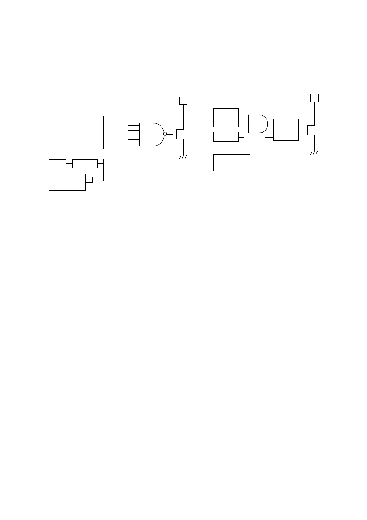
・Self-diagnostic functions
The operating status of the built-in protection circuitry is propagated to FAIL1 and FAIL2 pins (open-drain outputs). FAIL1
becomes low when UVLO, TSD, OVP, or SCP protection is engaged, whereas FAIL2 becomes low when open or short
LED is detected.
UVLO
TSD
OVP
OCP
FAIL1
OPEN
SHORT
MASK
S
Q
R
EN=Low
UVLO/TSD
Counter SCP
S
Q
R
EN=Low
UVLO/TSD
・Operation of the Protection Circuitry
・Under-Voltage Lock Out (UVLO)
The UVLO shuts down all the circuits other than REG when VREG ≦ 4.3V (TYP).
・Thermal Shut Down (TSD)
The TSD shuts down all the circuits other than REG when the Tj reaches 175℃ (TYP), and releases when the Tj
becomes below 150℃ (TYP).
・Over Current Protection (OCP)
The OCP detects the current through the power-FET by monitoring the voltage of the high-side resistor, and activates
when the CS voltage becomes less than VCC-0.6V (TYP).
When the OCP is activated, the external capacitor of the SS pin becomes discharged and the switching operation of
the DCDC turns off.
・Over Voltage Protection (OVP)
The output voltage of the DCDC is detected with the OVP-pin voltage, and the protection activates when the OVP-pin
voltage becomes greater than 2.0V (TYP).
When the OVP is activated, the external capacitor of the SS pin becomes discharged and the switching operation of
the DCDC turns off.
・Short Circuit Protection (SCP)
When the LED-pin voltage becomes less than 0.3V (TYP), the internal counter starts operating and latches off the circuit
approximately after 100ms (when FOSC = 300 kHz). If the LED-pin voltage becomes over 0.3V before 100ms, then the
counter resets. When the LED anode (i.e. DCDC output voltage) is shorted to ground, then the LED current becomes off
and the LED-pin voltage becomes low. Furthermore, the LED current also becomes off when the LED cathode is shorted
to ground. Hence in summary, the SCP works with both cases of the LED anode and the cathode being shorted.
・LED Open Detection
When the LED-pin voltage 0.3V (TYP) as well as OVP-pin voltage 1.7V (TYP) simultaneously, the device detects as
LED open and latches off that particular channel.
FAIL2
www.rohm.com
© 2010 ROHM Co., Ltd. All rights reserved.
9/22
2011.08 - Rev.C

BD8112EFV-M
Technical Note
・LED Short Detection
When the LED-pin voltage 4.5V (TYP) as well as OVP-pin voltage 1.6V (TYP) simultaneously the internal counter
starts operating, and approximately after 100ms (when FOSC = 300 kHz) the only detected channel (as LED short)
latches off. With the PWM brightness control, the detecting operation is processed only when PWM-pin = High. If the
condition of the detection operation is released before 100ms (when FOSC = 300 kHz), then the internal counter resets.
* The counter frequency is the DCDC switching frequency determined by the RT. The latch proceeds at the count of 32770.
Detecting Condition
Protection
Operation after detect
[Detect] [Release]
UVLO VREG<4.3V VREG>4.45V
TSD Tj>175℃ Tj<150℃
All blocks (but except REG)
shut down
All blocks (but except REG)
shut down
OVP VOVP>2.0V VOVP<1.45V SS discharged
OCP VCS≦VCC-0.6V VCS>VCC-0.6V SS discharged
SCP
(100ms delay when FOSC=300kHz)
VLED<0.3V
EN or UVLO
Counter starts and then latches off all
blocks (but except REG)
LED open VLED<0.3V & VOVP>1.7V EN or UVLO The only detected channel latches off
LED short
VLED>4.5V & VOVP<1.6V
(100ms delay when FOSC=300kHz)
EN or UVLO
The only detected channel latches off
(after the counter sets)
www.rohm.com
© 2010 ROHM Co., Ltd. All rights reserved.
10/22
2011.08 - Rev.C

BD8112EFV-M
●Protection Sequence
VCC
*
EN
VREG
UVLO
VDAC
SYNC
PWM
1
4.45V
*
1
*
2
*
2
SS
ILED1
ILED2
ILED1'
ILED2'
VLED1
VLED2
VLED1'
VLED2'
1.0V
VOVP
*
FAIL1
4
<0.3V
1.7V
①
②
>4.5V
100ms
*
3
FAIL2
*1 After VCC voltage reached to operating conditions, set VDAC voltage, and turn on the EN.
After VREG≧4.6V, turn on SYNC and PWM inputs.
*2 Don’t care input sequence PWM and SYNC.
*3 Aprox 100ms of delay when Fosc = 300kHz
*4 When FAIL1 pull-up to outside power supply.
① Case for LED2 in open-mode
When VLED2<0.3V and VOVP>1.7V simultaneously, then LED2 becomes off and FAIL2 becomes low
② Case for LED1’ in short-mode
When VLED1’>4.5V and VOVP<1.6V simultaneously, then LED1’ becomes off after 100ms approx
③ Case for LED2’ in short to GND
③-1 DCDC output voltage increases, and then SS discharges and FAIL1 becomes low
③-2 Detects VLED2’<0.3V and shuts down after 100ms approx
0.3V
2.0V
100ms
③
Technical Note
④
*
3
www.rohm.com
© 2010 ROHM Co., Ltd. All rights reserved.
11/22
2011.08 - Rev.C

BD8112EFV-M
●Procedure for external components selection
Follow the steps as shown below for selecting the external components
1. Work out IL_MAX from the operating conditions.
2. Select the value of RSC such that IOCP > IL_MAX
3. Select the value of L such that 0.05[V/µs] <
4. Select coil, schottky diodes, MOSFET and RCS which meet with the ratings
5. Select the output capacitor which meets with the ripple voltage requirements
6. Select the input capacitor
7. Work on with the compensation circuit
8. Work on with the Over-Voltage Protection (OVP) setting
9. Work on with the soft-start setting
10. erify experimentally
Vout
*RCS < 0.3[V/ µs]
L
Technical Note
Feedback the value of L
www.rohm.com
© 2010 ROHM Co., Ltd. All rights reserved.
12/22
2011.08 - Rev.C

BD8112EFV-M
Technical Note
1. Computation of the Input Peak Current and IL_MAX
①Calculation of the maximum output voltage (Vout_max)
To calculate the Vout_max, it is necessary to take into account of the VF variation and the number of LED connection in
series.
Vout_max = (VF + ΔVF) × N + 1.0V ΔVF: VF Variation N: Number of LED connection in series
②Calculation of the output current Iout
Iout = ILED × 1.05 × M M:Number of LED connection in parallel
③Calculation of the input peak current IL_MAX
IL_MAX = IL_AVG + 1/2ΔIL
IL_AVG = (VIN + Vout) × Iout / (n × VIN)
ΔIL= × × n: efficiency Fosc: switching frequency
VIN
L
1
Fosc
Vout
IN+Vout
V
・The worst case scenario for VIN is when it is at the minimum, and thus the minimum value should be applied in the
equation.
・ The L value of 10µF 47µF is recommended. The current-mode type of DC/DC conversion is adopted for
BD8112EFV-M, which is optimized with the use of the recommended L value in the design stage. This recommendation
is based upon the efficiency as well as the stability. The L values outside this recommended range may cause irregular
switching waveform and hence deteriorate stable operation.
・n (efficiency) is approximately 80%
VIN
Rcs
IL
CS
M1
L
D2
Vout
D1
M2
Co
External Application Circuit
2. The setting of over-current protection
Choose Rcs with the use of the equation Vocp_min (=0.54V) / Rcs > IL_MAX
When investigating the margin, it is worth noting that the L value may vary by approximately ±30%.
3. The selection of the L
In order to achieve stable operation of the current-mode DC/DC converter, we recommend selecting the L value in the
range indicated below:
0.05 [V/µs] < < 0.3 [V/µs]
The smaller allows stability improvement but slows down the response time.
Vout×Rcs
L
Vout×Rcs
L
4. Selection of coil L, diode D1 and D2, MOSFET M1 and M2, and Rcs
Current rating Voltage rating Heat loss
Coil L > IL_MAX ―
Diode D1 > Iocp > VIN_MAX
Diode D2 > Iocp > Vout
MOSFET M1 > Iocp > VIN_MAX
MOSFET M2 > Iocp > Vout
Rcs ― ― > Iocp2 × Rcs
* Allow some margin, such as the tolerance of the external components, when selecting.
* In order to achieve fast switching, choose the MOSFETs with the smaller gate-capacitance.
www.rohm.com
© 2010 ROHM Co., Ltd. All rights reserved.
13/22
2011.08 - Rev.C

BD8112EFV-M
A
Technical Note
5. Selection of the output capacitor
Select the output capacitor Cout based on the requirement of the ripple voltage Vpp.
Vpp = × × + IL_MIN × RESR
Iout
Cout
Vout
Vout+V
IN
1
Fosc
Choose Cout that allows the Vpp to settle within the requirement. Allow some margin also, such as the tolerance of the
external components.
6. Selection of the input capacitor
A capacitor at the input is also required as the peak current flows between the input and the output in DC/DC conversion.
We recommend an input capacitor greater than 10µF with the ESR smaller than 100m. The input capacitor outside of
our recommendation may cause large ripple voltage at the input and hence lead to malfunction.
7. Phase Compensation Guidelines
In general, the negative feedback loop is stable when the following condition is met:
・Overall gain of 1 (0dB) with a phase lag of less than 150º (i.e. a phase margin of 30º or more)
However, as the DC/DC converter constantly samples the switching frequency, the gain-bandwidth (GBW) product of the
entire series should be set to 1/10 the switching frequency of the system. Therefore, the overall stability characteristics
of the application are as follows:
・Overall gain of 1 (0dB) with a phase lag of less than 150º (i.e. a phase margin of 30º or more)
・GBW (frequency at gain 0dB) of 1/10 the switching frequency
Thus, to improve response within the GBW product limits, the switching frequency must be increased.
The key for achieving stability is to place fz near to the GBW.
Vout
Phase-lead fz = [Hz]
Phase-lag fp1 = [Hz]
1
2πCpcRpc
1
2πRLCout
LED
FB
COMP
Good stability would be obtained when the fz is set between 1kHz~10kHz.
In buck-boost applications, Right-Hand-Plane (RHP) Zero exists. This Zero has no gain but a pole characteristic in terms
of phase. As this Zero would cause instability when it is in the control loop, so it is necessary to bring this zero before the
GBW.
fRHP= [Hz] I
Vout+VIN/(Vout+VIN)
2πI
LOAD
L
LOAD: Maximum Load Current
It is important to keep in mind that these are very loose guidelines, and adjustments may have to be made to ensure
stability in the actual circuitry. It is also important to note that stability characteristics can change greatly depending on
factors such as substrate layout and load conditions. Therefore, when designing for mass-production, stability should be
thoroughly investigated and confirmed in the actual physical design.
Rpc
Cpc
www.rohm.com
© 2010 ROHM Co., Ltd. All rights reserved.
14/22
2011.08 - Rev.C
BD8112EFV-M
Technical Note
8. Setting of the over-voltage protection
We recommend setting the over-voltage protection Vovp 1.2V to
1.5V greater than Vout which is adjusted by the number of LEDs
in series connection. Less than 1.2V may cause unexpected
detection of the LED open and short during the PWM brightness
control. For the Vovp greater than 1.5V, the LED short detection
may become invalid.
9. Setting of the soft-start
The soft-start allows minimization of the coil current as well as
Vo
ROVP2
ROVP1
OVP
-
+
2.0V/1.45V
-
+
1.7V/1.6V
the overshoot of the output voltage at the start-up.
For the capacitance we recommend in the range of 0.001 0.1µF. For the capacitance less than 0.001µF may cause
overshoot of the output voltage. For the capacitance greater than 0.1µF may cause massive reverse current through the
parasitic elements of the IC and damage the whole device. In case it is necessary to use the capacitance greater than
0.1µF, ensure to have a reverse current protection diode at the Vcc or a bypass diode placed between the SS-pin and the
Vcc.
Soft-start time TSS
TSS = CSSX0.7V / 5µA [s] CSS: The capacitance at the SS-pin
10.Verification of the operation by taking measurements
The overall characteristic may change by load current, input voltage, output voltage, inductance, load capacitance,
switching frequency, and the PCB layout. We strongly recommend verifying your design by taking the actual
measurements.
www.rohm.com
© 2010 ROHM Co., Ltd. All rights reserved.
15/22
2011.08 - Rev.C

BD8112EFV-M
●Power Dissipation Calculation
Power dissipation can be calculated as follows:
Pc(N) = ICC*VCC + 2*Ciss*VREG*Fsw*Vcc+[VLED*N+△Vf*(N-1)]*ILED
Maximum circuit current
I
CC
V
Supply power voltage
CC
C
External FET capacitance
iss
V
SW gate voltage
sw
F
SW frequency
sw
V
LED control voltage
LED
N LED parallel numeral
ΔV
LED Vf fluctuation
f
I
LED output current
LED
Sample Calculation:
Pc(2) = 10mA × 30V + 500pF × 5V × 300kHz × 30V + [1.0V × 2 + △Vf × 1] × 100mA
When △Vf = 3.0V, Pc (2) = 0.82W
Power Dissipation
2.0
1.5
1.0
1.1W
0.5
Power Dissipation Pd [W]
0
25
Ambient Temperature Ta[℃]
105
1501251007550
Note 1: Power dissipation calculated when mounted on 70mm X 70mm X 1.6mm glass epoxy substrate (1-layer platform/copper thickness 18µm)
Note 2: Power dissipation changes with the copper foil density of the board. This value represents only observed values, not guaranteed values.
Technical Note
www.rohm.com
© 2010 ROHM Co., Ltd. All rights reserved.
16/22
2011.08 - Rev.C
BD8112EFV-M
VCC
EN
VREG
FAIL1
FAIL2
VREG
VCC
CIN1 CIN2
CRT
RRT
LED1
SYNC
RFL1 RFL2
CPC1
SW1
SW2
PWM
CPC2
CSS
RPC1
CIN3
1. COMP
2. SS
3. VCC
4. EN
5. RT
6. SYNC
7. GND
FIN. FIN
8. PWM
9. FAIL1
10. FAIL2
11. LEDEN
12. LED1
24. VREG
23. BOOT
21. OUTH
19. DGND
18. OUTL
FIN. FIN
17. PGND
16. ISET
15. VDAC
14. OVP
13. LED2
22. CS
20. SW
FIN. FIN
Technical Note
CCS
RCS
G
5
M
1 S
CISET
RISET
D1
RCS1 RCS2 RCS3
D
CBT
G
M2 S
CREG
L1
D
RDAC
LED2
VREG
D2
COUT1 COUT2
VREG
VDAC
VOUT
ROVP2
ROVP1
www.rohm.com
© 2010 ROHM Co., Ltd. All rights reserved.
17/22
2011.08 - Rev.C

BD8112EFV-M
●How to select parts of application
serial No.
component name component value product name Manufacturer
1 CIN1 10µF GRM31CB31E106KA75B murata
2 CIN2 -
3 CIN3 -
4 CPC1 0.1µF
5 CPC2 - murata
6 RPC1 510Ω
7 CSS 0.1µF GRM188B31H104KA92 murata
8 RRT 100kΩ MCR03 Series Rohm
9 CRT -
10 RFL1 100kΩ MCR03 Series Rohm
11 RFL2 100kΩ MCR03 Series Rohm
12 CCS -
13 RCS1 620mΩ MCR100JZHFLR620 Rohm
Technical Note
14 RCS2 620mΩ MCR100JZHFLR620 Rohm
15 RCS3 -
16 RCS5 0Ω
17 CREG 2.2µF GRM188B31A225KE33 murata
18 CBT 0.1µF GRM188B31H104KA92 murata
19 M1 - RSH070N05 Rohm
20 M2 - RSH070N05 Rohm
21 D1 - RB050L-40 Rohm
22 D2 - RF201L2S Rohm
23 L1 33µH CDRH105R330 Sumida
24 COUT1 10µF GRM31CB31E106KA75B murata
25 COUT2 10µF GRM31CB31E106KA75B murata
26 ROVP1 30kΩ MCR03 Series Rohm
27 ROVP2 360kΩ MCR03 Series Rohm
28 RISET 120kΩ MCR03 Series Rohm
29 CISET -
30 RDAC 0Ω
When performing open/short tests of the external components, the open condition of D1 or D2 may cause permanent
damage to the driver and/or the external components. In order to prevent this, we recommend having parallel connections
for D1 and D2.
www.rohm.com
© 2010 ROHM Co., Ltd. All rights reserved.
18/22
2011.08 - Rev.C

BD8112EFV-M
●Input/output Equivalent Circuits (terminal name follows pin number)
1. COMP 2. SS 4. EN
VREG VREG
VccVREG
2K
2K
1K
COMP
SS
5. RT 6. SYNC, 8. PWM 9. FAIL1, 10. FAIL2
VREG
167
RT
3.3V
10K
150K
SYNC
PWM
1K
10k
Technical Note
Vcc
175k
135k
FAIL1
FAIL2
EN
11. LEDEN 12. LED1, 13. LED2 14. OVP
3.3V
Vcc
10K
150K
10K
LEDEN
5K
LED1,2
2.5K
15. VDAC 16. ISET 18. OUTL
VREG
Vcc
500
VDAC
VREG
Vcc
500
12.5
ISET
VREG
10k
100K
Vcc
OVP
VREG
OUTL
*All values typical.
www.rohm.com
© 2010 ROHM Co., Ltd. All rights reserved.
19/22
2011.08 - Rev.C
BD8112EFV-M
20. SW 21. OUTH 22. CS
Vcc
SW
BOOT
BOOT
OUTH
100K
Technical Note
5K
Vcc
CS
SW
SW
SW
23. BOOT 24. VREG
VREG
VccVREG
*All values typical.
SW
BOOT
VREG
205K
100K
●Notes for use
1. Absolute maximum ratings
We are careful enough for quality control about this IC. So, there is no problem under normal operation, excluding that it
exceeds the absolute maximum ratings. However, this IC might be destroyed when the absolute maximum ratings, such
as impressed voltages or the operating temperature range (Topr) is exceeded, and whether the destruction is short circuit
mode or open circuit mode cannot be specified. Please take into consideration the physical countermeasures for safety,
such as fusing, if a particular mode that exceeds the absolute maximum rating is assumed.
2. Reverse polarity connection
Connecting the power line to the IC in reverse polarity (from that recommended) will damage the part. Please utilize the
direction protection device as a diode in the supply line.
3. Power supply line
Due to return of regenerative current by reverse electromotive force, using electrolytic and ceramic suppress filter
capacitors (0.1µF) close to the IC power input terminals (Vcc and GND) are recommended. Please note the electrolytic
capacitor value decreases at lower temperatures and examine to dispense physical measures for safety.
And, for ICs with more than one power supply, it is possible that rush current may flow instantaneously due to the internal
powering sequence and delays. Therefore, give special consideration to power coupling capacitance, width of power
wiring, GND wiring, and routing of wiring. Please make the power supply lines (where large current flow) wide enough to
reduce the resistance of the power supply patterns, because the resistance of power supply pattern might influence the
usual operation.
4. GND line
The ground line is where the lowest potential and transient voltages are connected to the IC.
5. Thermal design
Do not exceed the power dissipation (Pd) of the package specification rating under actual operation, and please design
enough temperature margins.
6. Short circuit mode between terminals and wrong mounting
Do not mount the IC in the wrong direction and be careful about the reverse-connection of the power connector.
Moreover, this IC might be destroyed when the dust short the terminals between them or power supply, GND.
www.rohm.com
© 2010 ROHM Co., Ltd. All rights reserved.
20/22
2011.08 - Rev.C
BD8112EFV-M
Technical Note
7. Radiation
Strong electromagnetic radiation can cause operation failures.
8. ASO(Area of Safety Operation.)
Do not exceed the maximum ASO and the absolute maximum ratings of the output driver.
9. TSD(Thermal shut-down)
The TSD is activated when the junction temperature (Tj) reaches 175℃(with 25℃ hysteresis), and the output terminal is
switched to Hi-z. The TSD circuit aims to intercept IC from high temperature. The guarantee and protection of IC are not
purpose. Therefore, please do not use this IC after TSD circuit operates, nor use it for assumption that operates the TSD
circuit.
10. Inspection by the set circuit board
The stress might hang to IC by connecting the capacitor to the terminal with low impedance. Then, please discharge
electricity in each and all process. Moreover, in the inspection process, please turn off the power before mounting the IC,
and turn on after mounting the IC. In addition, please take into consideration the countermeasures for electrostatic
damage, such as giving the earth in assembly process, transportation or preservation.
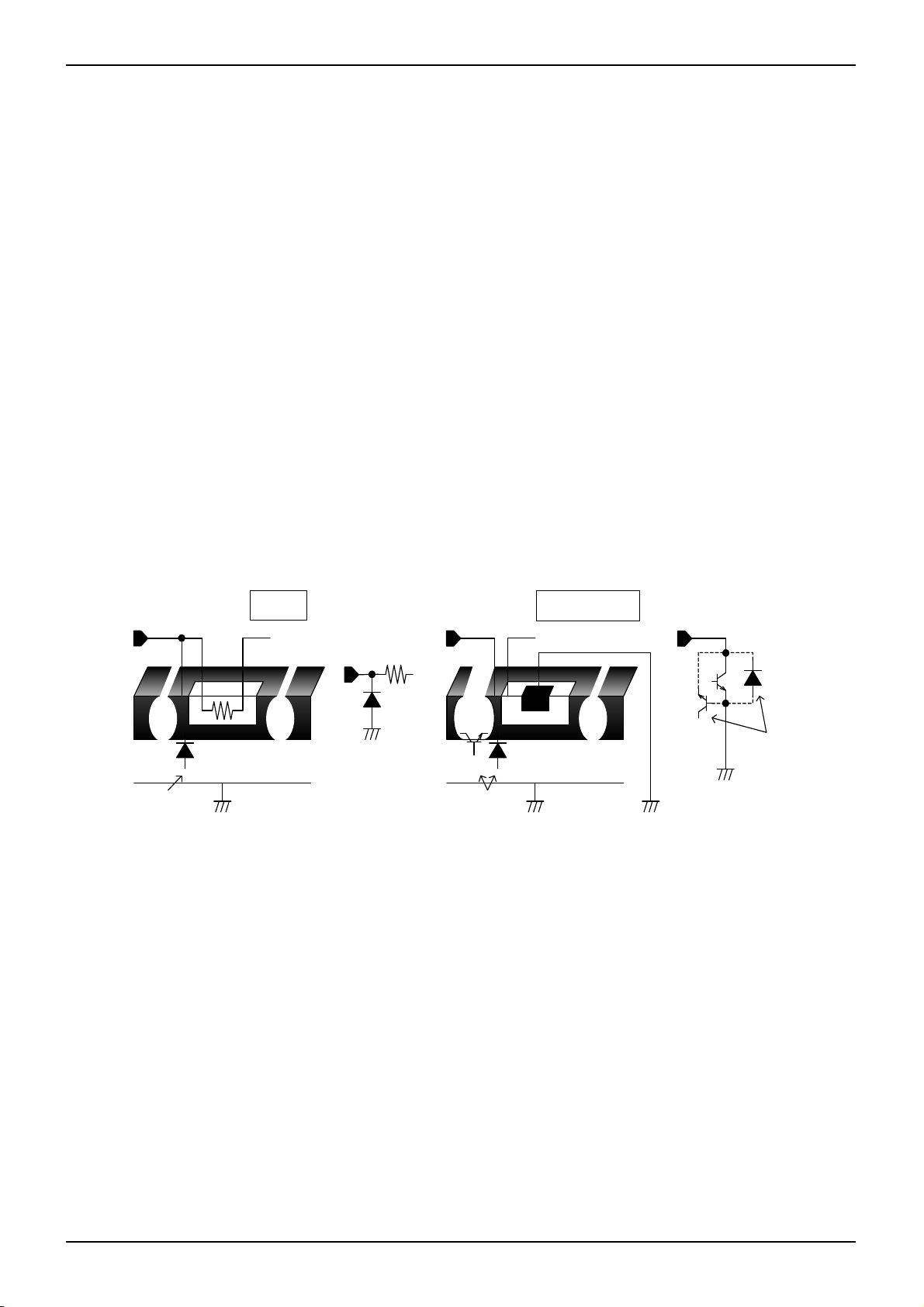
11. IC terminal input
This IC is a monolithic IC, and has P
+
isolation and P substrate for the element separation. Therefore, a parasitic PN
junction is firmed in this P-layer and N-layer of each element. For instance, the resistor or the transistor is connected to
the terminal as shown in the figure below. When the GND voltage potential is greater than the voltage potential at
Terminals A or B, the PN junction operates as a parasitic diode. In addition, the parasitic NPN transistor is formed in said
parasitic diode and the N layer of surrounding elements close to said parasitic diode. These parasitic elements are
formed in the IC because of the voltage relation. The parasitic element operating causes the wrong operation and
destruction. Therefore, please be careful so as not to operate the parasitic elements by impressing to input terminals
lower voltage than GND (P substrate). Please do not apply the voltage to the input terminal when the power-supply
voltage is not impressed. Moreover, please impress each input terminal lower than the power-supply voltage or equal to
the specified range in the guaranteed voltage when the power-supply voltage is impressing.
Terminal-A
+
P
Parasitic
element
Resistor
P
P-Substrate
GND
Transistor(NPN)
GND
Terminal-B
Surrounding
elements
C
B
E
Parasitic
element
GND
Terminal-B
Terminal-A
+
P
Parasitic
element
CB
+
P
Parasitic
element
E
P
P-Substrate
GND
+
P
Simplified structure of IC
12. Earth wiring pattern
Use separate ground lines for control signals and high current power driver outputs. Because these high current outputs
that flows to the wire impedance changes the GND voltage for control signal. Therefore, each ground terminal of IC must
be connected at the one point on the set circuit board. As for GND of external parts, it is similar to the above-mentioned.
www.rohm.com
© 2010 ROHM Co., Ltd. All rights reserved.
21/22
2011.08 - Rev.C
BD8112EFV-M
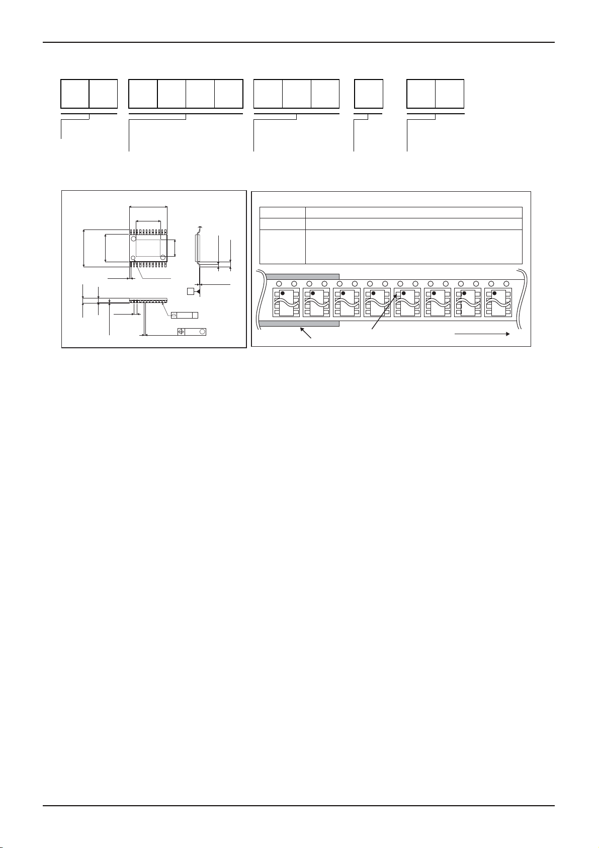
●Ordering part number
Technical Note
B D 8 1
1 2
Part No. Part No. Package
HTSSOP-B24
7.8±0.1
(MAX 8.15 include BURR)
(5.0)
24 13
+
6°
4°
−
4°
+0.05
-
0.04
0.08
(3.4)
S
S
0.08
0.53±0.15
+0.05
0.17
-
M
(Unit : mm)
1.0±0.2
0.03
7.6±0.2
5.6±0.1
112
0.325
1PIN MARK
1.0MAX
0.85±0.05
0.08±0.05
0.65
0.24
E F V - M E 2
Packaging and forming specification
EFV: HTSSOP-B24
<Tape and Reel information>
Embossed carrier tape (with dry pack)Tape
Quantity
Direction
of feed
2000pcs
E2
The direction is the 1pin of product is at the upper left when you hold
()
reel on the left hand and you pull out the tape on the right hand
Reel
1pin
Order quantity needs to be multiple of the minimum quantity.
∗
E2: Embossed tape and reel
Direction of feed
www.rohm.com
© 2010 ROHM Co., Ltd. All rights reserved.
22/22
2011.08 - Rev.C

Notes
No copying or reproduction of this document, in par t or in whole, is permitted without the
consent of ROHM Co.,Ltd.
The content specied herein is subject to change for improvement without notice.
The content specied herein is for the purpose of introducing ROHM's products (hereinafter
"Products"). If you wish to use any such Product, please be sure to refer to the specications,
which can be obtained from ROHM upon request.
Examples of application circuits, circuit constants and any other information contained herein
illustrate the standard usage and operations of the Products. The peripheral conditions must
be taken into account when designing circuits for mass production.
Great care was taken in ensuring the accuracy of the information specied in this document.
However, should you incur any damage arising from any inaccuracy or misprint of such
information, ROHM shall bear no responsibility for such damage.
The technical information specied herein is intended only to show the typical functions of and
examples of application circuits for the Products. ROHM does not grant you, explicitly or
implicitly, any license to use or exercise intellectual property or other rights held by ROHM and
other parties. ROHM shall bear no responsibility whatsoever for any dispute arising from the
use of such technical information.
The Products specied in this document are intended to be used with general-use electronic
equipment or devices (such as audio visual equipment, ofce-automation equipment, communication devices, electronic appliances and amusement devices).
The Products specied in this document are not designed to be radiation tolerant.
While ROHM always makes effor ts to enhance the quality and reliability of its Products, a
Product may fail or malfunction for a variety of reasons.
Please be sure to implement in your equipment using the Products safety measures to guard
against the possibility of physical injury, re or any other damage caused in the event of the
failure of any Product, such as derating, redundancy, re control and fail-safe designs. ROHM
shall bear no responsibility whatsoever for your use of any Product outside of the prescribed
scope or not in accordance with the instruction manual.
The Products are not designed or manufactured to be used with any equipment, device or
system which requires an extremely high level of reliability the failure or malfunction of which
may result in a direct threat to human life or create a risk of human injury (such as a medical
instrument, transportation equipment, aerospace machinery, nuclear-reactor controller, fuelcontroller or other safety device). ROHM shall bear no responsibility in any way for use of any
of the Products for the above special purposes. If a Product is intended to be used for any
such special purpose, please contact a ROHM sales representative before purchasing.
If you intend to export or ship overseas any Product or technology specied herein that may
be controlled under the Foreign Exchange and the Foreign Trade Law, you will be required to
obtain a license or permit under the Law.
Notice
www.rohm.com
© 2011 ROHM Co., Ltd. All rights reserved.
Thank you for your accessing to ROHM product informations.
More detail product informations and catalogs are available, please contact us.
ROHM Customer Support System
http://www.rohm.com/contact/
R1120
A
 Loading...