

A
Standard LDO Regulators
Standard Fixed Output
LDO Regulators
BD80C0AFPS,BD90C0AFPS
●Description
The BD80C0AFPS, BD90C0AFPS is low-saturation regulator. This IC has a built-in over-current protection circuit that
prevents the destruction of the IC due to output short circuits and a thermal shutdown circuit that protects the IC from thermal
damage due to overloading.
●Features
1) Output Current: 1A
2) Output Voltage: 8.0V / 9.0V
3) High Output Voltage Precision: ±1%
4) Low saturation with PDMOS output
5) Built-in over-current protection circuit that prevents the destruction of the IC due to output short circuits
6) Built-in thermal shutdown circuit for protecting the IC from thermal damage due to overloading
7) Low ESR Capacitor
8) TO252S-3 packaging
●Applications
Audiovisual equipments, FPDs, televisions, personal computers or any other consumer device
●Absolute maximum ratings (Ta=25℃)
Parameter Symbol Ratings Unit
Supply Voltage
Power Dissipation
Operating Temperature Range Topr -40 ~ +105 ℃
Storage Temperature Range Tstg -55 ~ +150 ℃
Maximum Junction Temperature Tjmax +150 ℃
*1 Not to exceed Pd.
*2 TO252S-3:Reduced by 9.6mW / °C over Ta = 25°C, when mounted on glass epoxy board: 70mm×70mm×1.6mm.
NOTE: This product is not designed for protection against radioactive rays.
●Operating conditions (Ta=25℃)
■BD80C0AFPS
*1
VCC -0.3 ~ +35.0 V
*2
Pd 1.2 W
No.10021EAT02
Parameter Symbol Min. Max. Unit
Supply Voltage VCC 9.0 25.0 V
Output Current Io 0 1.0 A
■BD90C0AFPS
Parameter Symbol Min. Max. Unit
Supply Voltage Vcc 10.0 25.0 V
Output Current Io 0 1.0 A
www.rohm.com
1/12
© 2010 ROHM Co., Ltd. All rights reserved.
2010.11 - Rev.

A
BD80C0AFPS,BD90C0AFPS
●Electrical characteristics
■BD80C0AFPS
(Unless otherwise specified, Ta=25℃, Vcc=13V, Io=0mA)
Parameter Symbol Min Typ Max Unit Conditions
Bias Current Ib - 0.6 1.0 mA
Output Voltage Vo 7.92 8.00 8.08 V Io=500mA
Dropout Voltage ΔVd - 0.3 0.5 V VCC=Vo×0.95, Io=500mA
Technical Note
Ripple Rejection R.R. 40 50 - dB
Line Regulation Reg.I - 20 60 mV VCC=9→25V
Load Regulation Reg.L - Vo×0.010 Vo×0.015 V Io=5mA→1A
Temperature Coefficient of
Output Voltage
*1 ein: Input Voltage Ripple
■BD90C0AFPS
(Unless otherwise specified, Ta=25℃, Vcc=14V, Io=0mA)
Parameter Symbol Min Typ Max Unit Conditions
Bias Current Ib - 0.6 1.0 mA
Output Voltage Vo 8.91 9.00 9.09 V Io=500mA
Dropout Voltage ΔVd - 0.3 0.5 V VCC=Vo×0.95, Io=500mA
Ripple Rejection R.R. 40 50 - dB
Line Regulation Reg.I - 20 60 mV VCC=10→25V
Tcvo.1 - +0.04 - %/℃ Io=5mA,Tj=-40 ~ -20℃
Tcvo.2 - ±0.005 - %/℃ Io=5mA,Tj=-20 ~ +105℃
f=120Hz,ein*1=1Vrms,
Io=100mA
f=120Hz,ein*1=1Vrms,
Io=100mA
Load Regulation Reg.L - Vo×0.010 Vo×0.015 V Io=5mA→1A
Temperature Coefficient of
Output Voltage
*1 ein: Input Voltage Ripple
Tcvo.1 - +0.04 - %/℃ Io=5mA,Tj=-40 ~ -20℃
Tcvo.2 - ±0.005 - %/℃ Io=5mA,Tj=-20 ~ +105℃
www.rohm.com
2/12
© 2010 ROHM Co., Ltd. All rights reserved.
2010.11 - Rev.
A
BD80C0AFPS,BD90C0AFPS
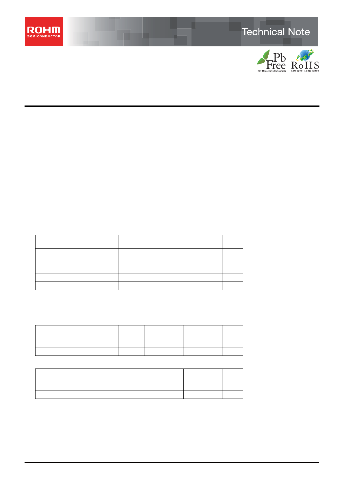
●Electrical characteristic curves (Reference data)
BD80C0AFPS(Unless otherwise specified, Ta=25℃, Vcc=13V, Io=0mA)
1.0
0.8
0.6
0.4
0.2
CIRCUIT CURRENT: Ib[mA]
0.0
0246 81012141618202224
SUPPLY VOLTAGE: Vcc [V]
Fig.1 Circuit Current
10
9
8
7
6
5
4
3
2
OUTPU T VOLTAGE: Vo [V]
1
0
0 2 4 6 8 10 12 14 16 18 20 22 24
SUPPLY VOLT AGE: Vcc [V]
Fig.2 Line Regulation
(Io=0mA)
10
9
8
7
6
5
4
3
2
OUT PUT VO LTAGE : Vo [V]
1
0
0 400 800 1200 1600 2000
OUTPUT CURRENT: I
Fig.4 Load Regulation
10
9
8
7
6
5
4
3
OUTPU T VOLTAGE: Vo [V]
2
1
0
-40 -20 0 20 40 60 80 100
AMBIEN T T EMPER ATU RE: T a
Fig.7 Output Voltage
Temperature Characteristics
O
[mA]
[℃]
600
500
Vd [mV]
Δ
400
300
200
100
DROPOUT VOLTAGE :
0
0 200 400 600 800 1000
OUTPUT CURRENT: IO [mA]
Fig.5 Dropout Voltage
(Vcc=Vo×0.95V)
(lo=0mA→1000mA)
1.0
0.8
0.6
0.4
CIRCUIT CURRENT: Ib[mA]
0.2
0.0
0 200 400 600 800 1000
OUTPUT CURRENT: Io [ mA]
Fig.8 Circuit Current
(lo=0mA→1000 mA)
Technical Note
10
9
8
7
6
5
4
3
2
OUT PUT VO LTAGE: Vo [V]
1
0
024681012141618202224
SUPPLY VOLTAGE: Vcc [V]
Fig.3 Line Regulation
(Io=500mA)
80
70
60
50
40
30
20
RIPPLE REJECTION : R.R. [dB]
10
0
10 100 1000 10000 100000 1000000
10
9
8
7
6
5
4
3
OUTPU T VOLTAGE: Vo [V]
2
1
0
130 140 150 160 170 180 190
FREQU ENCY: f [H z]
Fig.6 Ripple Rejection
(Io =100mA)
AMBIEN T T EMPER ATU RE: T a [℃]
Fig.9 Thermal Shutdown
Circuit Characteristics
www.rohm.com
3/12
© 2010 ROHM Co., Ltd. All rights reserved.
2010.11 - Rev.
A
BD80C0AFPS,BD90C0AFPS
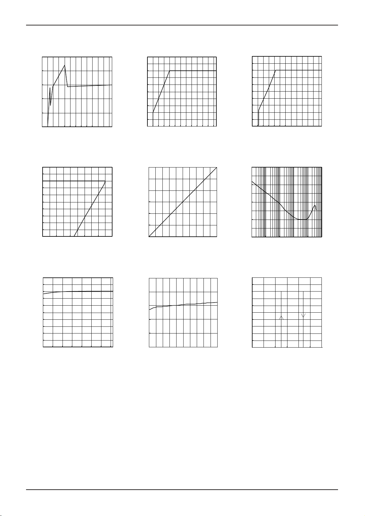
●Electrical characteristic curves (Reference data)
BD90C0AFPS(Unless otherwise specified, Ta=25℃, Vcc=14V, Io=0mA)
1.0
0.8
0.6
0.4
0.2
CIRCUIT CURRENT: Ib[mA]
0.0
024681012141618202224
SUPPLY VOLTAGE: Vcc [V]
10
9
8
7
6
5
4
3
2
OUTPU T VOLTAGE: Vo [V]
1
0
024681012141618202224
SUPPLY VOLTAGE: Vcc [V]
Fig.10 Circuit Current
Fig.11 Line Regulation
(Io=0mA)
10
9
8
7
6
5
4
3
OUTPU T VOLTAGE: Vo [V]
2
1
0
0 400 800 1200 1600 2000
OUTPUT CURRENT: IO[mA]
Fig.13 Load Regulation
10
9
8
7
6
5
4
3
2
OUTPU T VOLTAGE : Vo [V]
1
0
-40 -20 0 20 40 60 80 100
AMBIEN T TEMPER ATURE: T a[℃]
Fig.16 Output Voltage
Temperature Characteristics
600
500
Vd [mV]
Δ
400
300
200
100
DR OPOUT VOLT AGE:
0
0 200 400 600 800 1000
OUTPUT CURRENT: [mA]
Fig.14 Dropout Voltage
(Vcc=Vo×0.95V)
(lo=0mA→1000mA)
1.0
0.8
0.6
0.4
0.2
CIRCUIT CURRENT: Ib[mA]
0.0
0 200 400 600 800 1000
OUTPUT CURRENT: Io [mA]
Fig.17 Circuit Current
(lo=0mA→1000 mA)
Technical Note
10
9
8
7
6
5
4
3
2
OUTPU T VOLTAGE : Vo [V]
1
0
024681012141618202224
SUPPLY VOLTAGE: Vcc [V]
Fig.12 Line Regulation
(Io=500mA)
80
70
60
50
40
30
20
RIPPLE REJECTION: R.R. [dB]
10
0
10 100 1000 10000 100000 1000000
10
9
8
7
6
5
4
3
2
OUTPU T VOLTAGE : Vo [V]
1
0
130 140 150 160 170 180 190
FREQU ENCY: f [Hz]
Fig.15 Ripple Rejection
(Io=100mA)
AMBIENT TEM PERATU RE: Ta [
Fig.18 Thermal Shutdown
Circuit Characteristics
]
℃
www.rohm.com
4/12
© 2010 ROHM Co., Ltd. All rights reserved.
2010.11 - Rev.

A
BD80C0AFPS,BD90C0AFPS
●BD80C0AFPS, BD90C0AFPS Measurement Circuit for Reference Data
1µF
A
Vcc
GND
Vo
1µF
Vcc
1µF
GND
Vo
1µF
Measurement Circuit of Fig.1 and Fig.10
Measurement Circuit of Fig.2 and Fig.11 Measurement Circuit of Fig .3 and Fig.12
Vcc
1µF
GND
Vo
1µF 1µF
A
A
1µF
Vcc
V
Vo
GND
Measurement Circuit of Fig .4 and Fig.13
Measurement Circuit of Fig.5 and Fig.14 Measurement Circuit of Fig.6 and Fig.15
Vcc
1µF
GND
Vo
1 µ F 1 µ F 1µ F
V
Vcc
1µF
Vo
GND
A
Measurement Circuit of Fig .7 and Fig.16 Measurement Circuit of Fig.8 and Fig.17
Technical Note
Vcc
GND
Vcc
GND
Vo
GND
1µF
Vo
Vo
V
500mA
1µF
100mA
V
Vcc
1Vrms
1µF
1µF
~
1µF
V
Measurement Circuit of Fig.9 and Fig.18
www.rohm.com
5/12
© 2010 ROHM Co., Ltd. All rights reserved.
2010.11 - Rev.

A
BD80C0AFPS,BD90C0AFPS
●BD80C0AFPS, BD90C0AFPS Block diagrams
VREF
OCP
1
Vcc
Pin No.. Pin Name Function
1 Vcc Power Supply Pin
2 N.C. N.C. Pin
3 Vo Output Pin
FIN GND GND
●Package dimensions
●Input / Output Equivalent Circuit Diagrams
Pin
Vcc
Vcc
IC
Circuit
Vo
TSD
Pin
20kΩ
GND
FIN
2
N.C.
Fig.19
Driver
Vcc
48.3kΩ(80)
55kΩ(90)
5kΩ
VREF:
Bandgap Reference
OCP:
Over Current P rotection Circuit
Thermal Shut Down Circuit
TSD:
Driver:
Power Transistor Driver
3
Vo
Technical Note
Vo
www.rohm.com
6/12
© 2010 ROHM Co., Ltd. All rights reserved.
2010.11 - Rev.

A
BD80C0AFPS,BD90C0AFPS
Technical Note
●Thermal Design
5
4
3
2
Power Di ssipati on: Pd (W )
1.20
1
Mounted on a Rohm standard board
Board size : 70mm
Copper foil area :7mm
TO252-3
×70 mm×1.6 mm
θja=104.2(℃/W)
×7mm
5
4.80
③
4
3.50
②
3
1.85
①
2
Power Di ssipati on: Pd (W )
1
Mounted on a Rohm standard board
Board size : 70mm
Copper foil area :7mm
①2-layer board
(back surface copper foil area :15mm×15mm)
②2-layer board
(back surface copper foil area :70mm×70mm)
③4-layer board
(back surface copper foil area :70mm×70mm))
①:θja=67.6℃/W
②:θja=35.7℃/W
③:θja=26.0℃/W
×70 mm×1.6 mm
×7mm
0
0 25 50 75 100 125 150
Ambient T emperat ure: Ta
(℃)
Fig.20 Fig.21(reference data)
0
0 25 50 75 100 125 150
Ambient T emperat ure: Ta
(℃)
When using at temperatures over Ta=25℃, please refer to the heat reducing characteristics shown in Fig.20 and Fig.21.
The IC characteristics are closely related to the temperature at which the IC is used, so it is necessary to operate the IC at
temperatures less than the maximum junction temperature Tjmax.
Fig.20 and Fig.21 shows the acceptable loss and heat reducing characteristics of the TO252S-3 package. Even when the
ambient temperature Ta is a normal temperature (25℃), the chip (junction) temperature Tj may be quite high so please
operate the IC at temperatures less than the acceptable loss Pd.
The calculation method for power consumption Pc(W) is as follows :(Fig.21③)
Pc=(Vcc-Vo)×Io+Vcc×Ib
Acceptable loss Pd≧Pc
Solving this for load current Io in order to operate within the acceptable loss,
Io≦
Pd-Vcc×Ib
Vcc-Vo
Vcc:
Vo:
Io:
Ib:
Ishort:
Input voltage
Output voltage
Load current
Circuit current
Short current
(Please refer to Fig.8,Fig.17 for Ib.)
It is then possible to find the maximum load current Io
Max with respect to the applied voltage Vcc at the time of thermal
design.
Calculation Example for BD80C0AFPS)
When Ta=85℃, Vcc=13V, Vo=8V
Io≦
2.496-13×Ib
5
Fig.21③ :θja=26.0℃/W → -38.4mW/℃
25℃=4.80W → 85℃=2.496W
Io≦497.6mA (Ib: 0.6 mA)
Please refer to the above information and keep thermal designs within the scope of acceptable loss for all operating
temperature ranges. The power consumption Pc of the IC when there is a short circuit (short between Vo and GND) is :
Pc=Vcc×(Ib + Ishort) (Please refer to Fig.4,Fig.13 for Ishort.)
www.rohm.com
7/12
© 2010 ROHM Co., Ltd. All rights reserved.
2010.11 - Rev.

A
BD80C0AFPS,BD90C0AFPS
●Notes for use
1. Absolute maximum ratings
Use of the IC in excess of absolute maximum ratings (such as the input voltage or operating temperature range) may
result in damage to the IC. Assumptions should not be made regarding the state of the IC (e.g., short mode or open mode)
when such damage is suffered. If operational values are expected to exceed the maximum ratings for the device, consider
adding protective circuitry (such as fuses) to eliminate the risk of damaging the IC.
2. Electrical characteristics described in these specifications may vary, depending on temperature, supply voltage external
circuits and other conditions. Therefore, be sure to check all relevant factors, including transient characteristics.
3. GND potential
The potential of the GND pin must be the minimum potential in the system in all operating conditions. Ensure that no pins
are at a voltage below the GND at any time, regardless of transient characteristics.
4. Ground wiring pattern
When using both small-signal and large-current GND traces, the two ground traces should be routed separately but
connected to a single ground potential within the application in order to avoid variations in the small-signal ground caused
by large currents. Also ensure that the GND traces of external components do not cause variations on GND voltage. The
power supply and ground lines must be as short and thick as possible to reduce line impedance.
5. Inter-pin shorts and mounting errors
Use caution when orienting and positioning the IC for mounting on printed circuit boards. Improper mounting may result in
damage to the IC. Shorts between output pins or between output pins and the power supply or GND pins (caused by poor
soldering or foreign objects) may result in damage to the IC.
6. Operation in strong electromagnetic fields
Using this product in strong electromagnetic fields may cause IC malfunction. Caution should be exercised in applications
where strong electromagnetic fields may be present.
7. Testing on application boards
When testing the IC on an application board, connecting a capacitor directly to a low-impedance pin may subject the IC to
stress. Always discharge capacitors completely after each process or step. The IC’s power supply should always be
turned off completely before connecting or removing it from a jig or fixture during the evaluation process. To prevent
damage from static discharge, ground the IC during assembly and use similar precautions during transport and storage.
8. Thermal consideration
Use a thermal design that allows for a sufficient margin in light of the Pd in actual operating conditions.
Consider Pc that does not exceed Pd in actual operating conditions. (Pd≧Pc)
Tjmax: Maximum junction temperature=150℃, Ta: Peripheral temperature[℃] ,
θja: Thermal resistance of package-ambience[℃/W], Pd: Package Power dissipation [W]
Pc: Power dissipation [W], Vcc: Input Voltage, Vo: Output Voltage, Io: Load, Ib: Bias Current
9. Vcc pin
Insert a capacitor(capacitor≧1µF ~ ) between the Vcc and GND pins. The appropriate capacitance value varies by
application. Be sure to allow a sufficient margin for input voltage levels.
Electric capacitance
IC
Ceramic capacitors,Low ESR capacitors
Technical Note
www.rohm.com
8/12
© 2010 ROHM Co., Ltd. All rights reserved.
2010.11 - Rev.

A
BD80C0AFPS,BD90C0AFPS
Technical Note
10. Output pins
It is necessary to place capacitors between each output pin and GND to prevent oscillation on the output.
Usable capacitance values range from 1µF to 1000µF. Ceramic capacitors can be used as long as their ESR value is low
enough to prevent oscillation (0.001Ω to 20Ω). Abrupt fluctuations in input voltage and load conditions may affect the
output voltage. Output capacitance values should be determined only through sufficient testing of the actual application.
Vcc=9V~25V(BD80C0AFPS)
~25V(BD90C0AFPS)
Vcc=10V
℃~+105℃
Ta= - 40
~100µF Cout=1µF~100µF
Cin=1µF
Cout_ESR(Ω)
100
10
1
0.1
0.01
0.001
Unstable operating region
Stable operating region
0 200 400 600 800 1000
Io(mA)
Cout_ESR vs Io(reference data)
~25V(BD80C0AFPS)
Vcc=9V
~25V(BD90C0AFPS)
Vcc=10V
℃~+105℃
Ta= - 40
~100µF Cout=1µF~100µF
Cin=1µF
~1A
Io=0A
100
10
Cin(μF)
1
1
Stable operating region
10
Cout(μF)
100
Cin vs Cout(reference data)
Vcc
Cin
(1µF~ )
Vcc
Vo
GND
Cout(1µF~ )
ESR
(0.001Ω~ )
Io(ROUT)
※Operation Notes10 Measurement circuit
11. For a steep change of the Vcc voltage
Because MOS for output Transistor is used when an input voltage change is very steep, it may evoke large current.
When selecting the value of external circuit constants, please make sure that the operation on the actual application takes
these conditions into account.
12. For an infinitesimal fluctuations of output voltage.
At the use of the application that infinitesimal fluctuations of output voltage caused by some factors (e.g. disturbance noise,
input voltage fluctuations, load fluctuations, etc.), please take enough measures to avoid some influence (e.g. insert the
filter, etc.).
13. Over current protection circuit (OCP)
The IC incorporates an integrated over-current protection circuit that operates in accordance with the rated output capacity.
This circuit serves to protect the IC from damage when the load becomes shorted. It is also designed to limit output current
(without latching) in the event of a large and instantaneous current flow from a large capacitor or other component. These
protection circuits are effective in preventing damage due to sudden and unexpected accidents. However, the IC should
not be used in applications characterized by the continuous or transitive operation of the protection circuits.
14. Thermal shutdown circuit (TSD)
The IC incorporates a built-in thermal shutdown circuit, which is designed to turn the IC off completely in the event of
thermal overload. It is not designed to protect the IC from damage or guarantee its operation. ICs should not be used after
this function has activated, or in applications where the operation of this circuit is assumed.
www.rohm.com
9/12
© 2010 ROHM Co., Ltd. All rights reserved.
2010.11 - Rev.

A
BD80C0AFPS,BD90C0AFPS
Technical Note
15. Applications or inspection processes where the potential of the Vcc pin or other pins may be reversed from their normal
state may cause damage to the IC's internal circuitry or elements. Use an output pin capacitance of 1000µF or lower in
case Vcc is shorted with the GND pin while the external capacitor is charged. Insert a diode in series with Vcc to prevent
reverse current flow, or insert bypass diodes between Vcc and each pin.
16. Positive voltage surges on V
A power zener diode should be inserted between V
pin.
the V
CC
CC
pin
and GND for protection against voltage surges of more than 35V on
CC
Vcc
GND
17. Negative voltage surges on V
A schottky barrier diode should be inserted between V
pin.
V
CC
CC
pin
and GND for protection against voltages lower than GND on the
CC
Vcc
GND
18. Output protection diode
Loads with large inductance components may cause reverse current flow during startup or shutdown. In such cases, a
protection diode should be inserted on the output to protect the IC.
www.rohm.com
10/12
© 2010 ROHM Co., Ltd. All rights reserved.
2010.11 - Rev.

A
BD80C0AFPS,BD90C0AFPS
Technical Note
19. Regarding input pins of the IC
This monolithic IC contains P+ isolation and P substrate layers between adjacent elements in order to keep them isolated.
PN junctions are formed at the intersection of these P layers with the N layers of other elements, creating parasitic diodes
and/or transistors. For example (refer to the figure below):
○When GND > Pin A and GND > Pin B, the PN junction operates as a parasitic diode
○When GND > Pin B, the PN junction operates as a parasitic transistor
Parasitic diodes occur inevitably in the structure of the IC, and the operation of these parasitic diodes can result in mutual
interference among circuits, operational faults, or physical damage. Accordingly, conditions that cause these diodes to
operate, such as applying a voltage lower than the GND voltage to an input pin (and thus to the P substrate) should be
avoided.
(Pin A)
Resistor
(Pin B)
P+
N
P
P
N
GND
P+
N
Parasitic elements
Parasitic elements
or transistors
N
Transistor (NPN)
C
P+
B
E
N
P
N
P substrate
GND
P+
(Pin B)
C
B
E
GND
N
(Pin A)
Parasitic elements
or transistors
Parasitic elements
Example of Simple Monolithic IC Architecture
www.rohm.com
11/ 1 2
© 2010 ROHM Co., Ltd. All rights reserved.
2010.11 - Rev.

A
BD80C0AFPS,BD90C0AFPS
●Ordering part number
B D 8 0 C 0 A F P S - E 2
ROHM
model Name
Output Voltage
80:8V Output
90:9V Output
Current capacity
C0A:1A
Package
FPS:TO252S-3
Packaging specification
E2: Embossed tape and reel
Technical Note
www.rohm.com
12/12
© 2010 ROHM Co., Ltd. All rights reserved.
2010.11 - Rev.

Notes
No copying or reproduction of this document, in part or in whole, is permitted without the
consent of ROHM Co.,Ltd.
The content specied herein is subject to change for improvement without notice.
The content specied herein is for the purpose of introducing ROHM's products (hereinafter
"Products"). If you wish to use any such Product, please be sure to refer to the specications,
which can be obtained from ROHM upon request.
Examples of application circuits, circuit constants and any other information contained herein
illustrate the standard usage and operations of the Products. The peripheral conditions must
be taken into account when designing circuits for mass production.
Great care was taken in ensuring the accuracy of the information specied in this document.
However, should you incur any damage arising from any inaccuracy or misprint of such
information, ROHM shall bear no responsibility for such damage.
The technical information specied herein is intended only to show the typical functions of and
examples of application circuits for the Products. ROHM does not grant you, explicitly or
implicitly, any license to use or exercise intellectual property or other rights held by ROHM and
other parties. ROHM shall bear no responsibility whatsoever for any dispute arising from the
use of such technical information.
Notice
The Products specied in this document are intended to be used with general-use electronic
equipment or devices (such as audio visual equipment, of ce-automation equipment, communication devices, electronic appliances and amusement devices).
The Products specied in this document are not designed to be radiation tolerant.
While ROHM always makes effor ts to enhance the quality and reliability of its Products, a
Product may fail or malfunction for a variety of reasons.
Please be sure to implement in your equipment using the Products safety measures to guard
against the possibility of physical injur y, re or any other damage caused in the event of the
failure of any Product, such as derating, redundancy, re control and fail-safe designs. ROHM
shall bear no responsibility whatsoever for your use of any Product outside of the prescribed
scope or not in accordance with the instruction manual.
The Products are not designed or manufactured to be used with any equipment, device or
system which requires an extremely high level of reliability the failure or malfunction of which
may result in a direct threat to human life or create a risk of human injury (such as a medical
instrument, transportation equipment, aerospace machinery, nuclear-reactor controller, fuelcontroller or other safety device). ROHM shall bear no responsibility in any way for use of any
of the Products for the above special purposes. If a Product is intended to be used for any
such special purpose, please contact a ROHM sales representative before purchasing.
If you intend to export or ship overseas any Product or technology specied herein that may
be controlled under the Foreign Exchange and the Foreign Trade Law, you will be required to
obtain a license or permit under the Law.
Thank you for your accessing to ROHM product informations.
More detail product informations and catalogs are available, please contact us.
ROHM Customer Support System
www.rohm.com
© 2010 ROHM Co., Ltd. All rights reserved.
http://www.rohm.com/contact/
R1010
A
 Loading...