

A
Class-AB Speaker Amplifiers
1.9W+1.9W
Stereo Speaker Amplifier
BD7836EFV
●Description
BD7836EFV is a Class-AB stereo speaker amplifier, developed for note-book PC, desktop PC, portable devices and others.
Class-AB amplifier has no EMI noise. Power package HTSSOP-B20 can realize high output power.
Low circuit current at active mode reduce consumption of battery. Shutdown current is 0.1µA typically, and pop noise level
when shutdown turns on and off is very small. This device is suitable for the application that often changes mode between
“shutdown state” and “active state”.
●Features
1) High power 1.9W typ. (VDD=5V, R
High power 1.2W typ. (VDD=5V, R
2) Gain selectable by the external control (6,10,15.6,21.6dB)
3) Pop noise suppression circuitry
4) Shutdown function (also Mute function) [I
5) Protection circuitry (Thermal shutdown, Under voltage lockout)
6) Power Package with thermal pad HTSSOP-B20
●Applications
Note-book PC, Desktop PC, etc.
●Absolute maximum ratings (Ta=+25℃)
Parameter Symbol Ratings Unit
Power Supply Voltage VDDmax 7.0 V
Power Dissipation Pd
L=4Ω, THD+N=1%, stereo input)
L=8Ω, THD+N=1%, stereo input)
=0.1µA(typ.)]
sd
1
3.2 *2 W
*1
W
No.10077EAT07
Storage Temperature Tstg -55 ~ +150 ℃
Input Terminal Input Voltage Range *3 Vin -0.3~VDD+0.3 V
Control Terminal Input Voltage Range *4 Vctl -0.3~VDD+0.3 V
*1 70mm×70mm×1.6mm FR4 1-layer glass epoxy board(Copper on top layer 0%)
Derating in done at 8mW/℃ for operating above Ta=25℃. There are thermal via on the board.
*2 70mm×70mm×1.6mm FR4 4-layer glass epoxy board (Copper on bottom 2 and 3 layer 100%)
Derating in done at 25.6mW/℃ for operating above Ta=25℃. There are thermal via on the board.
*3 Input Terminal (LIN+, LIN-, RIN+, RIN-)
*4 Control Terminal (
●Operating conditions
Power Supply Voltage
Temperature
* These products aren’t designed for protection against radioactive rays.
SHUTDOWN
Parameter
, GAIN0, GAIN1)
Symbol Range Unit
VDD +4.5 ~ +5.5 V
Topr -40 ~ +85 ℃
www.rohm.com
1/16
© 2010 ROHM Co., Ltd. All rights reserved.
2010.07 - Rev.
BD7836EFV
A
●Electric characteristic (Unless otherwise specified, Ta=+25℃, VDD=+5.0V, RL=8Ω, AC stereo input)
Technical Note
Parameter Symbol
Min. Typ. Max.
Circuit current (Active) Icc ― 5 10 mA
Circuit current (Shutdown) Isd ― 0.1 2.0 µA
Limits
Unit Condition
IC active, No load
SHUTDOWN
=Hi
IC Shutdown
SHUTDOWN
=Lo
<Speaker amplifier>
Output power 1 PO1 0.7 1.2 ― W RL=8Ω, BTL, f=1kHz, THD+N=1% *1
Output power 2 PO2 ― 1.9 ― W RL=4Ω, BTL, f=1kHz, THD+N=1% *1
5.5 6.0 6.5 dB BTL, GAIN0=GAIN1=L
Gain GV
9.5 10 10.5 dB BTL, GAIN0=L, GAIN1=H
14.6 15.6 16.5 dB BTL, GAIN0=H, GAIN1=L
20.6 21.6 22.6 dB BTL, GAIN0=GAIN1=H
63 90 117 kΩ GAIN0=GAIN1=L
Input resistance R
IN
49 70 91 kΩ GAIN0=L, GAIN1=H
31 45 59 kΩ GAIN0=H, GAIN1=L
17 25 33 kΩ GAIN0=GAIN1=H
Supply ripple rejection ratio PSRR 62 68 ― dB
Vripple=0.2Vp-p,C
f=1kHz, BTL
=0.47µF
BYP
Output noise Vnoise ― 16 80 µVrms BTL, f=1kHz, 20-20kHz
S/N SN ― 105 ― dB BTL, Po=1W, BTL, f=1kHz, 20-20kHz
Output DC offset voltage ⊿Vo ― 0 ±25 mV
<Control terminal (
Control terminal
Input voltage
*1: B.W.=400~30kHz, BTL:The voltage between 4pin and 8pin, 14pin and 18pin.
SHUTDOWN
,GAIN0,GAIN1)>
Hi level VIH 2.0 ― VDD V
Lo level VIL 0 ― 0.8 V
●Control terminal’s settings
SHUTDOWN
IC condition
Hi Active
Lo Shutdown
GAIN0 GAIN1 Gain Input resistance
Lo Lo 6dB 90kΩ (TYP.)
Lo Hi 10dB 70kΩ (TYP.)
Hi Lo 15.6dB 45kΩ (TYP.)
Hi Hi 21.6dB 25kΩ (TYP.)
www.rohm.com
2/16
© 2010 ROHM Co., Ltd. All rights reserved.
2010.07 - Rev.
BD7836EFV
A
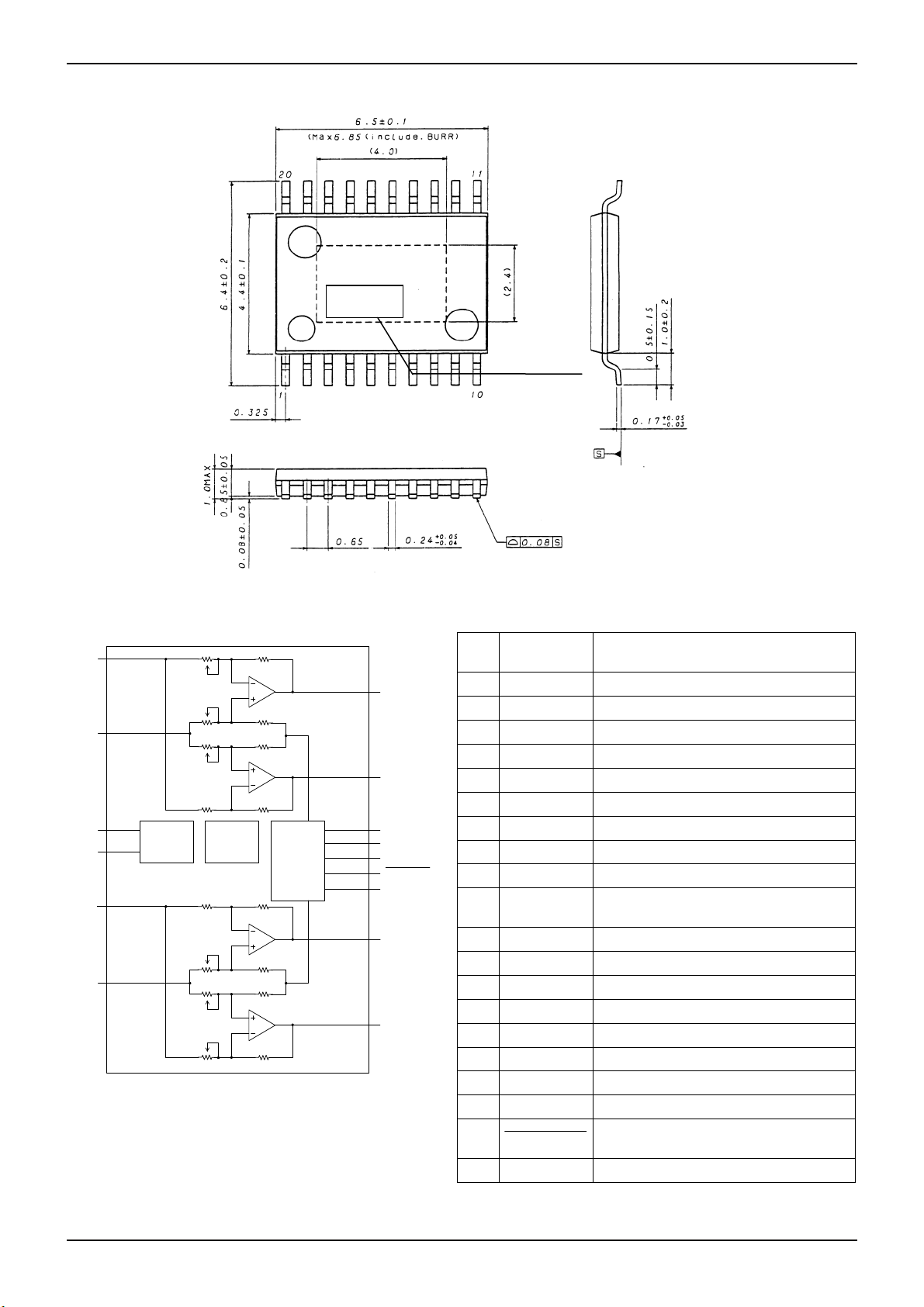
●Package outlines
BD7836
Lot No.
Fig.1 HTSSOP-B20
●Block diagram ●Pin assignment table
Pin
RIN-
ROUT+
Terminal name Function
No.
1 GND Ground
2 GAIN0 Bit 0 of gain select
RIN+
3 GAIN1 Bit 1 of gain select
4 LOUT+ Left channel positive output
ROUT-
5 LIN- Left channel negative differential input
6 PVDD Supply voltage terminal
GAIN0
GAIN1
LIN-
Gain
Control
Depop
Circuitry
Power
Management
PVDD
VDD
BYPASS
SHUTDOWN
GND
LOUT+
7 RIN+ Right channel negative differential input
8 LOUT- Left channel negative output
9 LIN+ Left channel positive differential input
10 BYPASS
11 GND Ground
12 NC No connection
LIN+
LOUT-
13 GND Ground
14 ROUT- Right channel negative output
15 PVDD Supply voltage terminal
16 VDD Supply voltage terminal
17 RIN- Right channel negative differential input
Fig.2
18 ROUT+ Right channel positive output
SHUTDOWN
19
20 GND Ground
Technical Note
(unit : mm)
Tap to voltage divider for internal
midsupply bias generator
Places IC in shutdown mode when
held low
www.rohm.com
3/16
© 2010 ROHM Co., Ltd. All rights reserved.
2010.07 - Rev.
BD7836EFV
A
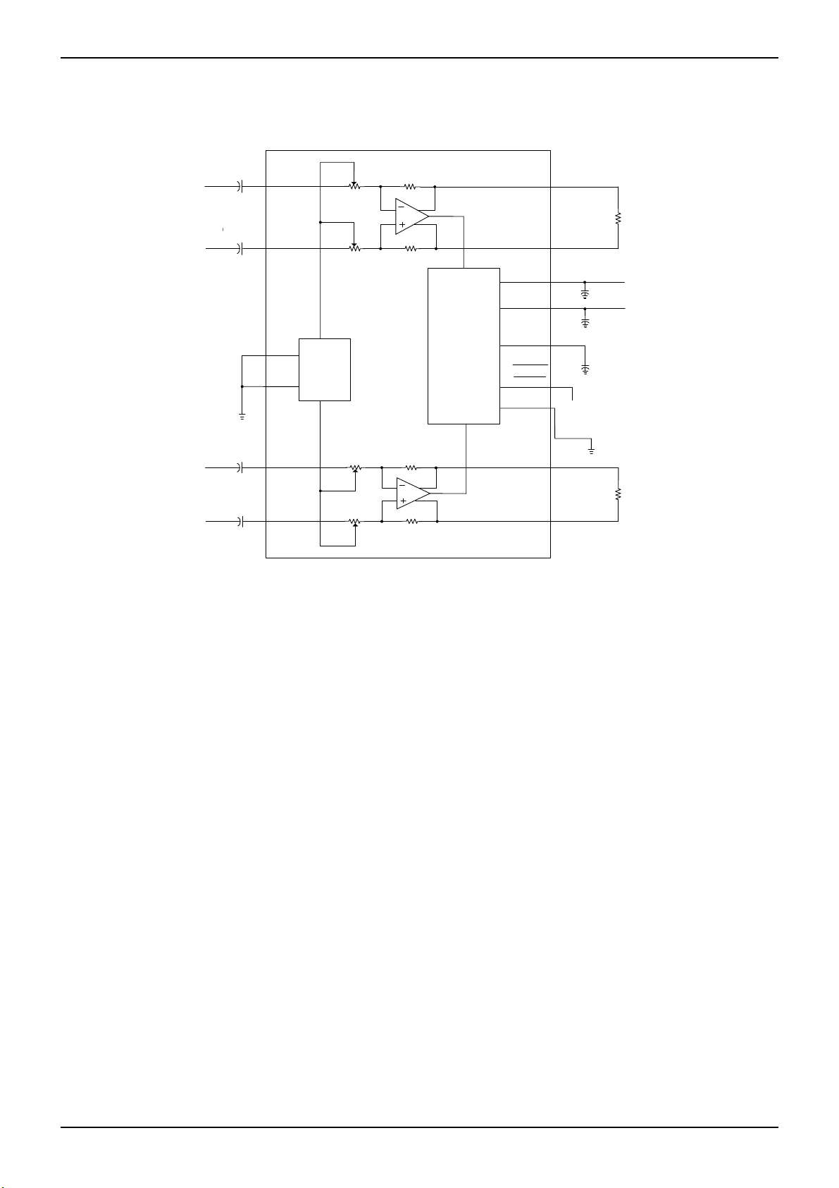
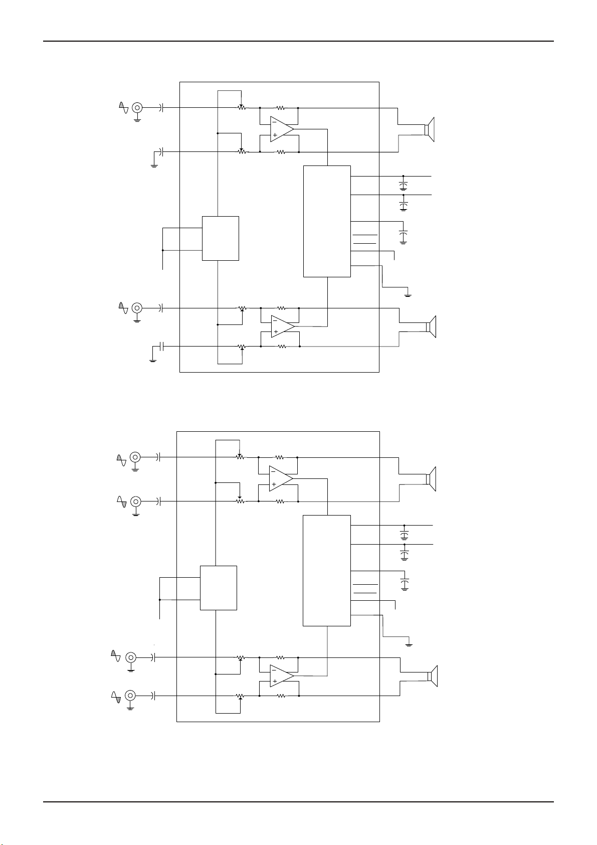
●Measurement circuit diagram
Right
Line
Input
Signal
C
0.47µF
C
RIN
0.47µF
Left
Line
Input
Signal
C
0.47µF
C
LIN
0.47µF
Technical Note
-
RIN
18
17
RIN-
+
+
7
RIN+
2
GAIN0
GAIN1
3
-
LIN
5
LIN-
+
LIN+
98
Gain
Control
-
Power
Management
+
-
Fig.3
ROUT+
ROUT-
PVDD
VDD
BYPASS
SHUT-
DOWN
GND
LOUT+
LOUT-
14
6.15
C
16
C
10
C
19
To
System Control
4
SR
0.1µF
SR
0.1µF
BYP
0.47µF
1,11,
13,20
RL
RL
V
DD
V
DD
www.rohm.com
4/16
© 2010 ROHM Co., Ltd. All rights reserved.
2010.07 - Rev.
BD7836EFV
A
Technical Note
●Application circuit example
Right
Line
Input
Signal
C
RIN
0.47µF
Left
Line
Input
Signal
0.47µF
Right
Line
Input
Signal
0.47µF
0.47µF
Left
Line
Input
Signal
C
0.47µF
C
0.47µF
C
-
RIN
0.47µF
17
RIN-
+
+
7
RIN+
GAIN0
2
GAIN1
3
-
C
LIN
0.47µF
LIN-
5
C
LIN+
LIN+
98
Gain
Control
-
+
-
Power
Management
ROUT+
ROUT-
PVDD
VDD
BYPASS
SHUT-
DOWN
GND
LOUT+
LOUT-
18
14
6.15
16
10
19
To
4
V
C
SR
0.1µF
V
C
SR
0.1µF
C
BYP
0.47µF
System Control
1,11,
13,20
DD
DD
Fig.4 Single Ended inputs
C
RIN-
18
17
RIN-
+
C
RIN+
7
RIN+
GAIN0
2
GAIN1
3
LIN-
LIN-
5
LIN+
LIN+
98
Gain
Control
-
+
-
Power
Management
ROUT+
ROUT-
PVDD
VDD
BYPASS
SHUT-
DOWN
GND
LOUT+
LOUT-
14
6.15
16
10
19
To
4
V
C
SR
0.1µF
V
C
SR
0.1µF
C
BYP
0.47µF
System Control
1,11,
13,20
DD
DD
Fig.5 Differential inputs
www.rohm.com
5/16
© 2010 ROHM Co., Ltd. All rights reserved.
2010.07 - Rev.
BD7836EFV
A
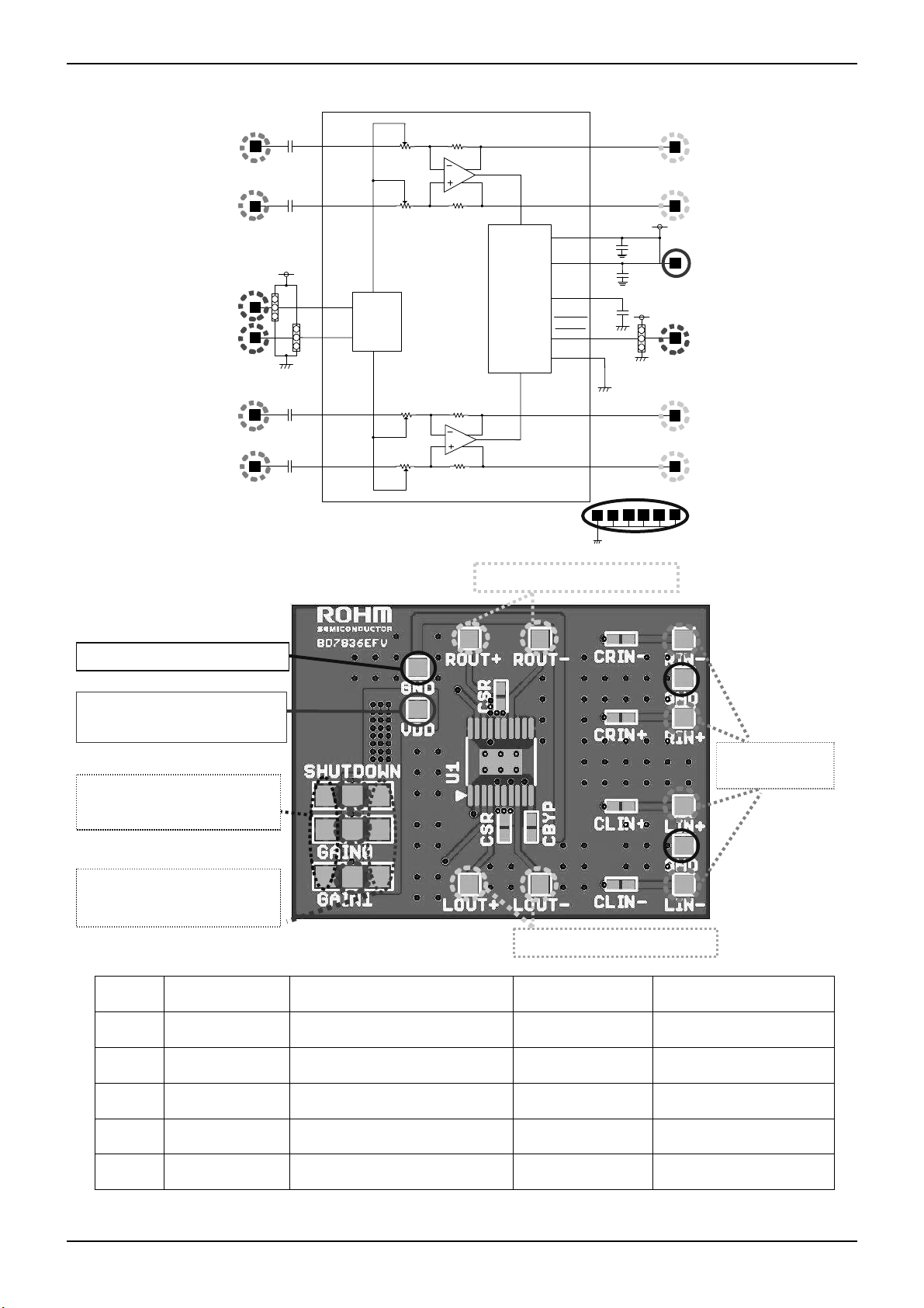
●Evaluation board circuit diagram
C
RIN-
0.47μF
C
RIN+
0.47μF
17
RIN-
+
7
RIN+
-
2
3
GAIN0
GAIN1
Gain
Control
Power
Management
C
LIN-
0.47μF
LIN-
5
C
LIN+
0.47μF
LIN+
98
+
-
Please connect speaker.
Please connect to GND.
Please connect to
Power Supply
(VDD=+4.5~5.5V) line.
Use these solder jumper
for connecting the control
terminal to GND.
Use these solder jumper
for connecting the control
terminal to VDD.
Fig .6
Please connect speaker.
●Evaluation board partts list
Number Part name Type, Value SMD size
4 CLIN+/-,CRIN+/- Capacitor, 0.47μF 1608
2 CSR Capacitor, 0.1μF 1608
1 CBYP Capacitor, 0.47μF 1608
1 U1
Class-AB stereo speaker Amplifier
1 PCB1
IC, BD7836EFV,
Printed-circuit board
BD7836EFV
PKG:HTSSOP-B20
18
ROUT+
ROUT-
14
PVDD
6.15
C
SR
0.1μF
16
VDD
BYPASS
SHUTDOWN
GND
LOUT+
LOUT-
C
SR
0.1μF
10
C
0.47μF
BYP
19
1,11,
13,20
4
GRM188R71C474KA01D
GRM188R71C104KA01D
GRM188R71C474KA01D
BD7836EFV-E2
― ―
Technical Note
Please connect ito
input signal line.
Manufacturer/
Part number
Murata
Murata
Murata
ROHM
www.rohm.com
6/16
© 2010 ROHM Co., Ltd. All rights reserved.
2010.07 - Rev.

BD7836EFV
A
Technical Note
●Description of external parts
①Input coupling capacitors Ci (CLIN+/-,CRIN+/-)
It sets cutoff frequency fc by the following formula by input coupling capacitors Ci(CLIN+/-,CRIN+/-) and input impedance Zi.
fc
1
[Hz]
CiiZ2π
It makes an input coupling capacitors of evaluation board 0.47μF on evaluation board..
Input impedance Zi and cutoff frequency fc in each gain settings are given in Table1.
Table1. The relations in the gain settings and cutoff frequency fc.
GAIN0 GAIN1 Gain [dB] Ri Ω] Zi [Ω] fc [Hz]
Lo Lo 6 90k 45k 7.5
Lo Hi 12 70k 35k 9.7
Hi Lo 18 45k 22.5k 15
Hi Hi 24 25k 12.5k 27
②The power decoupling capacitors (C
SR
)
It makes a power decoupling capacitors 0.1μF. Because power decoupling capacitors influences total harmonic distortion
(THD) and some audio characteristics, please place a good low equivalent-series-resistance (ESR) capacitors as close
as possible to IC.
③BYPASS capacitor (C
BYP
)
Because BYPASS capacitor influences THD, PSRR and some audio characteristics, please place good low
equivalent-series-resistance (ESR) capacitor as close as possible to IC.
The value of BYPASS capacitor determines the turn on time and turn off time.
Refer to the following section of “Turn ON and Turn OFF”.
It makes BYPASS capacitor of evaluation board 0.47μF.
④Control terminal
Each control terminal (
SHUTDOWN
, GAIN0, GAIN1) don’t have pull-down resistance internal circuit.
Connect to GND line or VDD line or input Low or high level voltage to terminals in order to avoid the terminals
made high Impedance.
Using IC under the control terminal let high impedance, operation fault may occur.
www.rohm.com
7/16
© 2010 ROHM Co., Ltd. All rights reserved.
2010.07 - Rev.

BD7836EFV
A
●Evaluation board PCB layer
Technical Note
Fig.7 Top layer
Fig.8 Bottom Layer
www.rohm.com
8/16
© 2010 ROHM Co., Ltd. All rights reserved.
2010.07 - Rev.

BD7836EFV
A
●Turn on and Turn off
This IC has the circuit that reduces pop noise at “turn on” and “turn off”.
Reducing pop noise is realized in controlling to adjust the turn on and turn off time.
(a)Turn ON (b)Turn OFF
The following table show the Turn ON time and Turn OFF time when It makes the BYPASS capacitor 0.47uF.
Turn ON time Turn OFF time
SHUTDOWN
5V/div.
BYPASS
1V/div.
LOUT1V/div.
Fig. 9
Technical Note
CBYP Turn ON Turn OFF
0.47uF 280ms 340ms
Turn ON time is defined as the time until BYPASS terminal voltage reaches the 90% of VDD/2 after
Turn OFF time is defined as the time until BYPASS terminal voltage reaches the 10% of VDD/2 after
The values of above table are typical characteristics. These values will shift by 30% at some conditions.
●Input terminal
This IC can be inputed signal by differntial inputs or single ended inputs.
When sing the single ended inputs, connect the terminal of not signal inputed line to AC GND with input couppling
capacitors.
Please makes the value of all input capacitors same because of preventing pop noise.
If they are not same value, for example, LOUT+=0.47µF, LOUT-=0.33µF, it caused pop noise increase and characteristics
become worse.
SHUTDOWN
SHUTDOWN H→L.
L→H.
www.rohm.com
9/16
© 2010 ROHM Co., Ltd. All rights reserved.
2010.07 - Rev.

BD7836EFV
A
Technical Note
●About the thermal design by the IC
Characteristics of an IC have a great deal to do with the temperature at which it is used, and exceeding absolute maximum
ratings may degrade and destroy elements. Careful consideration must be given to the heat of the IC from the two
standpoints of immediate damage and long-term reliability of operation. Pay attention to points such as the following.
Since an maximum junction temperature (Tj
.)or operating temperature range (Topr) is shown in the absolute maximum
MAX
ratings of the IC, to reference the value, find it using the Pd-Ta characteristic (temperature derating curve).
If an input signal is too great when there is insufficient radiation, TSD (thermal shutdown) may operate.
TSD, which operates at a chip temperature of approximately +180℃, is canceled when this goes below approximately
+100℃.
Since TSD operates persistently with the purpose of preventing chip damage, be aware that long-term use in the vicinity
that TSD affects decrease IC reliability.
Temperature Derating Curve
3.5
3.2
④3.2W
HTSSOP-B20
Measurement conditions: IC unit Rohm standard board mounted
: 70mm×70mm×1.6mmt
Board
① FR4 1-layer glass epoxy board (Copper on top layer 0%)
board
② FR4 2-layer glass epoxy board (Copper on top layer 0%)
board
③ FR4 3-layer glass epoxy board (Copper on top layer 100%)
board
④ FR4 4-layer glass epoxy board (Copper on top layer 100%)
board
2.5
2.3
③2.3W
2.0
Power dissipation Pd(W)
1.5
1.0
0.5
②1.45W
①1W
Note) Values are actual measurements and are not guaranteed.
0.0
0 25 50 75 100 125
85
Ambient Temperature Ta(℃)
150
Fig.10 Power dissipation vs. Ambient temperature
Power dissipation values vary according to the board on which the IC is mounted. The Power dissipation of this IC when
mounted on a multilayer board designed to radiate is greater than the values in the graph above.
www.rohm.com
10/16
© 2010 ROHM Co., Ltd. All rights reserved.
2010.07 - Rev.

BD7836EFV
A
●Typical Characteristics
TABLE OF GRAPHS
Technical Note
Items Parameter Figure number
Total harmonic distortion plus noise (THD+N)
Supply current (Icc)
Shutdown current (Isd)
Gain
Crosstalk
Supply ripple rejection ratio
Shutdown attenuation
Power dissipation
Efficiency
Output power
vs. Frequency 11, 12, 17, 18
vs. Output power 13, 14, 15, 16, 19, 20, 21, 22
vs. Supply voltage 23
vs. Supply voltage 24
vs. Frequency 25
vs. Frequency 26
vs. Frequency 27
vs. Frequency 28
vs. Output power 29
vs. Output power 30
vs. Load resistance 31
www.rohm.com
11/16
© 2010 ROHM Co., Ltd. All rights reserved.
2010.07 - Rev.

BD7836EFV
A
Technical Note
10
THD+N vs Frequency VDD=5V, RL=4Ω
1
400Hz-30kHz
Po=0.5W
Po=1W
Po=1.5W
THD+N vs Frequency VDD=5V, RL=4Ω, Po=1.5W
10
1
400Hz-30kHz
6dB
10dB
15.6dB
21.6dB
THD+N [%]
0.1
THD+N [%]
0.1
0.01
10 100 1k 10k 100k
Frequency [Hz]
Fig.11
Figure.1 Figure.2
0.01
10 100 1k 10k 100k
Frequency [Hz]
Fig.12
10
THD+N vs Output power VDD=5V, RL=4Ω
Gv=6dB, f=1kHz, 400Hz-30kHz
f=100Hz (30kHz LPF)
f=1kHz (400Hz-30kHz)
1
f=10kHz (80kHz LPF)
THD+N vs Output power VDD-5V, RL=4Ω
10
1
Gv=10dB, f=1kHz, 400Hz-30kHz
f=100Hz (30kHz LPF)
f=1kHz (400Hz-30kHz)
f=10kHz (80kHz LPF)
0.1
THD+N [%]
THD+N [%]
0.1
0.01
0.01 0.1 1 10
THD+N vs Output power VDD=5V, RL=4Ω
10
Output power [W]
Fig.13
Figure.3 Figure.4
Gv=15.6dB, f=1kHz, 400Hz-30kHz
0.01
0.01 0.1 1 10
Output power [W]
Fig.14
THD+N vs Output power VDD=5V, RL=4Ω
10
Gv=21.6dB, f=1kHz, 400Hz-30kHz
1
1
THD+N [%]
0.1
0.01
0.01 0.1 1 10
Output power [W]
Fig.15
Figure.5 Figure.6
THD+N vs Frequency VDD=5V, RL=8Ω, Po=1W
10
Po=0.25W
Po=0.5W
1
Po=1W
400Hz-30kHz
f=100Hz (30kHz LPF)
f=1kHz (400Hz-30kHz)
f=10kHz (80kHz LPF)
THD+N [%]
0.1
0.01
0.01 0.1 1 10
Output power [W]
f=100Hz (30kHz LPF)
f=1kHz (400Hz-30kHz)
f=10kHz (80kHz LPF)
Fig.16
THD+N vs Frequency VDD=5V, RL=8Ω, Po=1W
10
1
6dB
10dB
15.6dB
21.6dB
400Hz-30kHz
0.1
THD+N [%]
0.1
THD+N [%]
0.01
10 100 1k 10k 100k
Frequency [Hz]
Fig.17
Figure.7 Figure.8
0.01
10 100 1k 10k 100k
Frequency [Hz]
Fig.18
www.rohm.com
12/16
© 2010 ROHM Co., Ltd. All rights reserved.
2010.07 - Rev.
BD7836EFV
A
Technical Note
THD+N vs Output power VDD=5V, RL=8Ω
10
1
Gv=6dB, f=1kHz, 400Hz-30kHz
f=100Hz (30kHz LPF)
f=1kHz (400Hz-30kHz)
f=10kHz (80kHz LPF)
THD+N vs Output power VDD=5V, RL=8Ω
Gv=10dB, f=1kHz, 400Hz-30kHz
10
1
f=100Hz (30kHz LPF)
f=1kHz (400Hz-30kHz)
f=10kHz (80kHz LPF)
THD+N [%]
0.1
0.1
THD+N [%]
0.01
0.01 0.1 1 10
Output power [W]
Fig.19
Figure.9 Figure.10
0.01
0.01 0.1 1 10
Outpupower [W]
Fig.20
THD+N vs Output power VDD-5V, RL=8Ω
10
1
Gv=15.6dB, f=1kHz, 400Hz-30kHz
f=100Hz (30kHz LPF)
f=1kHz (400Hz-30kHz)
f=10kHz (80kHz LPF)
THD+N vs Output power VDD-5V, RL=8Ω
10
1
Gv=21.6dB, f=1kHz, 400Hz-30kHz
THD+N [%]
0.1
0.01
0.01 0.1 1 10
10
9
8
7
6
5
4
Icc [mA]
3
2
1
0
0123456
Gain vs Frequency VDD=5V, RL=8Ω
35
30
25
20
15
gain [dB]
10
5
0
10 100 1k 10k 100k
Outpu power [W]
Fig.21
Figure.11 Figure.12
Icc-VDD
Noload, No signal
VDD [V]
Fig.23
Figure.13 Figure.14
10Hz-500kHz
6dB
10dB
15.6dB
21.6dB
Frequency [Hz]
Fig.25
Figure.15 Figure.16
THD+N [%]
0.1
0.01
0.01 0.1 1 10
Output power [W]
f=100Hz (30kHz LPF)
f=1kHz (400Hz-30kHz)
f=10kHz (80kHz LPF)
Fig.22
Isd vs VDD
0.5
0.4
0.3
Icd [uA]
0.2
0.1
0
0123456
Noload, No signal
VDD[V]
Fig.24
Cross talk vs Frequency VDD=5V, RL=8Ω,
0
-20
-40
-60
gain [dB]
-80
-100
-120
10 100 1k 10k 100k
Left to Right
Right to Left
Gv=6dB
80kHz LPF
Frequency [Hz]
Fig.26
www.rohm.com
13/16
© 2010 ROHM Co., Ltd. All rights reserved.
2010.07 - Rev.

BD7836EFV
A
Technical Note
-20
-40
-60
PSRR [dB]
-80
-100
-120
Power Dissipation [W]
PSRR vs Frequency VDD-5V, RL=8
Vripple=0.2Vpp, 10Hz-500kHz Bandpass
0
10 100 1k 10k 100k
2
1.8
1.6
1.4
1.2
1
0.8
0.6
0.4
0.2
0
00.511.522.5
3.5
3
2.5
2
1.5
Output power[%]
1
0.5
0
0 8 16 24 32 40 48 56 64
Ω,CBYP=0.47uF
6dB
10dB
15.6dB
21.6dB
Frequency [Hz]
Figure.17 Figure.18
Fig.27
Output power vs Power Dissipation
VDD=5V, Gv=6dB, f=1kHz
Output power [W]
Fig.29
Figure.19 Figure.20
Output power vs Load Resisitance
VDD=5V, Gv=6dB, f=1kHz
THD=1%
THD=10%
Load Resistance[Ω]
RL=8Ω
RL=4Ω
RL=3Ω
SHUTDOWN attenuation vs Frequency VDD=5V
RL=8Ω, Vin=1Vrms(2Vrms@BTL), 10Hz-500kHz
0
-20
-40
-60
-80
-100
SHUTDOWN attnuation [dB]
-120
10 100 1k 10k 100k
Frequency [Hz]
Fig.28
Output power vs Efficiency
VDD=5V, Gv=6dB, f=1kHz
100
90
80
70
60
50
40
Efficiency [%]
30
20
10
0
00.511.522.5
Outputpower [W]
RL=8Ω
RL=4Ω
RL=3Ω
Fig.30
Fig.31
Figure.20
www.rohm.com
14/16
© 2010 ROHM Co., Ltd. All rights reserved.
2010.07 - Rev.

BD7836EFV
A
●Notes for use
(1) Absolute maximum ratings
This IC may be damaged if the absolute maximum ratings for the applied voltage, temperature range, or other
parameters
are exceeded. Therefore, avoid using a voltage or temperature that exceeds the absolute maximum ratings.
if it is possible that absolute maximum ratings will be exceeded, use fuses or other physical safety measures and
determine ways to avoid exceeding the IC’s absolute maximum ratings.
(2) GND terminal’s potential
Try to set the minimum voltage for GND terminal’s potential, regardless of the operation mode.
(3) Shorting between pins and mounting errors
When mounting the IC chip on a board, be very careful to set the chip’s orientation and position precisely.
When the power is turned on, the IC may be damaged if it is not mounted correctly.
The IC may also be damaged if a short occurs (due to a foreign object, etc.) between two pins, between a pin and the
power supply, or between a pin and the GND.
(4) Operation in strong magnetic fields
Note with caution that operation faults may occur when this IC operates in a strong magnetic field.
(5) Thermal design
Ensure sufficient margins to the thermal design by taking in to account the allowable power dissipation during actual use
modes, because this IC is power amp. When excessive signal inputs which the heat dissipation is insufficient condition, it
is possible that thermal shutdown circuit is active
(6) Thermal shutdown circuit
This product is provided with a built-in thermal shutdown circuit. When the thermal shutdown circuit operates, the output
transistors are placed under open status. The thermal shutdown circuit is primarily intended to shutdown the IC avoiding
thermal runaway under abnormal conditions with a chip temperature exceeding Tjmax = +150℃, and is not intended to
protect and secure an electrical appliance
(7) Load of the output terminal
This IC corresponds to dynamic speaker load, and doesn't correspond to the load except for dynamic speakers.
(8) The short protection of the output terminal
This IC has short protection circuit. The function protects the IC from rash current on road.
(9) Operating ranges
The rated operating power supply voltage range (VDD=+4.5V~+5.5V) and the rated operating temperature range
(Ta=-40℃~+85℃) are the range by which basic circuit functions is operated. Characteristics and rated output power are
not guaranteed in all power supply voltage ranges or temperature ranges.
(10) Electrical characteristics
Electrical characteristics show the typical performance of device and depend on board layout, parts, power supply.
The standard value is in mounting device and parts on surface of ROHM’s board directly.
(11) Maximum output power
When stereo inputs at R
Ensure sufficient margins to the thermal design to get larger output power.
=4Ω, maximum output power may not achieve up to typical value because the device heats.
L
Technical Note
www.rohm.com
15/16
© 2010 ROHM Co., Ltd. All rights reserved.
2010.07 - Rev.

BD7836EFV
A
●Ordering part number
B D 7 8 3 6 E F V - E 2
Part No. Part No.
HTSSOP-B20
(MAX 6.85 include BURR)
4.4±0.1
6.4±0.2
110
0.325
1.0MAX
0.85±0.05
0.65
0.08±0.05
6.5±0.1
(4.0)
7836
1120
+0.05
0.24
-
0.04
(2.4)
0.08 S
1.0±0.2
0.5±0.15
+0.05
0.17
-
S
0.03
(Unit : mm)
Package
EFV:HTSSOP-B20
<Tape and Reel information>
Embossed carrier tape (with dry pack)Tape
Quantity
Direction
of feed
2500pcs
E2
The direction is the 1pin of product is at the upper left when you hold
()
reel on the left hand and you pull out the tape on the right hand
Reel
Packaging and forming specification
E2: Embossed tape ad reel
1pin
Order quantity needs to be multiple of the minimum quantity.
∗
Technical Note
Direction of feed
www.rohm.com
16/16
© 2010 ROHM Co., Ltd. All rights reserved.
2010.07 - Rev.

Notes
No copying or reproduction of this document, in part or in whole, is permitted without the
consent of ROHM Co.,Ltd.
The content specied herein is subject to change for improvement without notice.
The content specied herein is for the purpose of introducing ROHM's products (hereinafter
"Products"). If you wish to use any such Product, please be sure to refer to the specications,
which can be obtained from ROHM upon request.
Examples of application circuits, circuit constants and any other information contained herein
illustrate the standard usage and operations of the Products. The peripheral conditions must
be taken into account when designing circuits for mass production.
Great care was taken in ensuring the accuracy of the information specied in this document.
However, should you incur any damage arising from any inaccuracy or misprint of such
information, ROHM shall bear no responsibility for such damage.
The technical information specied herein is intended only to show the typical functions of and
examples of application circuits for the Products. ROHM does not grant you, explicitly or
implicitly, any license to use or exercise intellectual property or other rights held by ROHM and
other parties. ROHM shall bear no responsibility whatsoever for any dispute arising from the
use of such technical information.
Notice
The Products specied in this document are intended to be used with general-use electronic
equipment or devices (such as audio visual equipment, ofce-automation equipment, communication devices, electronic appliances and amusement devices).
The Products specied in this document are not designed to be radiation tolerant.
While ROHM always makes effor ts to enhance the quality and reliability of its Products, a
Product may fail or malfunction for a variety of reasons.
Please be sure to implement in your equipment using the Products safety measures to guard
against the possibility of physical injury, re or any other damage caused in the event of the
failure of any Product, such as derating, redundancy, re control and fail-safe designs. ROHM
shall bear no responsibility whatsoever for your use of any Product outside of the prescribed
scope or not in accordance with the instruction manual.
The Products are not designed or manufactured to be used with any equipment, device or
system which requires an extremely high level of reliability the failure or malfunction of which
may result in a direct threat to human life or create a risk of human injury (such as a medical
instrument, transportation equipment, aerospace machinery, nuclear-reactor controller, fuelcontroller or other safety device). ROHM shall bear no responsibility in any way for use of any
of the Products for the above special purposes. If a Product is intended to be used for any
such special purpose, please contact a ROHM sales representative before purchasing.
If you intend to export or ship overseas any Product or technology specied herein that may
be controlled under the Foreign Exchange and the Foreign Trade Law, you will be required to
obtain a license or permit under the Law.
Thank you for your accessing to ROHM product informations.
More detail product informations and catalogs are available, please contact us.
ROHM Customer Support System
www.rohm.com
© 2010 ROHM Co., Ltd. All rights reserved.
http://www.rohm.com/contact/
R1010
A
 Loading...