

Page 1
A
Class-AB Speaker Amplifiers
1.1W to1.5W
Monaural Speaker Amplifier
BD7830NUV
●Description
The BD7830NUV is a monaural speaker amplifier that operates at low voltage and was developed for portable navigation
and mobile audio products. When in standby mode, its current consumption is 0 µA, and since it switches quickly and quietly
from standby to ON, it is especially well suited for applications where there is frequent switching between standby and ON.
●Features
1) BTL monaural audio power amplifier
2) High power 2.25W 4Ωat Vcc=5V ,THD+N=10%
High power 1.55W 8Ω at Vcc=5V ,THD+N=10%
High power 0.77W 8Ω at Vcc=3.6V ,THD+N=10%
3) Wide operating supply voltage range: 2.4~5.5V
4) Low standby current: 0µA
5) Fast turn on/off time: 46msec
6) Built-in Fade-in/out function
7) Built-in anti-pop function
8) Built-in thermal shutdown function
9) Very small package (VSON008V2030)
●Applications
Mobile phones, Mobile electronics applications
●Absolute Maximum Ratings(Ta=+25℃)
No.10077EAT03
Parameter Symbol Ratings Unit
Supply voltage VCC 6.0 V
Power dissipation Pd 530
Storage temperature range Tstg -55~+150 ℃
STBY input range V
*1 ROHM standard one layer board (70mm×70mm×1.6mmt) mounted, deratings is done at 4.24mW/℃ above Ta=+25℃.
●Operating Range
Parameter Symbol Ratings Unit
Temperature range Topr -40~+85 ℃
Supply voltage VCC +2.4~+5.5 V
※ This product is not designed for protection against radioactive rays.
-0.1~Vcc+0.1 V
STBY
*1
mW
www.rohm.com
© 2010 ROHM Co., Ltd. All rights reserved.
1/17
2010.06 - Rev.
Page 2
A
BD7830NUV
p
●Electrical characteristics (Unless otherwise noted, Ta=+25℃, VCC=+3.0V, f=1kHz, RL=8Ω)
Parameter Symbol
MIN. TYP. MAX.
Limit
Unit
Monitor
pin
Supply current ICC ― 3.2 6.8 mA 6 Active mode
Technical Note
Condition
Standby supply current I
― 0 2 µA 6 Standby mode
STBY
Output power PO 280 420 ― mW 5&8 BTL, THD+N=1% *1
Total harmonic distortion THD+N ― 0.1 0.5 % 5&8 BTL, Po=150mW
Voltage gain1 AV1 -1 0 +1 dB 5 Vin=-20dBV, 1stAmp
Voltage gain2 AV2 -1 0 +1 dB 8 Vin=-20dBV, 2ndAmp
Power supply rejection ratio PSRR 40 57 ― dB 5&8
BTL, Vripple=0.2Vpp *2
Mute attenuation MUTE 60 80 ― dB 5&8 BTL, Vin=-20dBV
Output voltage Vo 1.35 1.5 1.65 V 5&8 Vin=0V
Output offset voltage ΔVo -40 0 +40 mV 5&8 ΔVo=|Vo1-Vo2 |
STBY release voltage V
STBY hold voltage V
STBY input current H I
STBY input current L I
*1:B.W.=400~30kHz, *2:DIN AUDIO, SE:Single End, BTL:The voltage between 5pin and 8pin
1.4 ― Vcc+0.1 V 1 Active mode
STBYH
-0.1 ― 0.4 V 1 Standby mode
STBYL
20 30 40 µA 1 V
STBYH
-2 0 ― µA 1 V
STBYL
STBY
STBY
=3V
=0V
●Application Circuit Example
Audio
In
ut
H : ACTIVE
L : STBY
1μF
VCC
1
2
0.01uF
0.1uF
20kΩ
STB
SOFT
?
BIAS
IN-
OUT2
1
2
Bias
2ndAmp
3
SOFT
4
1stAmp
8
GND
7
V
DD
6
OUT1
5
8Ω
1μF
※3pin SOFT terminal
1 : Usually
2 : Enable to adjust fade in/out time
by external capacitor
20kΩ
*1
www.rohm.com
© 2010 ROHM Co., Ltd. All rights reserved.
2/17
2010.06 - Rev.
Page 3
BD7830NUV
●Outer dimension
D78
30
●Reference land pattern (adapt as necessary to suit conditions during actual design.)
PKG type
Unit: mm
L2
VSON008V2030 0.50 2.20 0.70 0.27
D3
MD1
E3
※ This package is a non-lead type, so solderability of the lead ends and sides are
PKG type
VSON008V2030 1.20 1.60 ― φ0.300
not guaranteed.
b2 e
Thermal via
Technical Note
Lead pitch
Gap Length Width
e MD1 L2 b2
Central pad Thermal via
Length Width
D3 E3
Land
Pitch Diameter
www.rohm.com
© 2010 ROHM Co., Ltd. All rights reserved.
3/17
2010.06 - Rev.A
Page 4
BD7830NUV
●Measurement Circuit Diagram
VSTBY
STBY
A
1
OUT2
8
V
GND
7
VCC
6
OUT1
100μ
600
8
Vri pp l e
50
VCC
A
1μ
V
0.1μ
1
2
20k
BIAS
1μ
SOFT
Bias
2
2nd Amp
SOFT
3
IN-
4 5
1st Amp
Vin
VCC
0.01μ
600
※3pin SOFT terminal
1 : Usually
2 : Enable to adjust fade in/out time
by external capacitor
20k
●Block diagram ●Pin assignment
STBY
1
OUT2
8
BIAS
2
Bias
GND
7
PIN No. PIN Name
1 STBY
2 BIAS
3 SOFT
SOFT
SOFT
3
2nd
VCC
6
IN-
4 5
1st Amp
OUT1
4 IN-
5 OUT1
6 VCC
7 GND
8 OUT2
Technical Note
www.rohm.com
© 2010 ROHM Co., Ltd. All rights reserved.
4/17
2010.06 - Rev.A
Page 5
BD7830NUV
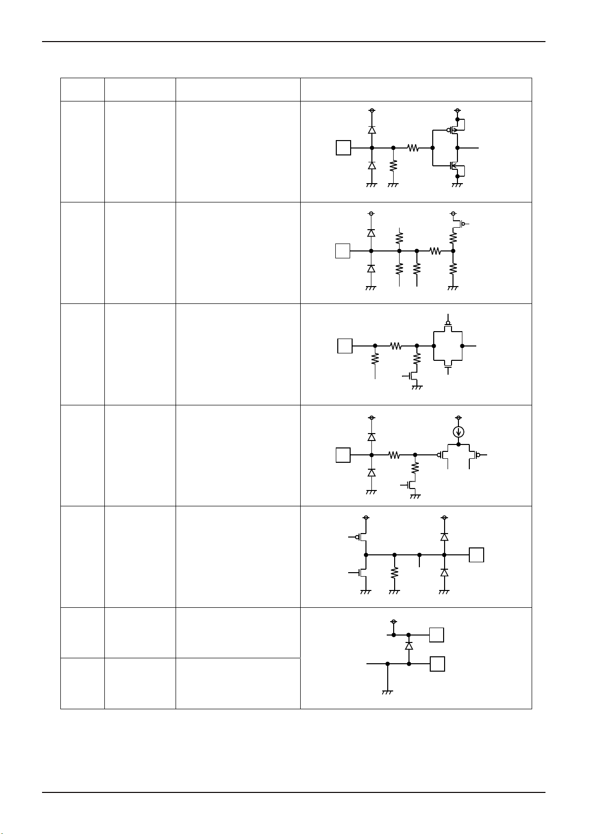
●Input/output equivalent circuit
PIN No. PIN Name PIN description Equivalent circuit
Technical Note
Active/Standby
1 STBY
Control pin
STBY=H → Active
STBY=L → Standby
2 BIAS
3 SOFT
Bias capacitor
Connection pin
Fade-in/out
Adjustment pin
STBY
1
BIAS
2
SOFT
3
10k
25k
1k
100k
50k
600k
1k 20k
100k
100k
IN-
4 IN- Input pin
5
8
OUT1
OUT2
Output pin
4
6 VCC Power supply pin
7 GND GND pin
Notes) The above numerical values are typical values for the design, which are not guaranteed.
1k
1k
OUT1
(OUT2)
5
60k
(8)
VCC
6
7
GND
www.rohm.com
© 2010 ROHM Co., Ltd. All rights reserved.
5/17
2010.06 - Rev.A
Page 6
BD7830NUV
Technical Note
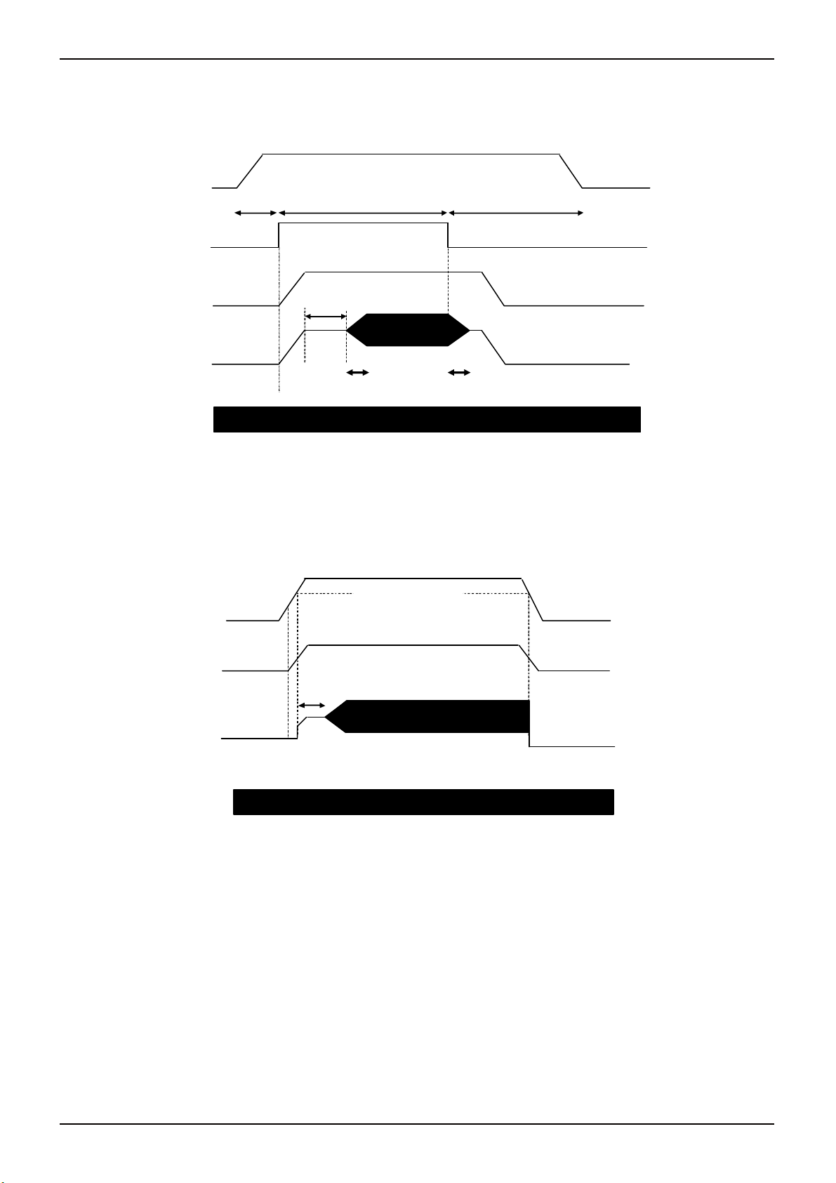
●Description of operations
①ON/OFF operation by STBY pin
VCC
Standby
Active Standby
STBY
BIAS
Delay
(i nterna lly
OUT
Audio
Input
FADE IN
FADE OUT
Normal input
mode
Once VCC = H, when STBY = L → H then BIAS and output (OUT) are activated.
Once BIAS has become stable (= 1/2 VCC), output (OUT) fades in (FADE IN).
Once STBY = H → L, output (OUT) starts to fade out (FADE OUT), and when fade-out ends, the BIAS falls.
②ON/OFF control by shorting of VCC and STBY pins
VCC
STBY
Under voltage
protection
1.78V (typ)
BIAS
Delay
(internal ly fixed)
OUT
Audio
Input
When VCC = STBY = L → H, BIAS is activated. During low power mode (VCC < 1.78 V) protection is used to keep output
(OUT) at low level, and FADE IN occurs when this protection is canceled. When VCC = STBY = H → L, output (OUT) falls
without FADE OUT.
www.rohm.com
© 2010 ROHM Co., Ltd. All rights reserved.
6/17
2010.06 - Rev.A
Page 7
BD7830NUV
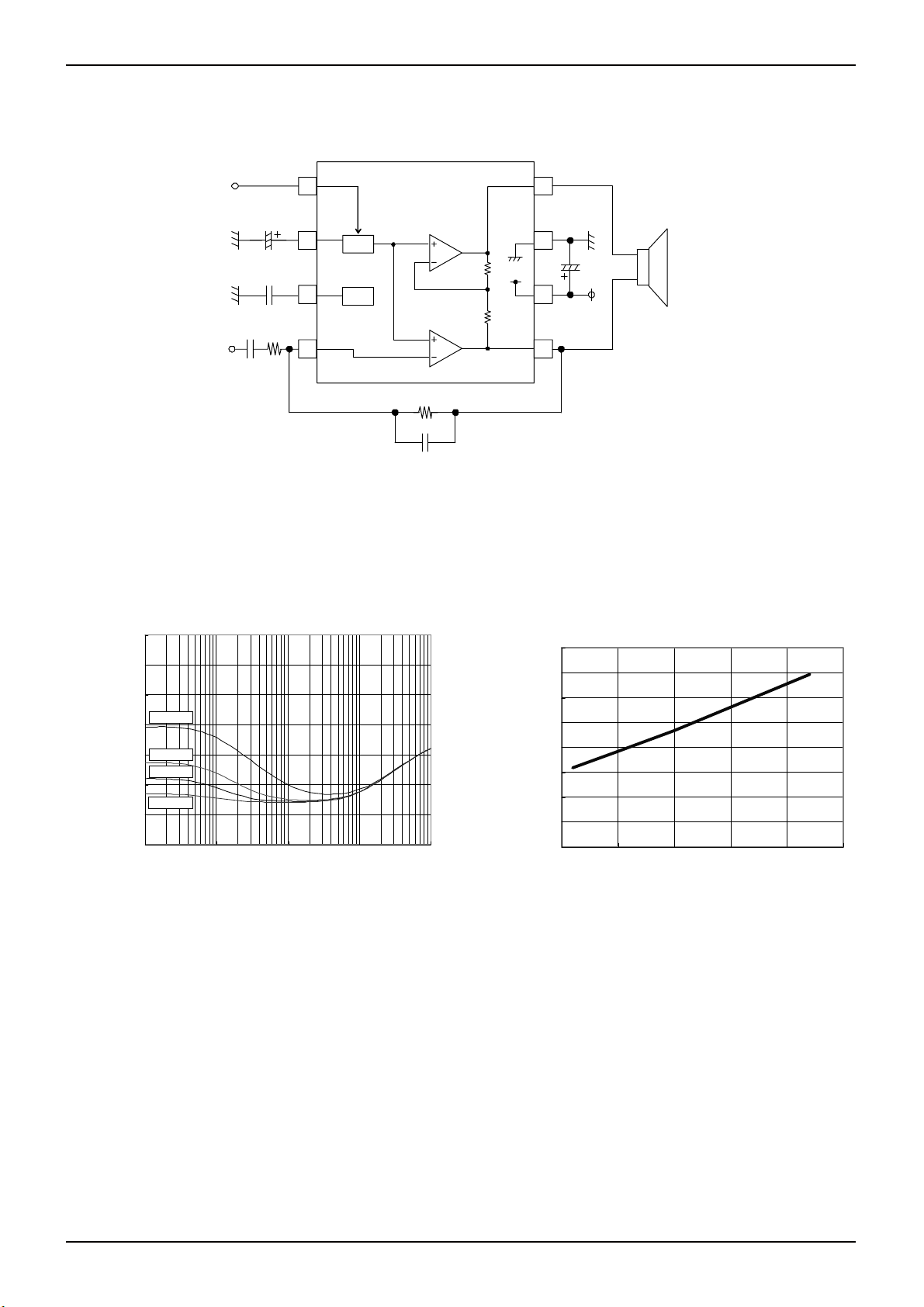
●External components and cautions points
Setting of external components
STBY
STBY
1
OUT 2
8
SP_IN
BIAS
2
Cb
SOFT
Cs
IN-
Ci
Ri
Bias
2ndAmp
3
SOFT
4 5
1stAmp
GND
7
1μ
VCC
6
OUT 1
Rf
Cf
●Cb
This is a bypass capacitor, which is used for bias voltage stabilization.
When a larger capacitor is used, the efficiency of voltage ripple rejection can be improved.
When tuning, note with caution that Cb can affect the activation time.
Cb – Power Supply Ripple Rejection Ratio Cb – Turn-on Time
0
-10
-20
Cb=0.1uF
-30
Cb=0.47uF
-40
Cb=1uF
-50
Cb=2.2uF
Power Supply Rej ection Ra tio[dB]
-60
-70
10 100 1k 10k 100k
Vcc=3V, Vripple=200mVpp, RL=8Ω
Cb-PSRR
Frequency[Hz]
80
70
60
50
40
ton[ms]
30
20
10
0
0 0.5 1 1.5 2 2.5
Technical Note
SPEAKER
8Ω
Cb-ton
Cb[uF]
www.rohm.com
© 2010 ROHM Co., Ltd. All rights reserved.
7/17
2010.06 - Rev.A
Page 8

BD7830NUV
Technical Note
●Cs
This capacitor is for adjustment of the FADE IN/OUT times. The FADE IN/OUT functions soften the operation (IN and OUT)
of BTL output when switching between standby and active modes.
When a capacitor is connected to the SOFT pin (pin 3), the FADE IN/OUT functions are valid. When the capacitor
rating is increased, the FADE IN/OUT effect is also increased, but note with caution when setting this that it also affects the
activation time. If the FADE IN/OUT functions are not being used, connect the SOFT pin (pin 3) to VCC.
・ Fade-in/out waveforms
Standby → Active
Active → Standby
STBY
2V/div
BTL output
0.5V/div
Ton
To ff
140
120
100
80
60
ton,toff[ms]
40
20
0
0 0.02 0.04 0.06 0.08 0.1
Cs - Fade-in/out Time
Cs-ton,toff
ton
toff
Cs[uF]
www.rohm.com
© 2010 ROHM Co., Ltd. All rights reserved.
8/17
2010.06 - Rev.A
Page 9

BD7830NUV
Technical Note
●Ci
This is a DC cut-off input coupling capacitor for the amp input pin.
This includes an Ri and a high-pass filter. The cut-off frequency is calculated as follows.
f
= [Hz]
CL
1
2π×Ri×Ci
Ci – Low Frequency Characteristics
Ci-Frequency characteristic
4
2
0
-2
Gain [dB]
-4
-6
-8
-10
10 100 1k 10k 100k
Ci:0.047uF
Ci:0.1uF
Ci:0.22uF
Frequency[Hz]
Capacitors of a certain size are required for coupling without attenuation of low frequencies, but in most cases of speakers
used in portable equipment, it is nearly impossible to reproduce signals in the 100 to 200 Hz range or below. Even when a
larger capacitor is used instead, it may not improve system performance. Also, pop sounds can affect the capacitance (Ci) of
the capacitor. A larger coupling capacitor requires a greater charge to reach the bias DC voltage (normally 1/2 VCC).
Because this charge current is supplied from the output due to routing of feedback, pop sounds occur easily at startup.
Consequently, pop sounds can be minimized by selecting the smallest capacitor that still has the required low-frequency
response.
●Ri
This is inverting input resistance, which sets the closed loop gain in conjunction with Rf.
●Rf
This is feedback resistance, which sets closed loop gain in conjunction with Rf. The amp gain is set using the following
formula.
Gain = 20log [dB]
Rf
Ri
●Cf
This is a feedback capacitor, which is used to cut high frequencies.
This includes Rf and a low-pass filter. The cut-off frequency is calculated as follows.
f
= [Hz]
CL
1
2π×Ri×Ci
www.rohm.com
© 2010 ROHM Co., Ltd. All rights reserved.
9/17
2010.06 - Rev.A
Page 10

BD7830NUV
Technical Note
●Selection of external components
①Setting gain from desired output
Output Po is determined via the following formula, from which the required gain Av can also be obtained.
Po [W] = Vo
2
[Vrms] / RL [Ω]
Vo = Av ・ Vin
RLPo
・
Av ≧
/ Vin
②Setting input resistance and feedback resistance from gain
Gain Av is determined via the following formula, from which input resistance Rin and feedback resistance Rf can be set.
Av = (Rf / Rin) ・ 2
Rin is set with the input side's drive capacity taken into account.
③Setting input coupling capacitor from low-range cut-off frequency
Low-range cut-off frequency fc is determined via the following formula, from which input coupling capacitor Cin can be set.
fc [Hz] = 1 / (2π ・ Rin ・ Cin)
Cin ≧ 1 / (2π ・ Rin ・ fc)
④Setting bias capacitor and SOFT capacitor to minimize pops
It is recommended that the capacitance of the bias capacitor CB be set to at least 10 times that of the input coupling
capacitor Cin, in order to soften the rise of the bias voltage while improving the Cin following ability.
Also, when a higher gain is used, the capacitance of the SOFT capacitor Cs can be raised to control pop sounds.
Av = 2 (6 dB at BTL) → Cs ・ (80 / fc) ≧ 0.01 µF
Av = 4 (12 dB at BTL) → Cs ・ (80 / fc) ≧ 0.022 µF
Av = 8 (18 dB at BTL) → Cs ・ (80 / fc) ≧ 0.033 µF
Av = 20 (26 dB at BTL) → Cs ・ (80 / fc) ≧ 0.068 µF
●Use when VCC = STBY short
Since this IC is designed on the assumption that it will be used to switch standby mode ON and OFF while the power supply
remains ON, normally STBY should be switched from H to L and the SOFT voltage should be discharged before powering
down. When used while VCC = STBY short, pop sounds may occur if the IC's power supply is reduced prior to discharging
the SOFT voltage.
To prevent pop sounds, you must ① set STBY = H→L before setting VCC = H→L
, and ② forcibly discharge the SOFT
voltage.
A sample circuit in which VCC = STBY short is used is shown below.
・Sample circuit configuration when VCC = STBY short
②
Fast discharge of
SOFT voltage at
power-off
Cin
STBY
1
BIAS
1μ
SOFT
CS
Rin
Bias
2
2nd Amp
SOFT
3
IN-
4 5
1st Amp
Rf
OUT2
8
GND
7
VCC
6
OUT1
CD
Slow power-off of IC itself
①
STBY = H → L at
power-off
VCC
www.rohm.com
© 2010 ROHM Co., Ltd. All rights reserved.
10/17
2010.06 - Rev.A
Page 11
BD7830NUV
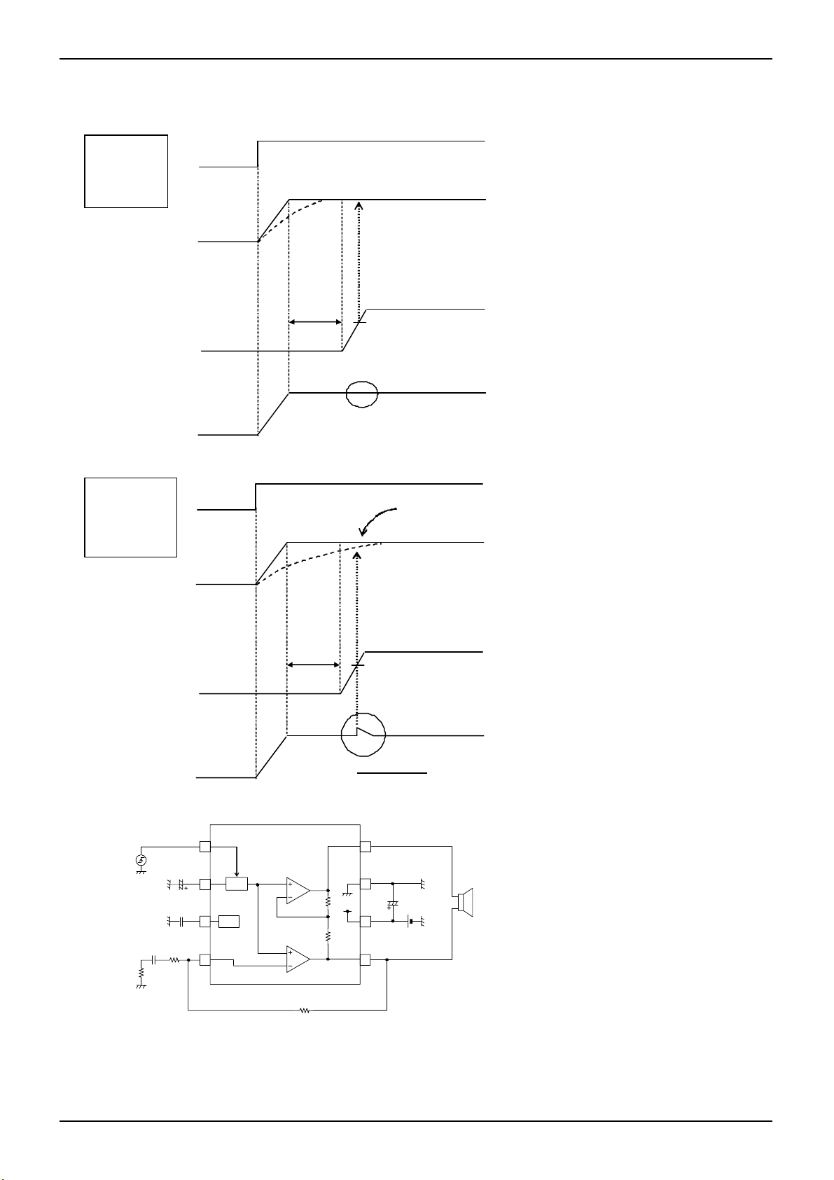
●Mechanism of pop sounds
Cin is low
Gain is low
(Rf)
STBY
BIAS
IN-
SOFT
OUT
Cin is high
Gain is high
(Rf)
STBY
BIAS
IN-
SOFT
OUT
STBY
1
600
BIAS
2
1μ
SOFT
SOFT
3
CS
Cin
IN-
4 5
Ri
Bias
BIAS
IN-
About 25
BIAS
IN-
About
25 ms
2nd Amp
1st Amp
Rf
0.6 VCC
No pops
0.6 VCC
POP sounds
OUT2
8
GND
7
1μ
VCC
6
OUT1
VCC
Potential
difference
Technical Note
When SOFT voltage reaches 0.6 VCC, if there
is a potential difference between BIAS and IN-,
pop sounds will occur.
At startup, the input coupling Cin is charged
from output OUT via the feedback resistance
Rf, so when
Cin and Rf are high, charging takes longer and
pop sounds can easily occur.
The rise of the SOFT voltage is changed by CS,
so pop sounds an be reduced by setting CS
high.
RL
www.rohm.com
© 2010 ROHM Co., Ltd. All rights reserved.
11/17
2010.06 - Rev.A
Page 12

BD7830NUV
Technical Note
●Bass boost function
External components can be added to this chip to provide a bass boost function.
Ri Ci
IN-
4
BIAS
OUT
5
Rfb
Rf
Cfb
Gain
GC1
Low fre qu e ncy gain up
f
2C
f
1C
G
C2
1C
1
RfCfb2
1
log20G
Ri
)Rfb//Rf(Cfb2
RfbRf
[Hz]
[Hz]
[dB]
f
C1 fC2
f
2C
Rf
(normal use)
log20G
Ri
[dB]
●Thermal shutdown function
When the chip exceeds the Tjmax (150°C) temperature by reaching a temperature of 180℃ or above, the protection
function is activated. High impedance is for OUT1 and OUT2 during protected mode. Protection is canceled and normal
operation is resumed when the chip's temperature falls to 120℃ or below.
Chip
180°C
120°C
Protection start temperature: 180°C (typ) or more
Protection cancels temperature: 120°C (typ) or
less
Output
Nor ma l
Protected
operation
Normal
www.rohm.com
© 2010 ROHM Co., Ltd. All rights reserved.
12/17
2010.06 - Rev.A
Page 13

BD7830NUV
Technical Note
●Thermal design of chip
The characteristics of the IC vary greatly depending on the use temperature, and when the maximum allowable junction
temperature is exceeded, components may deteriorate or become damaged. Thermal considerations are needed for this
chip from two standpoints: preventing instantaneous damage and improving long-term reliability. Note the following points
with caution.
The absolute maximum ratings for each chip include the maximum junction temperature (Tj
) and operating temperature
MAX
rate (Topr), and these values should be referred to when using the Pd-Ta characteristics (thermal dissipation curve).
Since the IC itself is designed with full consideration of thermal balance, there are no problems in terms of circuit operations,
but even when a more-than-adequate thermal design is implemented in order to get full use of the IC's performance features,
some moderation is often required for the sake of practical usage.
If there is an excessive input signal due to insufficient thermal dissipation, a TSD (thermal shutdown) operation may occur.
Thermal Dissipation Curve
The allowable loss value varies depending on the type of board used for mounting. When this chip is mounted on a
multi-layer board that is designed for thermal dissipation, the allowable loss becomes greater than shown in the above figure.
Reference data
1.0
0.5
Allowable loss Pd (W)
0
(Note) These are measured values. They are not guaranteed.
VSON008V2030
① When mounted on ROHM standard 1-layer board
Size: 70 mm × 70 mm × 1.6 mmt
No copper heat sink (only mounti ng pattern)
0.85W
② When mounted on 4-layer bo ard
Size: 76.2 mm × 76.2 mm × 1.6 mmt
Layers 2 & 3 Copper foil
No connection v ia thermal via
②
0.53W
①
0 25 50 75 100 125 150
Ambient temperature Ta (°C)
www.rohm.com
© 2010 ROHM Co., Ltd. All rights reserved.
13/17
2010.06 - Rev.A
Page 14
BD7830NUV
●Typical Characteristics (1)
BD7830NUV f-THD+N
VCC=5V ,Ta=25℃,Po=150mW,RL=8Ω
10
1
THD+N[%]
0.1
0.01
10 100 1k 10k 100k
10
BD7830NUV Po-THD
Ta=25℃,f=1kHz,RL=8Ω
1
VCC=3V
THD[%]
0.1
0.01
0.01 0.1 1 10
BD7830NUV frequency characteristic
VCC=5V,Ta=25℃,Vin=-20dBV,RL=8Ω
10
5
0
-5
Gain[dB]
-10
-15
10 100 1k 10k 100k
f[Hz]
Po[W]
f[Hz]
VCC=5V
Technical Note
BD7830NUV f-THD+N
VCC=3V,Ta=25℃,Po=150mW,RL=8Ω
10
1
THD+N[%]
0.1
0.01
10 100 1k 10k 100k
f[Hz]
Ta=25℃ f=1kH z 400~30kBPF THD+N=1.0%
10000
1000
Po[mW ]
100
23456
10
5
0
Gain[dB]
-5
-10
-15
10 100 1k 10k 100k
BD7830N UV VCC-Po
RL=4Ω
RL=8Ω
RL=16Ω
Vcc[V]
BD7830NUV frequency characteristic
VCC=3V,Ta=25℃,Vin=-20dBV,RL=8Ω
f[Hz]
www.rohm.com
© 2010 ROHM Co., Ltd. All rights reserved.
14/17
2010.06 - Rev.A
Page 15

BD7830NUV
●Typical Characteristics (2)
0
-10
-20
Ta=25℃,VCC=5V , Vripple=200mVpp,30kLPF
BD7830NUV f-PSRR
-30
-40
-50
Power Supply Rejection Ratio [dB]
-60
-70
10 100 1k 10k 100k
8
BD7830NUV Circuit current (ACT)
Ta=25℃,RL=8Ω
6
4
2
Circuit current (ACT)[mA ]
0
23456
BD7830NUV Po-Pd
0.7
0.6
0.5
0.4
Pd[W]
0.3
VCC=3V
0.2
0.1
0.0
0.0 0.5 1.0 1.5
f[Hz]
VCC[V]
VCC=5V
Po[W]
Technical Note
Ta=25℃, VCC=3V,Vripple=200mVpp,30kLPF
0
-10
-20
-30
-40
-50
Po wer S u pply R e jectio n Ratio [ dB]
-60
-70
10 100 1k 10k 100k
0.10
0.09
0.08
0.07
0.06
0.05
0.04
0.03
0.02
Circuit current ( STB Y)[μA]
0.01
0.00
23456
10.00
1.00
Po
0.10
0.01
VCC=3V
1 10 100
BD7830NUV f-PSRR
f[Hz]
BD7830NUV Circuit current (STBY)
Ta=25℃, RL=8Ω
VCC[V]
BD7830NUV RL-Po
Ta=25℃, f=1kHz, THD+N=1%
VCC=5.5 V
VCC=2.4V
RL[Ω]
www.rohm.com
© 2010 ROHM Co., Ltd. All rights reserved.
15/17
2010.06 - Rev.A
Page 16

BD7830NUV
●Notes for use
1) The above numerical values and data are typical values for the design, which are not guaranteed.
2) The application circuit examples can be reliably recommended, but their characteristics should be checked carefully
before use. When using external component constants that have been modified, determine an ample margin that takes
into consideration variation among the external components and Rohm's LSI IC chips, including variation in static
characteristics and transient characteristics.
3) Absolute maximum ratings
This IC may be damaged if the absolute maximum ratings for the applied voltage, temperature range, or other parameters
are exceeded. Therefore, avoid using a voltage or temperature that exceeds the absolute maximum ratings. If it is possible
that absolute maximum ratings will be exceeded, use fuses or other physical safety measures and determine ways to
avoid exceeding the IC's absolute maximum ratings. The above numerical values and data are typical values for the
design, which are not guaranteed.
4) GND pin's potential
Try to set the minimum voltage for GND pin's potential, regardless of the operation mode.
Check that the voltage of each pin does not go below GND pin's voltage, including transient phenomena.
5) Shorting between pins and mounting errors
When mounting the IC chip on a board, be very careful to set the chip's orientation and position precisely. When the power
is turned on, the IC may be damaged if it is not mounted correctly. The IC may also be damaged if a short occurs (due to
a foreign object, etc.) between two pins, between a pin and the power supply, or between a pin and the GND.
6) Shorting output pin
When output pin (5,8pin) is shorted to VCC or GND, the IC may be damaged by over current, so be careful in operation.
7) Thermal design
Ensure sufficient margins to the thermal design by taking in to account the allowable power dissipation during actual use
modes, because this IC is power amp.
When excessive signal inputs which the heat dissipation is insufficient condition, it is possible that TSD (thermal shutdown
circuit) is active.
TSD is protection of the heat by excessive signal inputs, it is not protection of the shorting output to VCC or GND.
8) Shorted pins and mounting errors
When the output pins (pins 5 and 8) are connected to VCC and GND, the thermal shutdown function repeatedly switches
between shutdown (OFF) and cancel (ON). Note with caution that chip damage may occur if these connections remain
for a long time.
9) Operating range
The rated operating power supply voltage range(VCC=+2.4 ~+5.5V) and the rated operation temperature range
(Ta=-40~+85℃) are the range by which basic circuit functions is operated.
It is not guaranteed a specification and a rated output power about all operating power supply voltage range or operation
temperature range.
10) Operation in strong magnetic fields
Note with caution that operation faults may occur when this IC operates in a strong magnetic field.
Technical Note
www.rohm.com
© 2010 ROHM Co., Ltd. All rights reserved.
16/17
2010.06 - Rev.A
Page 17

BD7830NUV
●Ordering part number
B D 7 8 3 0 N U V - T R
Technical Note
Part No. Part No. Package
VSON008V2030
2.0±0.1
0.08 S
C0.25
1.0MAX
0.3±0.1
0.25
1.5±0.1
0.5
3.0±0.1
1PIN MARK
0.02
-
+0.03
0.02
4
1.4±0.1
518
+0.05
0.25
-
0.04
S
(0.22)
(Unit : mm)
NUV:VSON008V2030
<Tape and Reel information>
Embossed carrier tapeTape
Quantity
Direction
of feed
3000pcs
TR
The direction is the 1pin of product is at the upper right when you hold
()
reel on the left hand and you pull out the tape on the right hand
Reel
Packaging and forming specification
TR: Embossed tape and reel
1pin
Order quantity needs to be multiple of the minimum quantity.
∗
Direction of feed
www.rohm.com
© 2010 ROHM Co., Ltd. All rights reserved.
17/17
2010.06 - Rev.A
Page 18

Notes
No copying or reproduction of this document, in par t or in whole, is permitted without the
consent of ROHM Co.,Ltd.
The content specied herein is subject to change for improvement without notice.
The content specied herein is for the purpose of introducing ROHM's products (hereinafter
"Products"). If you wish to use any such Product, please be sure to refer to the specications,
which can be obtained from ROHM upon request.
Examples of application circuits, circuit constants and any other information contained herein
illustrate the standard usage and operations of the Products. The peripheral conditions must
be taken into account when designing circuits for mass production.
Great care was taken in ensuring the accuracy of the information specied in this document.
However, should you incur any damage arising from any inaccuracy or misprint of such
information, ROHM shall bear no responsibility for such damage.
The technical information specied herein is intended only to show the typical functions of and
examples of application circuits for the Products. ROHM does not grant you, explicitly or
implicitly, any license to use or exercise intellectual property or other rights held by ROHM and
other parties. ROHM shall bear no responsibility whatsoever for any dispute arising from the
use of such technical information.
Notice
The Products specied in this document are intended to be used with general-use electronic
equipment or devices (such as audio visual equipment, ofce-automation equipment, communication devices, electronic appliances and amusement devices).
The Products specied in this document are not designed to be radiation tolerant.
While ROHM always makes efforts to enhance the quality and reliability of its Products, a
Product may fail or malfunction for a variety of reasons.
Please be sure to implement in your equipment using the Products safety measures to guard
against the possibility of physical injury, re or any other damage caused in the event of the
failure of any Product, such as derating, redundancy, re control and fail-safe designs. ROHM
shall bear no responsibility whatsoever for your use of any Product outside of the prescribed
scope or not in accordance with the instruction manual.
The Products are not designed or manufactured to be used with any equipment, device or
system which requires an extremely high level of reliability the failure or malfunction of which
may result in a direct threat to human life or create a risk of human injur y (such as a medical
instrument, transportation equipment, aerospace machinery, nuclear-reactor controller, fuelcontroller or other safety device). ROHM shall bear no responsibility in any way for use of any
of the Products for the above special purposes. If a Product is intended to be used for any
such special purpose, please contact a ROHM sales representative before purchasing.
If you intend to export or ship overseas any Product or technology specied herein that may
be controlled under the Foreign Exchange and the Foreign Trade Law, you will be required to
obtain a license or permit under the Law.
Thank you for your accessing to ROHM product informations.
More detail product informations and catalogs are available, please contact us.
ROHM Customer Support System
www.rohm.com
© 2010 ROHM Co., Ltd. All rights reserved.
http://www.rohm.com/contact/
R1010
A
 Loading...