

Page 1

System Motor Driver ICs for CD / DVD / Blu-ray Drive and Recorder
System Motor Driver IC
for Half Height Drive (Sensor less)
BD7755RFV
●Description
BD7755RFV are ICs, developed for the spindle motor, actuator coil, tilt coil, stepping motor, SA stepping motor and the
loading motor drive of the desktop Blu-ray drive and Blu-ray recorder. Spindle driver adopted sensorless drive system, and
the hall sensor (3 pieces) of the motor position detection is not needed, it is suitable for making of flexible cable conserve
wiring and the reductions of external parts. The low rotation mode is built in, and stability and low-speed a rotation is
achieved. The spindle, stepping and SA stepping use power MOSFET to reduce power consumption and the actuator, tilt,
and loading driver use a linear BTL drive system to reduce noise.
●Features
1) The low-speed stability rotation is achieved with built-in the low rotation mode.
2) The hall sensor is unnecessary according to 3 aspect sensorless drive system.
3) The spindle motor driver achieves stability high speed start by ROHM's own energizing method.
4) Highly effective spindle, stepping and SA stepping is achieved by PWM control driver. And the output current detection
resistance of stepping and SA stepping is unnecessary by built-in internal detection circuit.
5) The actuator, tilt and loading driver achieve low noise by using linear BTL drive system.
6) ON/OFF of loading and other channels, brake mode of spindle driver and standby mode are selectable by the two
control terminals.
7) Built-in thermal-shut down circuit.
8) Improved heat radiation efficiency utilizing HTSSOP package.
●Applications
For desktop Blu-ray drive
●Absolute maximum ratings
No.10012EAT01
Parameter Symbol Ratings Unit
POWER MOS power supply voltage 1 SPVM, SLVM 15
POWER MOS power supply voltage 2 SAVM 7
Preblock/BTL power block power supply voltage Vcc, AVM, LDVM 15
PWM control block power supply voltage DVcc 7
Power dissipation Pd 1.5
Operating temperature range Topr -20 ~ 70
Storage temperature Tstg -55 ~ 150
Junction temperature Tjmax 150
#1 POWER MOS output terminals (40~43pin, 46~48pin) are contained.
#2 POWER MOS output terminals (35~38pin) are contained.
#3 PCB mounting (70mmX70mmX1.6mm, occupied copper foil is less than 3%, glass epoxy standard board).
Reduce by 12mW/℃ over 25℃
#1
#2
#3
V
V
V
V
W
℃
℃
℃
www.rohm.com
© 2010 ROHM Co., Ltd. All rights reserved.
1/18
2010.06 - Rev.A
Page 2

BD7755RFV
Technical Note
●Recommended operating conditions
(Set the power supply voltage with consideration to power dissipation)
Parameter Symbol
Spindle / Sled motor driver power block power
supply voltage
Min. Typ. Max.
SPVM,SLVM - Vcc
Ratings
#4
- V
Pre block power supply voltage Vcc 10.8 12 13.2 V
Loading driver power block supply voltage LDVM 4.3 5.0 Vcc V
Unit
SA, Actuator driver power block
power supply voltage
SAVM,AVM 4.3 5.0 5.5 V
PWM control block power supply voltage DVcc 4.3 5.0 5.5 V
Spindle driver output current Iosp - 1.0 2.5 #5A
Actuator, SA, sled, loading motor driver
output current
#4 Set the same supply voltage to SPVM, SLVM and Vcc.
#5 The current is guaranteed 3.5A in case of the Short-circuit braking mode and the current which is turned on/off in
a duty-ratio of less than 1/10 with a maximum on-time of 5msec
Ioo - 0.5 0.8 A
www.rohm.com
© 2010 ROHM Co., Ltd. All rights reserved.
2/18
2010.06 - Rev.A
Page 3

BD7755RFV
●Electrical characteristics
(Unless otherwise noted, Ta=25℃, Vcc=SPVM=SLVM=12V, DVcc=AVM=SAVM= LDVM=5V, Vc=1.65V,RL=8Ω,RLSP=2Ω)
Parameter Symbol
Circuit current
Quiescent current 1 IQ1 - 14 30 mA Vcc(Loading OFF)
Quiescent current 2 IQ2 - 7.5 16 mA Vcc(Loading ON)
Quiescent current 3 IQ3 - 7 14 mA DVcc
Standby-on current 1 IST1 - 1.1 2.4 mA Vcc
Standby-on current 2 IST2 - 0.16 0.4 mA DVcc
Sled driver block
Input dead zone (one side) VDZSL 0 30 80 mV
Input output gain gmSL 0.75 1.0 1.25 A/V
Output On resistor
(top and bottom)
Output limit current ILIMSL 0.8 1.1 1.4 A
PWM frequency fosc - 100 - kHz
Spindle driver block<Torque instruction input / output>
Input dead zone (one side)1 VDZSP1 20 55 90 mV VLRPM=L
Input dead zone (one side)2 VDZSP2 20 240 450 mV VLRPM=H
Input output gain 'H' gmSPH 2.68 3.5 4.32 A/V VLRPM=L
Input output gain 'L' gmSPL 0.53 0.7 0.87 A/V VLRPM=H
Output On resistor (top and bottom) RONSP - 1.0 1.7 Ω IL=500mA
Output limit current ILIMSP 1.35 1.6 1.85 A RSPLIM=1.5kΩ
PWM frequency fosc - 167 - kHz
FG output, PRTFLG output
High voltage VOH - 4.9 - V 100kΩ pull up to DVcc
Low voltage VOL - 0.1 - V
Focus / Tracking / Tilt driver block
Output offset voltage VOFA -50 0 50 mV
Output saturation voltage (top and bottom) VOHA - 0.9 1.8 V IL=500mA
Voltage gain H GVAH 19.6 21.6 23.6 dB VLRPM=L
Voltage gain L GVAL 13.6 15.6 17.6 dB VLRPM=H
SA stepping driver block
Input dead zone (one side) VDZSA 40 80 160 mV
Input output gain gmSA 0.15 0.2 0.25 A/V
Output On resistor (top and bottom) RONSA - 1.3 2.5 Ω IL=200mA
Output limit current ILIMSA 0.28 0.4 0.52 A
PWM frequency fosc - 100 - kHz
Loading driver block
Output offset voltage VOFLD -50 0 50 mV
Output saturation voltage (top and bottom) 1 VOLD1 - 0.7 1.6 V IL=500mA LDVM=5V
Output saturation voltage (top and bottom) 2 VOLD2 - 2.1 3.6 V IL=500mA LDVM=12V
Voltage gain GVLD 15.5 17.5 19.5 dB
CTL1,CTL2, LRPM
Input high voltage VIH 2.5 - 3.7 V
Input low voltage VIL GND - 0.5 V
Others
VC drop-muting VMVC 0.4 0.7 1.0 V
Vcc drop-muting VMVcc 3.45 3.85 4.25 V
*This product is not designed to be radiation-resistant.
RONSL - 2.2 3.8 Ω IL=500mA
MIN. TYP. MAX.
Limits
Unit Conditions
Technical Note
www.rohm.com
© 2010 ROHM Co., Ltd. All rights reserved.
3/18
2010.06 - Rev.A
Page 4

BD7755RFV
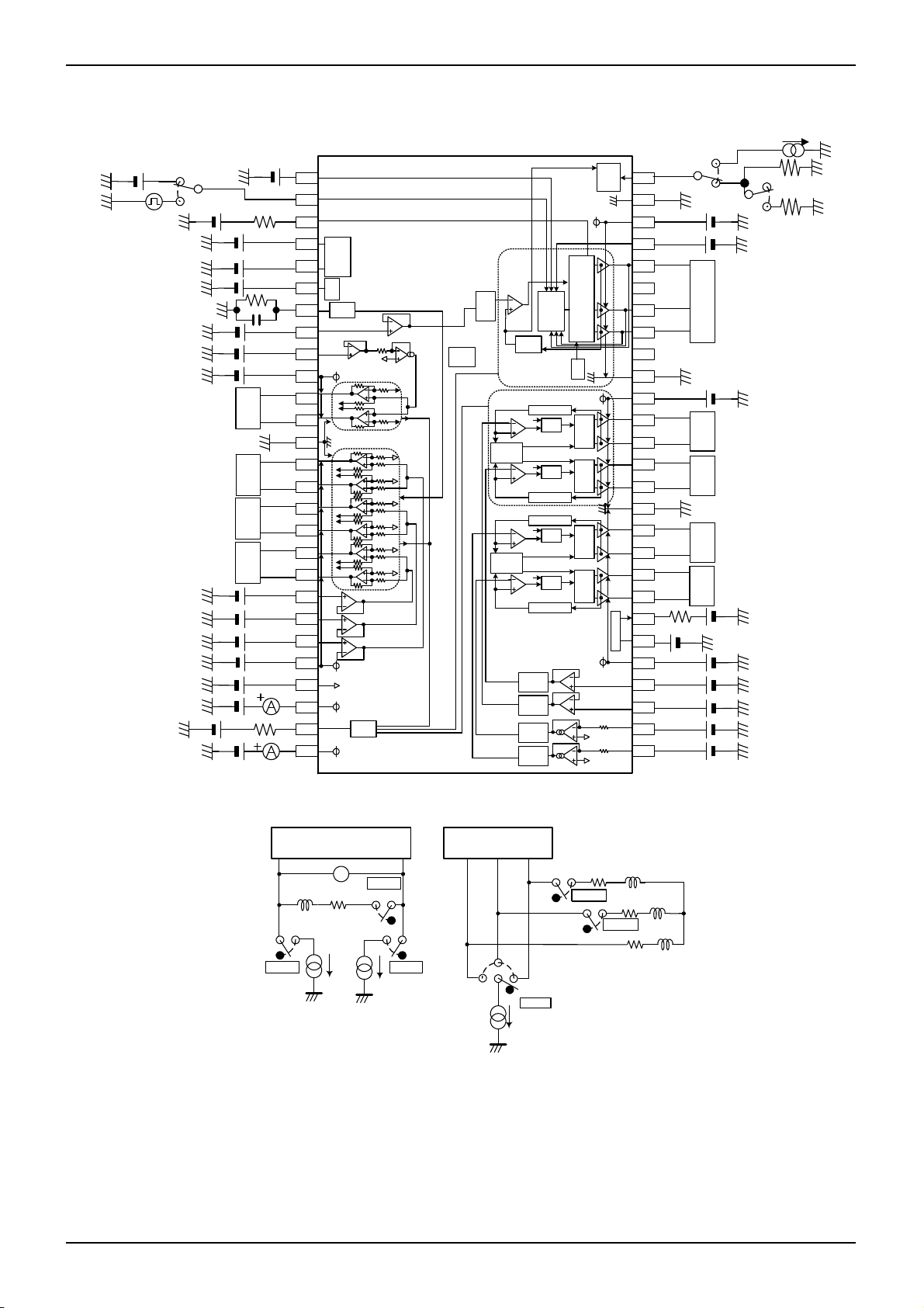
●Block diagram
Technical Note
C_OUT
C_COM
FG
CTL1
CTL2
LRPM
PRTLIM
SPIN
LDIN
LDVM
LDO+
LDO-
AGND
FCO+
FCO-
TLO+
TLO-
TKO+
TKO-
TKIN
TLIN
1
2
3
4
STBY
BRAKE
5
6
7
8
9
10
11
12
13
14
15
16
17
18
19
20
21
LRPM
PRTLIM
80kΩ
40kΩ
40kΩ
LDVM/2
80kΩ
160kΩ
160kΩ
AVM/2
160kΩ
160kΩ
160kΩ
160kΩ
160kΩ
AVM/2
160kΩ
160kΩ
160kΩ
160kΩ
AVM/2
160kΩ
CONTROL
SHIFT
40kΩ
80kΩ
80kΩ
26.5kΩ
26.5kΩ
26.5kΩ
26.5kΩ
26.5kΩ
26.5kΩ
26.5kΩ
26.5kΩ
26.5kΩ
26.5kΩ
26.5kΩ
26.5kΩ
LEVEL
×2
T.S.D
CURR.
LIMIT
CURR.
LIMIT
CURR.
FEED
CURR.FEED
OSC
OSC
CURR.FEED
CURR.FEED
OSC
OSC
CURR.FEED
BEMF
DETECTER
FFFF
FFFF
CURR.
Logic
OSC
PRE
Logic
PRE
Logic
PRE
Logic
PRE
Logic
54
LIMIT
SPLIM
53
GND
52
SPVM
51
COM
50
W
49
N.C.
48
V
47
U
46
N.C.
45
SPGND
44
SLVM
43
SLO2-
42
SLO2+
41
SLO1-
40
SLO1+
39
SL/SAGND
38
SAO2-
37
SAO2+
36
SAO1-
35
SAO1+
34
SLDETOUT
FCIN
AVM
VC
VCC
PRTFLG
DVCC
22
23
24
25
26
27
PROTECT
LEVEL
SHIFT
LEVEL
SHIFT
LEVEL
SHIFT
LEVEL
SHIFT
62.6kΩ
62.6kΩ
DETECTER
33
SLDET
32
SAVM
31
SLIN1
30
SLIN2
29
SAIN1
28
SAIN2
www.rohm.com
© 2010 ROHM Co., Ltd. All rights reserved.
4/18
2010.06 - Rev.A
Page 5

BD7755RFV
●Pin description
No. Symbol Description No. Symbol Description
Technical Note
1 C_OUT
2 C_COM
3 FG Frequency generator output 30 SLIN2 Sled driver 2 input
4 CTL1 Driver logic control 1 input 31 SLIN1 Sled driver 1 input
5 CTL2 Driver logic control 2 input 32 SAVM SA driver power block power supply
6 LRPM Low rotation mode change terminal 33 SLDET Sled motor detection signal control input
7 PRTLIM
8 SPIN Spindle driver input 35 SAO1+ SA driver 1 positive output
9 LDIN Loading driver input 36 SAO1- SA driver 1 negative output
10 LDVM Loading driver block power supply 37 SAO2+ SA driver 2 positive output
11 LDO+ Loading driver positive output 38 SAO2- SA driver 2 negative output
12 LDO- Loading driver negative output 39 SL/SAGND
13 AGND BTL driver block GND 40 SLO1+ Sled driver 1 positive output
Smooth capacitor connection terminal
(output side)
Smooth capacitor connection terminal
(com side)
Adjustable resistor connection for
actuator protection
28 SAIN2 SA driver 2 input
29 SAIN1 SA driver 1 input
34 SLDETOUT Sled motor detection signal output
Sled/SA driver block pre and power
ground
14 FCO+ Focus driver positive output 41 SLO1- Sled driver 1 negative output
15 FCO- Focus driver negative output 42 SLO2+ Sled driver 2 positive output
16 TLO+ Tilt driver positive output 43 SLO2- Sled driver 2 negative output
17 TLO- Tilt driver negative output 44 SLVM Sled motor driver power supply
18 TKO+ Tracking driver positive output 45 SPGND Spindle driver power ground
19 TKO- Tracking driver negative output 46 N.C. N.C.
20 TKIN Tracking driver input 47 U Spindle driver output U
21 TLIN Tilt driver input 48 V Spindle driver output V
22 FCIN Focus driver input 49 N.C. N.C.
23 AVM Actuator driver block power supply 50 W Spindle driver output W
24 VC Reference voltage input 51 COM Motor coil center point input
25 Vcc Pre block power supply 52 SPVM Spindle driver power supply
26 PRTFLG Protection flag output 53 GND Pre block GND
27 DVcc PWM block control power supply 54 SPLIM
*Positive/negative of the output terminals is determined in reference to those of the input terminals.
www.rohm.com
© 2010 ROHM Co., Ltd. All rights reserved.
5/18
Adjustable resistor connection for
spindle driver current limit
2010.06 - Rev.A
Page 6

BD7755RFV
●Equivalent-circuit diagram of the terminals
Three-phase motor driver output BEMF voltage detection input
Technical Note
51
52pin
10k
5k
1
2
5k 5k 10k
53pin
47
52
48 50
45
PWM driver output SLED1,2 PWM driver output SA1,2 BTL driver output FC,TK,TL
40
42
44
39
41
43
35
37
32
39
36
38
14
16
18
13
23
15
17
19
BTL driver output LD BTL driver input FC,TK,TL,LD PWM driver input SLED1,2
11
13
10
12
20
22
21
25pin
9
200Ω
53pin
30
31
27pin
200Ω
53pin
PWM driver input SA1,2 PWM driver input Spindle Spindle current limit input
52pin
54
53pin
28
29
27pin
53pin
62.6kΩ
27pin
8
200Ω
53pin
www.rohm.com
© 2010 ROHM Co., Ltd. All rights reserved.
6/18
2010.06 - Rev.A
Page 7

BD7755RFV
●Equivalent-circuit diagram of the terminals
PRTFLG, FG signal output SLDETOUT signal output SLED inner detection input
Technical Note
25pin
10kΩ
33
53pin
26
25pin
3
30Ω
27pin
30Ω
34
53pin
53pin
Actuator current limit input Control signal reference voltage input
25pin
25pin
7
53pin
10kΩ
5kΩ
24
53pin
62.6kΩ
200Ω
×2ch
10kΩ
×6ch
×2ch
10kΩ
50kΩ
50kΩ
Control signal input (CTL1) Control signal input (CTL2, LRPM)
25pin
25pin
50kΩ
4
50kΩ
53pin
180kΩ
20kΩ
53pin
270kΩ
5
20kΩ
53pin
150kΩ
50kΩ
50kΩ
150kΩ
150kΩ
50kΩ
50kΩ
150kΩ
25pin
6
53pin
53pin
120kΩ
100kΩ
www.rohm.com
© 2010 ROHM Co., Ltd. All rights reserved.
7/18
2010.06 - Rev.A
Page 8
BD7755RFV
●Test circuit
Technical Note
ISPLIM
CTL2
CTL1
LRPM
VSPIN
LDIN
LDVM
TKIN
TLIN
FCIN
AVM
VCC
COUT
100k
+ -
OUT
LD
+ -
OUT
FC
+ -
OUT
TL
+ -
OUT
TK
VC
100k
IQDVDVCC
IQVC
C_OUT
C_COM
CTL1
CTL2
LRPM
PRTLIM
SPIN
LDIN
LDVM
LDO+
LDO-
AGND
FCO+
FCO-
TLO+
TLO-
TKO+
TKO-
TKIN
TLIN
FCIN
AVM
VCC
PRTFLG
DVCC
1
2
3
FG
4
STBY
BRAKE
5
CONTROL
6
LRPM
PRTLIM
7
8
40kΩ
9
10
80kΩ
11
40kΩ
40kΩ
LDVM/2
12
80kΩ
13
160kΩ
14
160kΩ
AVM/2
160kΩ
15
160kΩ
160kΩ
16
160kΩ
160kΩ
AVM/2
17
160kΩ
160kΩ
18
160kΩ
160kΩ
AVM/2
19
160kΩ
×2
80kΩ
80kΩ
26.5kΩ
26.5kΩ
26.5kΩ
26.5kΩ
26.5kΩ
26.5kΩ
26.5kΩ
26.5kΩ
26.5kΩ
26.5kΩ
26.5kΩ
26.5kΩ
20
21
T.S.D
SHIFT
LEVEL
CURR.
FEED
CURR.FEED
OSC
CURR.
LIMIT
OSC
CURR.FEED
CURR.FEED
OSC
CURR.
LIMIT
OSC
CURR.FEED
Logic
BEMF
DETECTER
OSC
FFFF
PRE
Logic
PRE
Logic
FFFF
PRE
Logic
PRE
Logic
22
23
24
VC
25
26
PROTECT
27
LEVEL
SHIFT
LEVEL
SHIFT
LEVEL
SHIFT
LEVEL
SHIFT
62.6kΩ
62.6kΩ
54
LIMIT
CURR.
SPLIM
53
GND
52
SPVM
51
COM
50
W
49
N.C.
48
V
47
U
46
N.C.
45
SPGND
44
SLVM
43
SLO2-
42
SLO2+
41
SLO1-
40
SLO1+
39
SL/SAGND
38
SAO2-
37
SAO2+
36
SAO1-
35
SAO1+
34
SLDETOUT
33
DETECTER
SLDET
32
SAVM
31
SLIN1
30
SLIN2
29
SAIN1
28
SAIN2
100k
VSLDET
12
SPVM
COM
SP
OUT
U V W
SLVM
OUT
SLO2
+ -
OUT
SLO1
+ -
OUT
SAO2
+ -
OUT
SAO1
+ -
DVCC
SAVM
VSLIN1
VSLIN2
VSAIN1
VSAIN2
4.7kΩ
12
2kΩ
CCOM
CCOM
12
DVCC
DVCC
OUT+
OUT-A
V
Vo
RL
47µH
2
1
IL
SW-RL
2
2
IL
OUT-
1
1
SW-ILSW-IL
OUTSP
UWV
2-W
2-V
2-U
1
IL
SW-IL
RLSP
2
SW-RL
47µH
RLSP
RLSP
47µH
47µH
2
SW-RL
1
1
www.rohm.com
© 2010 ROHM Co., Ltd. All rights reserved.
8/18
2010.06 - Rev.A
Page 9

BD7755RFV
●Functional description
1-1. Driver logic control terminal 1and 2 (CTL1,2)
All drivers and spindle-drive braking modes can be switched on/off by inputting combinations of H-level signal (higher
than 2.5V and lower than 3.7V), L-level signal (lower than 0.5V) and HiZ signal (open) to these terminals.
・Driver ON/OFF logic table
mode
①
②
③
④
⑤
・Spindle braking mode table
mode
③
④
⑤
1-2.Spindle output mode
The spindle output changes as follows by the setting of LRPM and SPIN. (CTL1=H,CTL2=H or HiZ)
Rotation speed 0rpm 400rpm 4500rpm
1-3.Gain switching mode
CTL1 CTL2 SP SL(2ch) ACT(3ch) SA(2ch) LOADING
L, HiZ L, HiZ × × × × ×
H L × ○ × × ○
H HiZ ○ ○ ○ × ×
L, HiZ H ○ ○ ○ ○ × ○:ON
H H ○ ○ ○ ○ × ×:OFF
① Stand-by mode
The IC is brought into stand-by mode, and its power dissipation can be limited.
② Drivers muting
All output channels, except the loading and sled motor are muted and their outputs are turned off.
③ SA mute mode
The loading and SA driver are muted.
④⑤ Loading OFF mode
Only the loading driver is muted.
CTL1 CTL2 SPIN > VC SPIN < VC
H HiZ
L, HiZ H
H H
③⑤Reverse-rotation braking mode (spindle)
When SPIN < VC, all output are shorted to SPVM in 4500rpm (Typ.) or more, in less than
4500rpm (Typ.) the output become reverse-rotation braking mode.
Rotation speed is less than 140rpm when SPIN < VC, all the output are shorted to SPVM.
(However, the above-mentioned rotational speed is expressed in the case of 12pole motor.)
④ Short-circuit braking mode (spindle)
All the spindle driver outputs are shorted to SPVM when SPIN < VC.
Normal mode
LRPM=Low
⑥
LRPM mode
LRPM=High
* PWM frequency becomes 30kHz (Typ.) in LRPM mode.
The torque at SPIN<VC becomes a counter torque
⑥ Low rotation mode
Please make to low rotation mode (LRPM=HI) after it starts in normal mode (LRPM=L).
Spindle driver and actuator driver can be switched on/off by inputting combinations of H-level signal (higher than
2.5V and lower than 3.7V), L-level signal (lower than 0.5V) and HiZ signal (open) to LRPM terminal.
LRPM SP Gain ACT Gain (3ch)
L H gain (3.5A/V±0.82A/V) H gain (21.6dB±2dB)
HiZ L gain (0.7A/V±0.17A/V) H gain (21.6dB±2dB)
H L gain (0.7A/V±0.17A/V) L gain (15.6dB±2dB)
Forward-rotation mode
SPIN>VC 120°energizing 150°energizing
SPIN<VC 120°energizing 150°energizing Short brake
SPIN>VC 120°energizing
SPIN<VC (H,Hi-Z,Hi-Z)
Reverse-rotation braking mode (LRPM=L)
Short-circuit braking mode
Reverse-rotation braking mode (LRPM=L)
Technical Note
www.rohm.com
© 2010 ROHM Co., Ltd. All rights reserved.
9/18
2010.06 - Rev.A
Page 10

BD7755RFV
Technical Note
2. Output limit for spindle (SPLIM)
3. Torque command (SPIN) (SLIN1,2) (SAIN1,2)
The relation between (the torque command inputs) and (Iosp or Ioo) is expressed in the figure below: The gain is defined
by the inclination between two points. (Please exclude the dead zone from the input voltage when calculating Iop. )
Iop
Forward rotation
Input dead zone +
Input dead zone -
Gain
SPIN
SLIN1,2
VC
SAIN1,2
4. FG output (FG)
3FG output begins after 900°degrees in electric angle, after the start mode ends and the BEMF detection starts. When
the rotational speed becomes 24rpm (Max.) or less in case of brake, the FG output is fixed to high.
The above-mentioned rotation speed applies to the 12 pole motor.
5. Input/Output timing chart
BEMFU
BEMFV
BEMFW
SPIN
U
V
W
VC
SOURCE
MID
SINK
SOURCE
MID
SINK
SOURCE
MID
SINK
》
》
》
》
》
》
》
》》
》
》
》
》
》
www.rohm.com
© 2010 ROHM Co., Ltd. All rights reserved.
Ⅰ) Forward
-rotation mode
Ⅱ) Reverse-rotation
braking mode
10/18
Ⅲ) Short-circuit
braking mode
2010.06 - Rev.A
Page 11

BD7755RFV
Technical Note
6. Protect system 1
It is a function to mute the actuator outputs when the IC outputs the current more than the setting threshold value IPRTLIM
for 1.2sec because of the protection for the focus, the tracking, and the tilt coil. Outputs are muted similarly when the
output current of two or three CHs continuously exceed the threshold for 1.2sec.
It returns to normal operation by setting CTL2=L.
IPRTLIM =
A
RPRTLIM(Ω)
(A)
A = 8750
PRTFLG(OUTPUT) Actuator output (FCO/TKO/TLO)
H OFF
L active
MIN. TYP. MAX. Unit
Time until protection function operates 1.0 1.2 1.4 s
FCIN1 0
Current between
FCO outputs
Current between
TLO outputs
Current between
TKO outputs
CTL2
High
Low
FCIN1
0
0
0
reset
1.2sec mute 1.2sec mute
threshold current
threshold current
threshold current
Current between
FCO outputs
Current between
TLO outputs
Current between
TKO outputs
CTL2
High
Low
0
0
0
0
threshold current
threshold current
threshold current
7. Protect system 2
Function to protect against destruction of output terminal when output pin connects to GND or Vcc.
PRTFLG(OUTPUT) Spindle, Sled motor driver output
H OFF
L active
・Spindle, Sled motor
・When SINK side POWER transistor has been turned on, if the output voltage (SPVM/2&SLVM/2<TYP> or more) are
detected, the channel concerned will be turned off.
・When SOURCE side POWER transistor has been turned on, if the output voltage (SPVM/2&SLVM/2<TYP> or less ) are
detected, the channel concerned will be turned off.
www.rohm.com
© 2010 ROHM Co., Ltd. All rights reserved.
11/18
2010.06 - Rev.A
Page 12

BD7755RFV
8. Inner detection function
BEMF of the motor is monitored according to timing for the sled input signal to pass VC, and Sled is detected reaching the
inner. The judgment voltage of BEMF can be set according to the voltage input to the terminal SLDET. If BEMF below the
judgment voltage is detected twice continuously, it becomes SLDETOUT=L. The inner detection function can be turned off
with SLDET<0.5V. When the motor starts, the terminal SLDETOUT might become L because BEMF is unstable. Please
take measures such as installing the time of the mask when it starts for the detection prevention.
Judgment voltage Vbemf =2.1 × (SLDET - VC) + 0.49
SLIN1 SLIN2
VC
Motor
SLDETOUT
X
Instability
Stop
:Detection point
BEMF < Vbemt
:Detection point
BEMF > Vbemt
Technical Note
SLDET
9. PWM oscillation frequency
The PWM oscillation for driving the spindle and sled is free running.
The sled and SA oscillating frequency is 100kHz (Typ.)
The spindle oscillating frequency is 167kHz (Typ.)
10. Muting functions
a) VC-drop muting
When the voltage at VC terminal drops to a value lower than 0.7V (Typ.), the outputs of all the channels are turned off.
Set the VC terminal voltage higher than 1.0V.
b) Vcc-drop muting
When the voltage at DVcc terminal and Vcc terminal drop to lower than 3.85V (Typ.), the outputs of all the channels
are turned off.
c) Over voltage protection circuit
When the voltage at SPVM terminal exceed 14.1V (Typ.), only the spindle block output is turned off.
11. Thermal-shut down
Thermal-shutdown circuit (over-temperature protection circuit) is built in to prevent the IC from thermal breakdown. Use
the IC according to the thermal loss allowed in the package. In case the IC is left running over the allowed loss, the
junction temperature rises, and the thermal-shutdown circuit works at a junction temperature of 175℃(Typ.) (All other
channel outputs are turned off)
When the junction temperature drops to 150℃ (Typ.) the IC resumes operation.
www.rohm.com
© 2010 ROHM Co., Ltd. All rights reserved.
12/18
2010.06 - Rev.A
Page 13

BD7755RFV
●Notes for use
1. Absolute maximum ratings
We are careful enough for quality control about this IC. So, there is no problem under normal operation, excluding that it
exceeds the absolute maximum ratings. However, this IC might be destroyed when the absolute maximum ratings, such
as impressed voltages (Vcc, PVcc) or the operating temperature range(Topr), is exceeded, and whether the destruction is
short circuit mode or open circuit mode cannot be specified. Please take into consideration the physical countermeasures
for safety, such as fusing, if a particular mode that exceeds the absolute maximum rating is assumed.
2. Power supply line
Due to switching and EMI noise generated by magnetic components (inductors and motors), using electrolytic and ceramic
suppress filter capacitors(0.1μF) close to the IC power input terminals (Vcc and GND) is recommended. Please note: the
electrolytic capacitor value decreases at lower temperatures. Current rush might flow momentarily by the order of turning
on the power supply and the delay in IC with two or more power supplies. Note the capacity of the power supply coupling,
width and drawing the power supply and the GND pattern wiring.Please make the power supply lines (where large current
flow) wide enough to reduce the resistance of the power supply patterns, because the resistance of power supply pattern
might influence the usual operation (output dynamic range etc…).
3. GND line
The ground line is where the lowest potential and transient voltages are connected to the IC.
4. Thermal design
Do not exceed the power dissipation (Pd) of the package specification rating under actual operation, and please design
enough temperature margins.
5. Short circuit mode between terminals and wrong mounting
Do not mount the IC in the wrong direction and be careful about the reverse-connection of the power connector. Moreover,
this IC might be destroyed when the dust short the terminals between them or GND
6. Radiation
Strong electromagnetic radiation can cause operation failures.
7. ASO(Area of Safety Operation.)
Do not exceed the maximum ASO and the absolute maximum ratings of the output driver.
8. TSD(Thermal shut-down)
The TSD is activated when the junction temperature (Tj) reaches 175℃(with 25℃ hysteresis), and the output terminal is
switched to Hi-z. The TSD circuit aims to intercept IC from high temperature. The guarantee and protection of IC are not
purpose. Therefore, please do not use this IC after TSD circuit operates, nor use it for assumption that operates the TSD
circuit.
9. Inspection by the set circuit board
The stress might hang to IC by connecting the capacitor to the terminal with low impedance. Then, please discharge
electricity in each and all process. Moreover, in the inspection process, please turn off the power before mounting the IC,
and turn on after mounting the IC. In addition, please take into consideration the countermeasures for electrostatic
damage, such as giving the earth in assembly process, transportation or preservation.
Technical Note
www.rohm.com
© 2010 ROHM Co., Ltd. All rights reserved.
13/18
2010.06 - Rev.A
Page 14

BD7755RFV
Technical Note
10. Earth wiring pattern
This IC is a monolithic IC, and has P+ isolation and P substrate for the element separation. Therefore, a parasitic PN
junction is firmed in this P-layer and N-layer of each element. For instance, the resistor or the transistor is connected to the
terminal as shown in the figure below. When the GND voltage potential is greater than the voltage potential at Terminals A
or B, the PN junction operates as a parasitic diode. In addition, the parasitic NPN transistor is formed in said parasitic diode
and the N layer of surrounding elements close to said parasitic diode. These parasitic elements are formed in the IC
because of the voltage relation. The parasitic element operating causes the wrong operation and destruction. Therefore,
please be careful so as not to operate the parasitic elements by impressing to input terminals lower voltage than GND(P
substrate). Please do not apply the voltage to the input terminal when the power-supply voltage is not impressed. Moreover,
please impress each input terminal lower than the power-supply voltage or equal to the specified range in the guaranteed
voltage when the power-supply voltage is impressing.
Terminal-A
+
P
Parasitic
element
Resistor
P
P-Substrate
GND
Transistor(NPN)
GND
Terminal-B
Surrounding
elements
C
B
E
Parasitic
element
GND
Terminal-B
Terminal-A
+
P
Parasitic
element
CB
+
P
Parasitic
element
E
P
P-Substrate
GND
+
P
Simplified structure of IC
11. Earth wiring pattern
Use separate ground lines for control signals and high current power driver outputs. Because these high current outputs
that flows to the wire impedance changes the GND voltage for control signal. Therefore, each ground terminal of IC must
be connected at the one point on the set circuit board. As for GND of external parts, it is similar to the above-mentioned.
12. Reverse-rotation braking
In the case of reverse-rotation braking from high speed rotation, pay good attention to reverse electromotive force.
Furthermore, fully check the voltage to be applied to the output terminal and consider the revolutions applied to the
reverse-rotation brake.
13. About the capacitor between SPVM and SPGND
The capacitor between SPVM and SPGND absorbs the change in a steep voltage and the current because of the PWM
drive, as a result, there is a role to suppress the disorder of the SPVM voltage. However, the effect falls by the influence of
the wiring impedance etc, if the capacitor becomes far from IC. Please examine the capacitor between SPVM and SPGND
to arrange it near IC.
www.rohm.com
© 2010 ROHM Co., Ltd. All rights reserved.
14/18
2010.06 - Rev.A
Page 15
BD7755RFV
●Application circuit
,
1000pF
M
PRTFLG
C_OUT
C_COM
FG
CTL1
CTL2
LRPM
PRTLIM
SPIN
LDIN
LDVM
LDO+
LDO-
AGND
FCO+
FCO-
TLO+
TLO-
TKO+
TKO-
TKIN
TLIN
FCIN
AVM
VC
VCC
DVCC
Technical Note
1
2
3
4
STBY
5
BRAKE
CONTROL
6
LRPM
7
PRTLIM
8
9
10
11
12
13
14
15
16
17
18
19
20
21
22
23
24
25
26
27
80kΩ
40kΩ
40kΩ
LDVM/2
80kΩ
160kΩ
160kΩ
AVM/2
160kΩ
160kΩ
160kΩ
160kΩ
160kΩ
AVM/2
160kΩ
160kΩ
160kΩ
160kΩ
AVM/2
160kΩ
PROTECT
40kΩ
26.5kΩ
26.5kΩ
26.5kΩ
26.5kΩ
26.5kΩ
26.5kΩ
26.5kΩ
26.5kΩ
26.5kΩ
26.5kΩ
26.5kΩ
26.5kΩ
×2
80kΩ
80kΩ
T.S.D
SHIFT
LEVEL
CURR.
FEED
CURR.FEED
OSC
CURR.
LIMIT
OSC
CURR.FEED
CURR.FEED
OSC
CURR.
LIMIT
OSC
CURR.FEED
LEVEL
SHIFT
LEVEL
SHIFT
LEVEL
SHIFT
LEVEL
SHIFT
Logic
BEMF
DETECTER
OSC
FFFF
PRE
Logic
PRE
Logic
FFFF
PRE
Logic
PRE
Logic
62.6kΩ
62.6kΩ
LIMIT
CURR.
DETECTER
54
SPLIM
53
GND
52
SPVM
51
COM
50
W
49
N.C.
48
V
47
U
46
N.C.
45
SPGND
44
SLVM
43
SLO2-
42
SLO2+
41
SLO1-
SLO1+
40
39
SL/SAGND
38
SAO2-
37
SAO2+
36
SAO1-
35
SAO1+
34
SLDETOUT
33
SLDET
32
SAVM
31
SLIN1
30
SLIN2
29
SAIN1
28
SAIN2
1.5kΩ
STM
STM
www.rohm.com
© 2010 ROHM Co., Ltd. All rights reserved.
15/18
2010.06 - Rev.A
Page 16

BD7755RFV
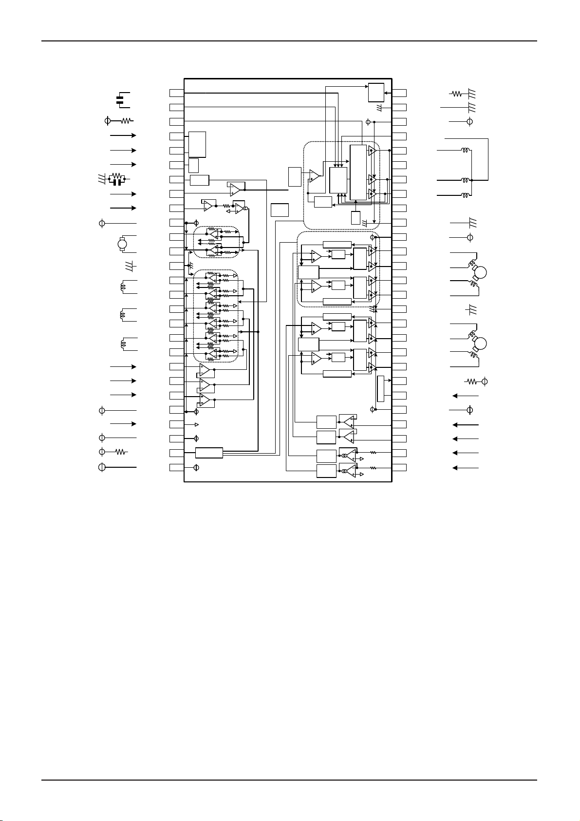
●Connecting wires of application board
Technical Note
www.rohm.com
© 2010 ROHM Co., Ltd. All rights reserved.
16/18
2010.06 - Rev.A
Page 17
BD7755RFV
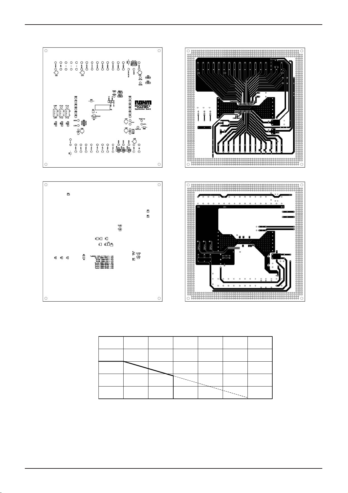
●Pattern drawing of application board
Technical Note
●Power dissipation reduction
2.0
1.5W
1.0
Power dissipation : Pd (W)
*70mm×70mm, t=1.6mm, occupied copper foil is less than 3%, glass epoxy mounting.
www.rohm.com
© 2010 ROHM Co., Ltd. All rights reserved.
25 50 75 100 125 1500
AMBIENT TEMPERATURE : Ta (℃)
17/18
2010.06 - Rev.A
Page 18

BD7755RFV
●Ordering part number
B D 7 7 5 5 R F V - E 2
Part No. Part No.
7755
HTSSOP-B54R
9.5±0.2
7.5±0.1
0.8
18.5±0.1
(MAX 18.85 include BURR)
(6.0)
54 28
1PIN MARK
+
6°
4°
−
4°
(5.0)
0.5±0.15
1.0±0.2
271
+0.05
0.17
-
0.03
S
Package
RFV: HTSSOP-B54R
<Tape and Reel information>
Embossed carrier tape (with dry pack)Tape
Quantity
Direction
of feed
1500pcs
E2
The direction is the 1pin of product is at the upper left when you hold
()
reel on the left hand and you pull out the tape on the right hand
Packaging and forming specification
E2: Embossed tape and reel
(HTSSOP-B54R)
Technical Note
1.0MAX
0.85±0.05
0.08±0.05
0.65
0.22
+0.05
-
0.04
0.08
0.08
S
M
(Unit : mm)
Reel
1pin
Order quantity needs to be multiple of the minimum quantity.
∗
Direction of feed
www.rohm.com
© 2010 ROHM Co., Ltd. All rights reserved.
18/18
2010.06 - Rev.A
Page 19

Notes
No copying or reproduction of this document, in part or in whole, is permitted without the
consent of ROHM Co.,Ltd.
The content specied herein is subject to change for improvement without notice.
The content specied herein is for the purpose of introducing ROHM's products (hereinafter
"Products"). If you wish to use any such Product, please be sure to refer to the specications,
which can be obtained from ROHM upon request.
Examples of application circuits, circuit constants and any other information contained herein
illustrate the standard usage and operations of the Products. The peripheral conditions must
be taken into account when designing circuits for mass production.
Great care was taken in ensuring the accuracy of the information specied in this document.
However, should you incur any damage arising from any inaccuracy or misprint of such
information, ROHM shall bear no responsibility for such damage.
The technical information specied herein is intended only to show the typical functions of and
examples of application circuits for the Products. ROHM does not grant you, explicitly or
implicitly, any license to use or exercise intellectual property or other rights held by ROHM and
other parties. ROHM shall bear no responsibility whatsoever for any dispute arising from the
use of such technical information.
Notice
The Products specied in this document are intended to be used with general-use electronic
equipment or devices (such as audio visual equipment, ofce-automation equipment, communication devices, electronic appliances and amusement devices).
The Products specied in this document are not designed to be radiation tolerant.
While ROHM always makes efforts to enhance the quality and reliability of its Products, a
Product may fail or malfunction for a variety of reasons.
Please be sure to implement in your equipment using the Products safety measures to guard
against the possibility of physical injury, re or any other damage caused in the event of the
failure of any Product, such as derating, redundancy, re control and fail-safe designs. ROHM
shall bear no responsibility whatsoever for your use of any Product outside of the prescribed
scope or not in accordance with the instruction manual.
The Products are not designed or manufactured to be used with any equipment, device or
system which requires an extremely high level of reliability the failure or malfunction of which
may result in a direct threat to human life or create a risk of human injury (such as a medical
instrument, transportation equipment, aerospace machinery, nuclear-reactor controller, fuelcontroller or other safety device). ROHM shall bear no responsibility in any way for use of any
of the Products for the above special purposes. If a Product is intended to be used for any
such special purpose, please contact a ROHM sales representative before purchasing.
If you intend to export or ship overseas any Product or technology specied herein that may
be controlled under the Foreign Exchange and the Foreign Trade Law, you will be required to
obtain a license or permit under the Law.
Thank you for your accessing to ROHM product informations.
More detail product informations and catalogs are available, please contact us.
ROHM Customer Support System
www.rohm.com
© 2010 ROHM Co., Ltd. All rights reserved.
http://www.rohm.com/contact/
R1010
A
 Loading...