


ROHM’s Selection Operational Amplifier/Comparator Series
High Voltage Operation CMOS
Operational Amplifiers:Input/Output Full Swing
BD7561G,BD7561SG,BD7541G,BD7541SG,
BD7562F/FVM,BD7562SF/FVM,BD7542F/FVM,BD7542SF/FVM
●Description
High voltage operable CMOS Op- A m p BD7561/BD7541 family and BD7562/BD7542 family Integrate one or two independent
input-output fullswing Op-amps and phase compesation capacitorson a single chip.
Especially, characteristics are wide operati ng vol t age range o f +5[V]~+14.5[V](single power supply),low supply current and little
input bias current.
High speed
Low power
●Features
1) Wide operating supply voltage(+5[V]~+14.5[V])
2) +5[V]~+14.5[V](single supply)
±2.5[V]~±7.25[V](split supply)
3) Input and Output full swing
4) Internal phase compensation
5) High slew rate (BD7561 family,
BD7562 family)
6) Low supply current (BD7541 family, BD7542 family)
7) High large signal voltage gain
8) Internal ESD protection
Human body model (HBM) ±4000[V](Typ.)
9) Wide temperature range
-40[℃]~+85[℃] (BD7561G,BD7562
-40[℃]~+105[℃] (BD7561SG,BD7562S
●Pin Assignment
IN+
1
VDD
5
VSS
IN-
+
2
-
3
OUT
4
SSOP5
BD7561G
BD7561SG
BD7541G
BD7541SG
Single
Dual
Single
Dual
(BD7561SG:Operation guaranteed up t o +105
(BD7562SF/FVM:Operation guaranteed up to + 105
(BD7541SG
(BD7542SF/FVM
:
Operation guaranteed up to +
:
Operation guaranteed up to +
family, BD7541G,BD7542 family)
family, BD7541SG,BD7542S fa mily)
OUT1
IN1-
IN1+
VSS
SOP8 MSOP8
BD7562F
BD7562SF
BD7542F
BD7542SF
1
CH1
2
- +
3
4
CH2
+ -
℃)
℃)
105℃)
105℃)
8
7
6
5
BD7562FVM
BD7562SFVM
BD7542FVM
BD7542SFVM
No.09049EBT05
VDD
OUT2
IN2-
IN2+
www.rohm.com
© 2012 ROHM Co., Ltd. All rights reserved.
1/20
2012.09 - Rev.B

BD7561G,BD7561SG,BD7541G,BD7541SG,
BD7562F/FVM,BD7562SF/FVM, BD7542F/FVM,BD7542SF/FVM
●Absolute Maximum Ratings (Ta=25[℃])
Parameter Symbol
BD7561G,BD7562 F/FVM
BD7541G,BD7542 F/FVM
Rating
BD7561SG,BD7562S F/FVM
BD7541SG,BD7542S F/FVM
Technical Note
Unit
Supply Voltage VDD-VSS +15.5 V
Differential Input Voltage
(*1)
Vid VDD-VSS V
Input Common-mode Voltage Range Vicm (VSS-0.3)~(VDD+0.3) V
Operating Temperature Topr -40~+85 -40~+105 ℃
Storage Temperature Tstg -55~+125 ℃
Maximum Junction Temperature Tjmax +125 ℃
Note: Absolute maximum rating item indicates the condition which must not be exceeded.
Application of voltage in excess of absolute maximum rating or use out absoluted maximum rated temperature environment may cause deterioration of characteristics.
(*1) The voltage difference between inverting input and non-inverting input is the differential input voltage.
Then input terminal voltage is set to more then VSS.
●Electric Characteristics
○BD7561
Input Offset Voltage
Input Offset Current
Input Bias Current
Supply Current
High Level Output Voltage VOH 25℃ VDD-0.1 - - V RL=10[kΩ]
Low Level Output Voltage
family (Unless otherwise specified VDD=+12[V], VSS=0[V], Ta=25[℃])
Parameter Symbol
(*2)(*4)
Vio
(*2)
Iio 25℃ - 1 - pA -
(*2)
Ib 25℃ - 1 - pA -
T emperature
range
25℃ - 1 9
Full range - - 10
25℃ - 370 550
(*4)
IDD
Full range - - 600
25℃ - 440 650
Full range - - 700
VOL 25℃ - - VSS+0.1 V RL=10[kΩ]
Guaranteed limit
BD7561G,BD7561SG
Min. Typ. Max.
Unit Condition
mV VDD=5~14.5[V],VOUT=VDD/2
RL=∞ All Op-Amps
AV=0[dB],VDD=5[V],VIN=2.5[V]
μA
RL=∞ All Op-Amps
AV=0[dB],VDD=12[V],VIN=6.0[V]
Large Single Voltage Gain AV 25℃ 70 95 - dB RL=10[kΩ]
Input Common-mode Voltage Range Vicm 25℃ 0 - 12 V VDD-VSS=12[V]
Common-mode Rejection Ratio CMRR 25℃ 45 60 - dB Power Supply Rejection Ratio PSRR 25℃ 60 80 - dB Output Source Current
Output Sink Current
(*3)
IOH 25℃ 3 8 - mA VDD-0.4[V]
(*3)
IOL 25℃ 4 14 - mA VSS+0.4[V]
Slew Rate SR 25℃ - 0.9 - V/μs CL=25[pF]
Gain Bandwidth Product FT 25℃ - 1.0 - MHz CL=25[pF], AV=40[dB]
Phase Margin θ 25℃ - 50° - - CL=25[pF], AV=40[dB]
Total Harmonic Distortion THD 25℃ - 0.05 - % VOUT=1[Vp-p],f=1[kHz]
(*2) Absolute value
(*3) Under the high temperature environment, consider the power dissipation of IC when selecting the output current.
When the terminal short circuits are continuously output, the output current is reduced to climb to the temperature inside IC.
(*4) Full range:BD7561:Ta=-40[℃]~+85[℃] BD7561S:Ta=-40[℃]~+105[℃]
www.rohm.com
© 2012 ROHM Co., Ltd. All rights reserved.
2/20
2012.09 - Rev.B

BD7561G,BD7561SG,BD7541G,BD7541SG,
(*5)
BD7562F/FVM,BD7562SF/FVM, BD7542F/FVM,BD7542SF/FVM
Technical Note
○BD7562 family (Unless otherwise specified VDD=+12[V], VSS=0[V], Ta=25[℃])
Guaranteed limit
Parameter Symbol
T emperature
range
BD7562F/FVM
BD7562SF/FVM
Unit Condition
Min. Typ. Max.
Input Offset Voltage
Input Offset Current
Input Bias Current
Supply Current
High Level Output Voltage VOH 25℃ VDD-0.1 - - V RL=10[kΩ]
Low Level Output Voltage
(*2)(*4)
Vio
(*2)
Iio 25℃ - 1 - pA -
(*2)
Ib 25℃ - 1 - pA -
(*4)
IDD
VOL 25℃ - - VSS+0.1 V RL=10[kΩ]
25℃ - 1 9
Full range - - 10
25℃ - 750 1300
Full range - - 1500
25℃ - 900 1400
Full range - - 1600
mV VDD=5~14.5[V],VOUT=VDD/2
RL=∞ All Op-Amps
AV=0[dB],VDD=5[V],VIN=2.5[V]
μA
RL=∞ All Op-Amps
AV=0[dB],VDD=12[V],VIN=6.0[V]
Large Single Voltage Gain AV 25℃ 70 95 - dB RL=10[kΩ]
Input Common-mode Voltage Range Vicm 25℃ 0 - 12 V VDD-VSS=12[V]
Common-mode Rejection Ratio CMRR 25℃ 45 60 - dB Power Supply Rejection Ratio PSRR 25℃ 60 80 - dB Output Source Current
Output Sink Current
(*3)
IOH 25℃ 3 8 - mA VDD-0.4[V]
(*3)
IOL 25℃ 4 14 - mA VSS+0.4[V]
Slew Rate SR 25℃ - 0.9 - V/μs CL=25[pF]
Gain Bandwidth Product FT 25℃ - 1.0 - MHz CL=25[pF], AV=40[dB]
Phase Margin θ 25℃ - 50° - - CL=25[pF], AV=40[dB]
Total Harmonic Distortion THD 25℃ - 0.05 - % VOUT=1[Vp-p],f=1[kHz]
(*2) Absolute value
(*3) Under the high temperature environment, consider the power dissipation of IC when selecting the output current.
When the terminal short circuits are continuously output, the output current is reduced to climb to the temperature inside IC.
(*4) Full range: BD7562:Ta=-40[℃]~+85[℃] BD7562S:Ta=-40[℃]~+105[℃]
○BD7541 family (Unless otherwise specified VDD=+12[V], VSS=0[V], Ta=25[℃])
Parameter Symbol
Input Offset Voltage
Input Offset Current
Input Bias Current
(*5)(*7)
Vio
(*5)
Iio 25℃ - 1 - pA -
T emperature
range
25℃ - 1 9
Full range - - 10
Ib 25℃ - 1 - pA -
25℃ - 170 300
Supply Current
(*7)
IDD
Full range - - 400
25℃ - 180 320
Full range - - 420
High Level Output Voltage VOH 25℃ VDD-0.1 - - V RL=10[kΩ]
Low Level Output Voltage
VOL 25℃ - - VSS+0.1 V RL=10[kΩ]
Guaranteed limit
BD7541G,BD7541SG
Min. Typ. Max.
Unit Condition
mV VDD=5~14.5[V],VOUT=VDD/2
RL=∞ All Op-Amps
AV=0[dB],VDD=5[V],VIN=2.5[V]
μA
RL=∞ All Op-Amps
AV=0[dB],VDD=12[V],VIN=6.0[V]
Large Single Voltage Gain AV 25℃ 70 95 - dB RL=10[kΩ]
Input Common-mode Volt age Range Vicm 25℃ 0 - 12 V VDD-VSS=12[V]
Common-mode Rejection Ratio CMRR 25℃ 45 60 - dB Power Supply Rejection Ratio PSRR 25℃ 60 80 - dB Output Source Current
Output Sink Current
(*6)
IOH 25℃ 2 4 - mA VDD-0.4[V]
(*6)
IOL 25℃ 3 7 - mA VSS+0.4[V]
Slew Rate SR 25℃ - 0.3 - V/μs CL=25[pF]
Gain Bandwidth Product FT 25℃ - 0.6 - MHz CL=25[pF], AV=40[dB]
Phase Margin θ 25℃ - 50° - - CL=25[pF], AV=40[dB]
Total Harmonic Distortion THD 25℃ - 1 9 % VOUT=1[Vp-p],f=1[kHz]
(*5) Absolute value
(*6) Under the high temperature environment, consider the power dissipation of IC when selecting the output current.
When the terminal short circuits are continuously output, the output current is reduced to climb to the temperature inside IC.
(*7) Full range:BD7541:Ta=-40[℃]~+85[℃] BD7541S:Ta=-40[℃]~+105[℃]
www.rohm.com
© 2012 ROHM Co., Ltd. All rights reserved.
3/20
2012.09 - Rev.B

BD7561G,BD7561SG,BD7541G,BD7541SG,
(*5)
BD7562F/FVM,BD7562SF/FVM, BD7542F/FVM,BD7542SF/FVM
Technical Note
○BD7542 family (Unless otherwise specified VDD=+12[V], VSS=0[V], Ta=25[℃])
Guaranteed limit
Parameter Symbol
T emperature
range
BD7542 F/FVM
BD7542S F/FVM
Unit Condition
Min. Typ. Max.
Input Offset Voltage
Input Offset Current
Input Bias Current
Supply Current
High Level Output Voltage VOH 25℃ VDD-0.1 - - V RL=10[kΩ]
Low Level Output Voltage
(*5)(*7)
Vio
(*5)
Iio 25℃ - 1 - pA -
(*7)
IDD
Ib 25℃ - 1 - pA -
VOL 25℃ - - VSS+0.1 V RL=10[kΩ]
25℃ - 1 9
Full range - - 10
25℃ - 340 650
Full range - - 850
25℃ - 400 780
Full range - - 900
mV VDD=5~14.5[V],VOUT=VDD/2
RL=∞ All Op-Amps
AV=0[dB],VDD=5[V],VIN=2.5[V]
μA
RL=∞ All Op-Amps
AV=0[dB],VDD=12[V],VIN=6.0[V]
Large Single Voltage Gain AV 25℃ 70 95 - dB RL=10[kΩ]
Input Common-mode Volt age Range Vicm 25℃ 0 - 12 V VDD-VSS=12[V]
Common-mode Rejection Ratio CMRR 25℃ 45 60 - dB Power Supply Rejection Ratio PSRR 25℃ 60 80 - dB Output Source Current
Output Sink Current
(*6)
IOH 25℃ 2 4 - mA VDD-0.4[V]
(*6)
IOL 25℃ 3 7 - mA VSS+0.4[V]
Slew Rate SR 25℃ - 0.3 - V/μs CL=25[pF]
Gain Bandwidth Product FT 25℃ - 0.6 - MHz CL=25[pF], AV=40[dB]
Phase Margin θ 25℃ - 50° - - CL=25[pF], AV=40[dB]
Total Harmonic Distortion THD 25℃ - 0.05 - % VOUT=1[Vp-p],f=1[kHz]
(*5) Absolute value
(*6) Under the high temperature environment, consider the power dissipation of IC when selecting the output current.
When the terminal short circuits are continuously output, the output current is reduced to climb to the temperature inside IC.
(*7) Full range:BD7542:Ta=-40[℃]~+85[℃] BD7542S:Ta=-40[℃]~+105[℃]
www.rohm.com
© 2012 ROHM Co., Ltd. All rights reserved.
4/20
2012.09 - Rev.B

BD7561G,BD7561SG,BD7541G,BD7541SG,
p
(
(
])
y
y
y
y
y
y
y
y
y
y
y
(
(
])
BD7562F/FVM,BD7562SF/FVM, BD7542F/FVM,BD7542SF/FVM
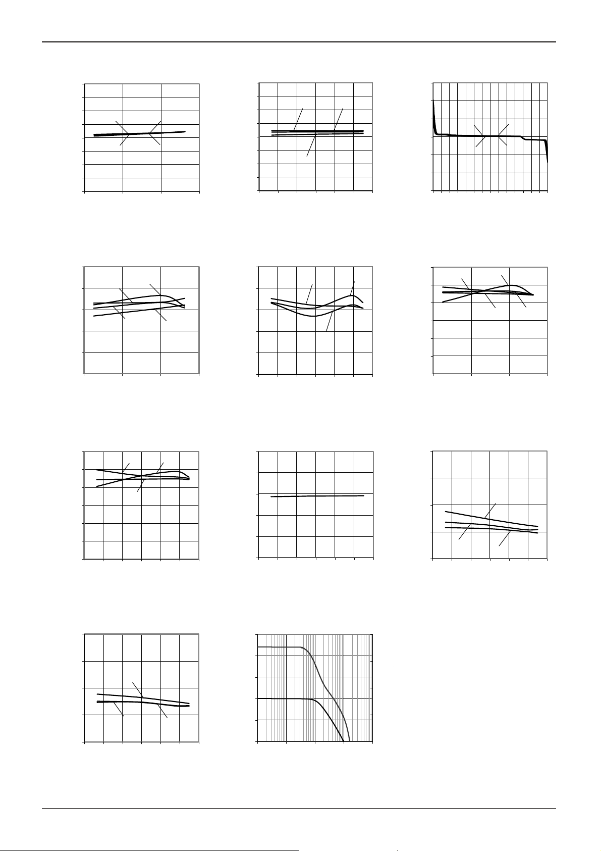
●Example of electrical characteristics
○BD7561 family
800
BD7561 family
800
BD7561 famil
800
Technical Note
BD7561 famil
600
BD7561G
400
200
POWER DISSIPATION [mW]
0
050100150
AMBIENT TEMPERATURE [°C]
Fig. 1 Fig. 2 Fig. 3
Derating Curve
800
600
14.5V
400
200
12V
5V
SUPPLY CURRENT [uA]
0
-60-300 306090120
AMBIENT TEMPERATURE [°C]
Fig. 4 Fig. 5 Fig. 6
Supply Current – Ambient Temperature
40
BD7561 famil
BD7561 famil
600
BD7561SG
400
200
POWER DISSIPATION [mW]
0
0 50 100 150
AMBIENT TEMPERATURE [°C]
Derating Curve
16
12
85℃
8
105℃
OUTPUT VOLTAGE HIGH [V]
4
481216
SUPPLY VOLTAGE [V]
BD7561 famil
-40℃
25℃
Output Voltage High – Supply Voltage
RL=10[kΩ
40
BD7561 famil
600
-40℃
25℃
400
200
SUPPLY CURRENT [uA]
SUPPLY CURRENT [μA]
105℃
85℃
0
481216
SUPPLY VOLTAGE [V]
Supply Current – Supply Voltage
16
12
8
5V
OUTPUT VOLTAGE HIGH [V]
4
-60-300 306090120
AMBIENT TEMPERATURE [°C]
BD7561 famil
14.5V
12V
Output Voltage High – Ambient Temperature
(RL=10[kΩ])
80
BD7561 famil
30
105℃
85℃
20
10
OUTPUT VOLTAGE LOW [mV]
0
Fig. 7 Fig. 8 Fig. 9
Output Voltage Low – Supply Voltage
15
12
25℃
-40℃
481216
SUPPLY VOLTAGE [V]
RL=10[kΩ])
BD7561 famil
14.5V
9
6
12V
3
5V
OUTPUT SOURCE CURRENT [mA]
0
-60-300 306090120
AMBIENT TEMPERATURE [°C]
Fig. 10 Fig. 11 Fig. 12
Output Source Current – Ambient
Tem
erature
(*)The above data is ability value of sample, it i s not guaranteed. BD7561:-40[ ℃]~+85[℃] BD7561S:-40[℃]~+105[℃]
VOUT=VDD-0.4[V])
30
14.5V
20
10
OUTPUT VOLTAGE LOW [mV]
0
5V
12V
-60 -30 0 30 60 90 120
AMBIENT TEMPERATURE [°C]
Output Voltage Low – Ambient Temperature
(RL=10[kΩ])
100
80
-40℃
BD7561 famil
60
25℃
40
20
OUTPUT SINK CURRENT [mA]
0
105℃
85℃
-10123
OUTPUT VOLTAGE [V]
Output Sink Current – Output Voltage
VDD=12[V
60
40
20
85℃
OUTPUT SOURCE CURRENT [mA]
0
8 9 10 11 12 13
OUTPUT VOLTAGE [V]
Output Source Current – Output Voltage
40
30
20
10
12V
OUTPUT SINK CURRENT [mA]
0
-60 -30 0 30 60 90 120
AMBIENT TEMPERATURE [°C]
Output Sink Current – Ambient Temperature
(VOUT=VDD-11.6[V])
-40℃
25℃
105℃
(VDD=12[V])
BD7561 famil
14.5V
5V
www.rohm.com
© 2012 ROHM Co., Ltd. All rights reserved.
5/20
2012.09 - Rev.B

BD7561G,BD7561SG,BD7541G,BD7541SG,
y
y
y
y
y
y
y
])
BD7562F/FVM,BD7562SF/FVM, BD7542F/FVM,BD7542SF/FVM
Technical Note
○BD7561 family
10.0
7.5
5.0
2.5
0.0
-2.5
-5.0
-7.5
INPUT OFFSET VOLTAGE [mV]
-10.0
Input Offset Voltage – Supply Voltage
160
140
120
100
80
60
LARGE SIGNAL VOLTAGE GAIN [dB]
120
100
-40℃
85℃
4 8 12 16
SUPPLY VOLTAGE [V]
Fig. 13 Fig. 14 Fig. 15
(Vicm=VDD, VOUT=VDD/2)
85℃
105℃
481216
SUPPLY VOLTAGE [V]
Fig. 16 Fig. 17 Fig. 18
Large Signal Voltage Gain
– Supply Voltage
5V
25℃
-40℃
BD7561 family
25℃
105℃
BD7561 famil
BD7561 famil
10.0
7.5
5.0
14.5V
2.5
0.0
INPUT OFFSET VOLTAGE [mV]
-2.5
-5.0
-7.5
-10.0
5V
-60 -30 0 30 60 90 120
AMBIENT TEMPERATURE [°C]
BD7561 family
12V
15
10
5
-40℃
0
-5
-10
INPUT OFFSET VOLTAGE [mV]
-15
-1 0 1 2 3 4 5 6 7 8 9 10111213
INPUT VOLTAGE [V]
Input Offset Voltage – Ambient Temperature
(Vicm=VDD, VOUT=VDD/2)
160
140
12V
120
100
5V
80
60
LARGE SIGNAL VOLTAGE GAIN [dB]
-60 -30 0 30 60 90 120
AMBIENT TEMPERATURE [°C]
BD7561 famil
14.5V
Input Offset Voltage – Input Voltage
120
25℃
100
80
60
[dB]
40
20
COMMON MODE RE J ECTION RATIO
0
481216
SUPPLY VOLTAGE [V]
Large Signal Voltage Gain
– Ambient Temperature
120
100
BD7561 famil
Common Mode Rejection Ratio
– Supply Voltage
4
3
80
60
14.5V
12V
40
20
COMMON MODE REJECTIO N RATIO [dB]
0
-60 -30 0 30 60 90 120
]
s
AMBIENT TEMPERATURE [°C]
Fig. 19 Fig. 20 Fig. 21
Common Mode Rejection Ratio
– Ambient Temperature
(VDD=12[V])
2.0
BD7561 famil
1.5
H-L [V/μ
14.5V
1.0
0.5
SLEW RATE
SLEW RATE H-L [V/us]
0.0
-60 -30 0 30 60 90 120
AMBIENT TEMPERATURE [°C]
Fig. 22 Fig. 23
12V
5V
Slew Rate H-L – Ambient
Temperature
80
60
40
20
POWER SUPPLY REJECTION RATIO [ dB]
0
-60 -30 0 30 60 90 120
AMBIENT TEMPERATURE [°C]
Power Supply Rejection Ratio
– Ambient Temperature
100
Phase
80
60
40
GAIN [dB]
Gain
20
0
1.E+00 1.E+02 1.E+04 1.E+06 1.E+08
FREQUENCY [Hz]
BD7561 famil
Gain - Frequency
200
150
100
50
0
2
1
SLEW RATE L-H [V/us]
12V
0
-60 -30 0 30 60 90 120
AMBIENT TEMPERATURE [°C]
Slew Rate L-H – Ambient Temperature
PHASE (deg)
PHASE[deg]
85℃
(VDD=12[V])
-40℃
85℃
(VDD=12[V
14.5V
5V
BD7561 famil
25℃
105℃
BD7561 family
105℃
BD7561 family
(*)The above data is ability value of sample, it is not guaranteed. BD7561:-40[℃]~+85[℃] BD7561S:-40[℃]~+105[℃]
www.rohm.com
© 2012 ROHM Co., Ltd. All rights reserved.
6/20
2012.09 - Rev.B

BD7561G,BD7561SG,BD7541G,BD7541SG,
y
y
y
y
y
y
y
p
(
])
(
(
)
BD7562F/FVM,BD7562SF/FVM, BD7542F/FVM,BD7542SF/FVM
Technical Note
○BD7562 family
800
BD7562 famil
800
BD7562 famil
1200
1000
600
400
BD7562F
BD7562FVM
200
POWER DISSIPATION [mW]
0
050100150
AMBIENT TEMPERATURE [°C]
Fig. 24 Fig. 25 Fig. 26
Derating Curve
1200
BD7562 family
14.5V
1000
800
600
400
SUPPLY CURRENT [uA]
200
SUPPLY CURRENT [μA]
0
-60-300 306090120
Fig. 27 Fig. 28 Fig. 29
Supply Current – Ambient Temperature
40
12V
AMBIENT TEMPERATURE [°C]
5V
BD7562 family
600
400
BD7562SF
BD7562SFVM
200
POWER DISSIPATION [mW]
0
050100150
AMBIENT TEMPERATURE [°C]
Derating Curve
16
12
85℃
8
OUTPUT VOLTAGE HIGH [V]
105℃
4
481216
SUPPLY VOLTAGE [V]
BD7562 famil
-40℃
25℃
Output Voltage High – Supply Voltage
RL=10[kΩ]
40
BD7562 family
800
600
400
SUPPLY CURRENT [uA]
200
SUPPLY CURRENT [μA]
0
481216
SUPPLY VOLTAGE [V]
Supply Current – Supply Voltage
16
12
8
OUTPUT VOLTAGE HIGH [V]
4
-60-300 306090120
AMBIENT TEMPERATURE [°C]
Output Voltage High – Ambient Temperature
80
BD7562 family
-40℃
25℃
85℃
105℃
BD7562 famil
14.5V
12V
5V
(RL=10[kΩ])
BD7562 famil
30
105℃
85℃
20
10
OUTPUT VOLTAGE LOW [mV]
25℃
-40℃
0
481216
Fig. 30 Fig. 31 Fig. 32
Output Voltage Low – Supply Voltage
15
12
SUPPLY VOLTAGE [V]
RL=10[kΩ])
BD7562 famil
14.5V
9
6
12V
3
OUTPUT SOURCE CURRENT [mA]
0
-60 -30 0 30 60 90 120
AMBIENT TEMPERATURE [°C]
Fig. 33 Fig. 34 Fig. 35
5V
Output Source Current – Ambient
Tem
erature
30
14.5V
20
10
OUTPUT VOLTAGE LOW [mV]
0
5V
12V
-60 -30 0 30 60 90 120
AMBIENT TEMPERATURE [°C]
Output Voltage Low – Ambient Temperature
(RL=10[kΩ])
100
BD7562 family
80
60
-40℃
40
20
OUTPUT SINK CURRENT [mA]
0
25℃
105℃
85℃
-1 0 1 2 3
OUTPUT VOLTAGE [V]
Output Sink Current – Output Voltage
VDD=12[V
60
40
20
OUTPUT SOURCE CU RRENT [mA]
0
85℃
105℃
8 9 10 11 12 13
OUTPUT VOLTAGE [V]
Output Source Current – Output Voltage
(VDD=12[V])
40
30
20
10
OUTPUT SINK CURRENT [mA]
0
12V
-60 -30 0 30 60 90 120
AMBIENT TEMPERATURE [°C]
Output Sink Current – Ambient Temperature
(VOUT=VDD-11.6[V])
-40℃
25℃
BD7562 famil
14.5V
5V
(*)The above data is ability value of sample, it i s not guaranteed. BD7562:-40[℃]~+85[℃] BD7562S:-40[℃]~+105[℃]
www.rohm.com
© 2012 ROHM Co., Ltd. All rights reserved.
7/20
2012.09 - Rev.B
BD7561G,BD7561SG,BD7541G,BD7541SG,
y
y
y
y
y
y
y
y
BD7562F/FVM,BD7562SF/FVM, BD7542F/FVM,BD7542SF/FVM
○BD7562 family
10.0
7.5
5.0
2.5
0.0
-2.5
-5.0
-7.5
INPUT OFFSET VO L T AG E [m V]
-10.0
Input Offset Voltage – Supply Voltage
160
140
120
100
80
-40℃
85℃
4 8 12 16
SUPPLY VOLTAGE [V]
Fig. 36 Fig. 37 Fig. 38
(Vicm=VDD, VOUT=VDD/2)
-40℃
105℃
85℃
BD7562 famil
25℃
105℃
BD7562 family
25℃
10.0
7.5
5.0
14.5V
2.5
0.0
-2.5
-5.0
-7.5
INPUT OFFSET VO L T AG E [m V]
-10.0
-60 -30 0 30 60 90 120
AMBIENT TEMPERATURE [°C]
Input Offset Voltage – Ambient Temperature
(Vicm=VDD, VOUT=VDD/2)
160
140
120
100
80
5V
14.5V
5V
BD7562 famil
12V
BD7562 famil
12V
Technical Note
15
10
5
-40℃
0
-5
85℃
-10
INPUT OFFSET VOLTAGE [mV]
-15
-1012345678910111213
INPUT VOLTAGE [V]
Input Offset Voltage – Input Voltage
(VDD=12[V])
120
100
80
60
40
20
85℃
25℃
105℃
-40℃
105℃
BD7562 family
BD7562 family
25℃
60
LARGE SIGNAL VOLTAGE G AIN [dB]
4 8 12 16
120
SUPPLY VOLTAGE [V]
Fig. 39 Fig. 40 Fig. 41
Large Signal Voltage Gain
– Supply Voltage
BD7562 famil
12V
5V
100
80
14.5V
60
40
20
COMMON MODE REJ ECTION RATIO [dB]
0
-60 -30 0 30 60 90 120
]
s
AMBIENT TEMPERATURE [°C]
Fig. 42 Fig. 43 Fig. 44
Common Mode Rejection Ratio
– Ambient Temperature
(VDD=12[V])
2.0
BD7562 famil
1.5
H-L [V/μ
1.0
0.5
SLEW RATE H-L [V/us]
SLEW RATE
0.0
-60 -30 0 30 60 90 120
Fig. 45 Fig. 46
14.5V
12V
5V
AMBIENT TEMPERATURE [°C]
Slew Rate H-L – Ambient
Temperature
(*)The above data is ability value of sample, it is not guaranteed. BD7562:-40[℃]~+85[℃] BD7562S:-40[℃]~+105[℃]
www.rohm.com
© 2012 ROHM Co., Ltd. All rights reserved.
60
LARGE SIGNAL VOLTAGE G AIN [dB]
-60 -30 0 30 60 90 120
AMBIENT TEMPERATURE [°C]
Large Signal Voltage Gain
– Ambient Temperature
200
160
120
80
40
0
POWER SUPPLY REJECT I ON RATIO [dB]
-60 -30 0 30 60 90 120
AMBIENT TEMPERATURE [°C]
BD7562 famil
Power Supply Rejection Ratio
– Ambient Temperature
100
Phase
80
60
40
GAIN [dB]
Gain
20
0
1.E+00 1.E+02 1.E+04 1.E+06 1.E+08
FREQUENCY [Hz]
BD7562 famil
Gain - Frequency
8/20
200
150
100
50
0
COMMON MODE REJECT IO N RAT IO [dB]
0
4 8 12 16
SUPPLY VOLTAGE [V]
Common Mode Rejection Ratio
– Supply Voltage
(VDD=12[V])
4
3
2
1
SLEW RATE L-H [V/us]
SLEW RATE L-H [V/μs]
12V
14.5V
5V
0
-60 -30 0 30 60 90 120
AMBIENT TEMPERATURE [°C]
Slew Rate L-H – Ambient Temperature
PHASE (deg)
PHASE[deg]
2012.09 - Rev.B
BD7562 famil

BD7561G,BD7561SG,BD7541G,BD7541SG,
y
y
y
y
y
y
y
y
y
y
y
p
(
])
(
(
])
(
)
BD7562F/FVM,BD7562SF/FVM, BD7542F/FVM,BD7542SF/FVM
Technical Note
○BD7541 family
800
600
400
200
POWER DISSIPATION [mW]
0
050100150
AMBIENT TEMPERATURE [°C]
Fig. 47 Fig. 48 Fig. 49
Derating Curve
400
300
200
100
SUPPLY CURRENT [uA]
SUPPLY CURRENT [μA]
0
Fig. 50 Fig. 51 Fig. 52
Supply Current – Ambient Temperature
80
12V
-60 -30 0 30 60 90 120
AMBIENT TEMPERATURE [°C]
BD7541G
14.5V
5V
BD7541 famil
BD7541 famil
BD7541 famil
800
BD7541 famil
600
400
BD7541SG
200
POWER DISSIPATION [mW]
0
0 50 100 150
AMBIENT TEMPERATURE [°C]
Derating Curve
16
12
85℃
8
OUTPUT VOLTAGE HIGH [V]
105℃
4
4 8 12 16
SUPPLY VOLTAGE [V]
BD7541 famil
-40℃
25℃
Output Voltage High – Supply Voltage
RL=10[kΩ
80
BD7541 famil
400
300
200
100
SUPPLY CURRENT [uA]
SUPPLY CURRENT [μA]
0
481216
SUPPLY VOLTAGE [V]
Supply Current – Supply Voltage
16
12
8
OUTPUT VOLTAGE HIGH [V]
4
-60 -30 0 30 60 90 120
AMBIENT TEMPERATURE [°C]
Output Voltage High – Ambient Temperature
40
-40℃
105℃
14.5V
12V
5V
RL=10[kΩ]
BD7541 famil
25℃
85℃
BD7541 famil
BD7541 famil
60
40
20
OUTPUT VOLTAGE LOW [mV]
0
4 8 12 16
105℃
5V
25℃
SUPPLY VOLTAGE [V]
Fig. 53 Fig. 54 Fig. 55
85℃
-40℃
Output Voltage Low – Supply Voltage
RL=10[kΩ])
10
BD7541 ファミリ
8
6
4
12V
14.5V
2
OUTPUT SOURCE CURRENT [mA]
0
5V
-60 -30 0 30 60 90 120
AMBIENT TEMPERATURE [°C]
Fig. 56 Fig. 57 Fig. 58
Output Source Current – Ambient
Tem
erature
60
14.5V
40
20
OUTPUT VOLTAGE LOW [mV]
12V
5V
0
-60 -30 0 30 60 90 120
AMBIENT TEMPERATURE [°C]
Output Voltage Low – Ambient Temperature
(RL=10[kΩ])
50
40
-40℃
BD7541 famil
30
25℃
20
10
OUTPUT SINK CURRENT [mA]
0
105℃
85℃
-10123
OUTPUT VOLTAGE [V]
Output Sink Current – Output Voltage
VDD=12[V
30
20
10
OUTPUT SOURCE CURRENT [mA]
0
85℃
105℃
8 9 10 11 12 13
OUTPUT VOLTAGE [V]
Output Source Current – Output Voltage
(VDD=12[V])
20
15
10
12V
5
OUTPUT SINK CURRENT [mA]
0
5V
-60 -30 0 30 60 90 120
AMBIENT TEMPERATURE [°C]
Output Sink Current – Ambient Temperature
(VOUT=VDD-11.6[V])
-40℃
25℃
BD7541 famil
14.5V
(*)The above data is ability value of sample, it i s not guaranteed. BD7541:-40[℃]~+85[℃] BD7541S:-40[℃]~+105[℃]
www.rohm.com
© 2012 ROHM Co., Ltd. All rights reserved.
9/20
2012.09 - Rev.B

BD7561G,BD7561SG,BD7541G,BD7541SG,
y
y
y
y
y
y
])
BD7562F/FVM,BD7562SF/FVM, BD7542F/FVM,BD7542SF/FVM
Technical Note
○BD7541 family
10.0
7.5
5.0
2.5
0.0
-2.5
-5.0
-7.5
INPUT OFFSET VOLTAGE [mV]
-10.0
Input Offset Voltage – Supply Voltage
160
140
120
100
80
-40℃
85℃
4 8 12 16
SUPPLY VOLTAGE [V]
Fig. 59 Fig. 60 Fig. 61
(Vicm=VDD, VOUT=VDD/2)
105℃
25℃
85℃
BD7541 famil
25℃
105℃
BD7541 family
-40℃
10.0
7.5
5.0
14.5V
2.5
0.0
INPUT OFFSET VOLTAGE [mV]
-2.5
-5.0
-7.5
-10.0
5V
-60 -30 0 30 60 90 120
AMBIENT TEMPERATURE [°C]
BD7541 famil
12V
15
10
5
-40℃
0
-5
85℃
-10
INPUT OFFSET VOLTAGE [mV]
-15
-1012345678910111213
INPUT VOLTAGE [V]
Input Offset Voltage – Ambient Temperature
(Vicm=VDD, VOUT=VDD/2)
160
140
120
100
80
5V
BD7541 famil
12V
14.5V
Input Offset Voltage – Input Voltage
(VDD=12[V])
120
-40℃
100
80
60
40
20
25℃
85℃
BD7541 famil
25℃
105℃
BD7541 famil
105℃
60
LARGE SIGNAL VOLTAGE GAIN [dB]
60
481216
Fig. 62 Fig. 63 Fig. 64
120
SUPPLY VOLTAGE [V]
Large Signal Voltage Gain
– Supply Voltage
BD7541 famil
100
80
14.5V
60
12V
5V
40
20
COMMON MODE REJECTIO N RATIO [dB]
0
-60 -30 0 30 60 90 120
]
s
H-L [V/μ
AMBIENT TEMPERATURE [°C]
Fig. 65 Fig. 66 Fig. 67
Common Mode Rejection Ratio
– Ambient Temperature
1.0
0.8
0.6
(VDD=12[V])
14.5V
BD7541 family BD7541 family
0.4
0.2
SLEW RATE H-L [V/us]
SLEW RATE
0.0
-60 -30 0 30 60 90 120
AMBIENT TEMPERATURE [°C]
Fig. 68 Fig. 69
Slew Rate H-L – Ambient Temperature
12V
(*)The above data is ability value of sample, it is not guaranteed. BD7541:-40[℃]~+85[℃] BD7541S:-40[℃]~+105[℃]
5V
LARGE SIGNAL VOLTAGE GA IN [dB]
-60 -30 0 30 60 90 120
AMBIENT TEMPERATURE [°C]
Large Signal Voltage Gain
– Ambient Temperature
200
160
120
80
40
0
POWER SUPPLY REJECTION RATIO [dB]
-60-300306090120
AMBIENT TEMPERATURE [°C]
BD7541 family
Power Supply Rejection Ratio
– Ambient Temperature
100
80
60
40
GAIN [dB]
20
0
1.E+00 1.E+02 1.E+04 1.E+06 1.E+08
Phase
Gain
FREQUENCY [Hz]
Gain - Frequency
200
150
100
50
0
COMMON MODE REJECTIO N RATIO [dB]
0
4 8 12 16
Common Mode Rejection Ratio
2.0
1.5
1.0
0.5
SLEW RATE L-H [V/us]
SLEW RATE L-H [V/μs]
0.0
-60-300 306090120
AMBIENT TEMPERATURE [°C]
Slew Rate L-H – Ambient Temperature
PHASE (deg)
PHASE[deg]
SUPPLY VOLTAGE [V]
– Supply Voltage
(VDD=12[V
14.5V
12V
5V
BD7541 family
www.rohm.com
© 2012 ROHM Co., Ltd. All rights reserved.
10/20
2012.09 - Rev.B

BD7561G,BD7561SG,BD7541G,BD7541SG,
y
y
y
y
y
y
y
(
])
(
(
])
BD7562F/FVM,BD7562SF/FVM, BD7542F/FVM,BD7542SF/FVM
Technical Note
○BD7542 family
800
600
400
200
POWER DISSIPATION [mW]
0
050100150
Fig. 70 Fig. 71 Fig. 72
800
600
BD7542F
BD7542FVM
AMBIENT TEMPERATURE [°C]
Derating Curve
14.5V
BD7542 famil
BD7542 family
800
600
400
BD7542SF
BD7542SFVM
200
POWER DISSIPATION [mW]
0
0 50 100 150
AMBIENT TEMPERATURE [°C]
Derating Curve
16
12
400
200
12V
5V
SUPPLY CURRENT [uA]
0
-60 - 30 0 30 60 90 120
AMBIENT TEMPERATURE [°C]
Fig. 73 Fig. 74 Fig. 75
Supply Current – Ambient Temperature
80
8
OUTPUT VOLTAGE HIGH [V]
4
Output Voltage High – Supply Voltage
80
85℃
105℃
4 8 12 16
SUPPLY VOLTAGE [V]
RL=10[kΩ
-40℃
BD7542 family
BD7542 famil
25℃
BD7542 family
800
600
400
200
SUPPLY CURRENT [uA]
0
4 8 12 16
SUPPLY VOLTAGE [V]
Supply Current – Supply Voltage
16
12
8
OUTPUT VOLTAGE HIGH [V]
4
-60 -30 0 30 60 90 120
AMBIENT TEMPERATURE [°C]
Output Voltage High – Ambient Temperature
40
BD7542 famil
-40℃
25℃
85℃
105℃
BD7542 famil
14.5V
12V
5V
(RL=10[kΩ])
BD7542 familyBD7542 famil
60
40
105℃
85℃
20
OUTPUT VOLTAGE LOW [m V]
25℃
0
481216
SUPPLY VOLTAGE [V]
Fig. 76 Fig. 77 Fig. 78
Output Voltage Low – Supply Voltage
10
-40℃
RL=10[kΩ])
BD7542 family
8
6
4
12V
14.5V
2
OUTPUT SOURCE CURRENT [mA]
0
-60 -30 0 30 60 90 120
Output Source Current – Ambient Temperature
AMBIENT TEMPERATURE [°C]
Fig. 79 Fig. 80 Fig. 81
5V
(VOUT=VDD-0.4[V])
60
14.5V
40
20
OUTPUT VOLTAGE LOW [mV]
12V
0
5V
-60 -30 0 30 60 90 120
AMBIENT TEMPERATURE [°C]
Output Voltage Low – Ambient Temperature
(RL=10[kΩ])
50
40
-40℃
BD7542 famil
30
20
25℃
10
OUTPUT SINK CURRENT [mA]
0
85℃
105℃
-10123
OUTPUT VOLTAGE [V]
Output Sink Current – Output Voltage
VDD=12[V
30
20
85℃
10
105℃
OUTPUT SOURCE CURRENT [mA]
0
8 9 10 11 12 13
OUTPUT VOLT AGE [V]
Output Source Current – Output Voltage
(VDD=12[V])
20
15
10
5
12V
OUTPUT SINK CURRENT [mA]
0
-60 -30 0 30 60 90 120
AMBIENT TEMPERATURE [°C]
Output Sink Current – Ambient Temperature
(VOUT=VDD-11.6[V])
(*)The above data is ability value of sample, it is not guaranteed. BD7561:-40[℃]~+85[℃] BD7561S:-40[℃]~+105[℃]
-40℃
25℃
BD7542 famil
14.5V
5V
www.rohm.com
© 2012 ROHM Co., Ltd. All rights reserved.
11/20
2012.09 - Rev.B

BD7561G,BD7561SG,BD7541G,BD7541SG,
y
y
y
y
y
(*)
]
[℃]
]
])
BD7562F/FVM,BD7562SF/FVM, BD7542F/FVM,BD7542SF/FVM
○BD7542 family
10.0
7.5
5.0
2.5
-40℃
0.0
-2.5
85℃
-5.0
-7.5
INPUT OFFSET VOLTAGE [mV]
-10.0
4 8 12 16
SUPPLY VOLTAGE [V]
Fig. 82 Fig. 83 Fig. 84
Input Offset Voltage – Supply Voltage
(Vicm=VDD, VOUT=VDD/2)
160
105℃
140
120
85℃
100
25℃
80
60
LARGE SIGNAL VOLTAGE GAIN [dB]
4 8 12 16
120
SUPPLY VOLTAGE [V]
Fig. 85 Fig. 86 Fig. 87
Large Signal Voltage Gain
– Supply Voltage
12V
100
80
14.5V
60
40
20
COMMON MODE REJECT IO N RA T IO [dB]
0
-60 -30 0 30 60 90 120
]
s
H-L [V/μ
AMBIENT TEMPERATURE [°C]
Fig. 88 Fig. 89 Fig. 90
Common Mode Rejection Ratio
– Ambient Temperature
(VDD=12[V])
1.0
0.8
0.6
14.5V
0.4
0.2
SLEW RATE H-L [V/us]
SLEW RATE
0.0
-60 -30 0 30 60 90 120
AMBIENT TEMPERATURE [°C]
Fig. 91 Fig. 92
Slew Rate H-L – Ambient
12V
Temperature
The above data is ability value of sample, it is not guaranteed. BD7561:-40[℃]~+85[℃
www.rohm.com
© 2012 ROHM Co., Ltd. All rights reserved.
BD7542 family
10.0
7.5
14.5V
25℃
5.0
2.5
0.0
105℃
-2.5
-5.0
-7.5
INPUT OFFSET VOLTAGE [mV]
-10.0
-60 -30 0 30 60 90 120
AMBIENT TEMPERATURE [°C]
Input Offset Voltage – Ambient Temperature
(Vicm=VDD, VOUT=VDD/2)
BD7542 famil
160
140
14.5V
120
-40℃
100
80
LARGE SIGNAL VOLTAGE GAIN [dB]
60
LARGE SIGNAL VOLTAGE GAIN [dB]
-60 -30 0 30 60 90 120
AMBIENT TEMPERATURE [°C]
Large Signal Voltage Gain
– Ambient Temperature
BD7542 famil
5V
200
160
120
80
40
POWER SUPPLY REJECTIO N RAT IO [dB]
0
-60 -30 0 30 60 90 120
AMBIENT TEMPERATURE [°C]
Power Supply Rejection Ratio
– Ambient Temperature
BD7542 famil
5V
100
Phase
80
60
40
GAIN [dB]
Gain
20
0
1.E+00 1.E+02 1.E+04 1.E+06 1.E+08
FREQUENCY [Hz]
Gain - Frequency
12/20
Technical Note
105℃
14.5V
5V
BD7542 family
25℃
105℃
BD7542 family
-40℃
BD7542 family
BD7542 family
12V
15
10
5
-40℃
0
5V
-5
85℃
-10
INPUT OFFSET VOLTAGE [mV]
-15
-1012345678910111213
INPUT VOLTAGE [V]
Input Offset Voltage – Input Voltage
(VDD=12[V])
BD7542 famil
12V
120
100
25℃
80
5V
60
85℃
40
20
COMMON MODE REJECT IO N RAT IO [dB]
0
4 8 12 16
SUPPLY VOLTAGE [V]
Common Mode Rejection Ratio
– Supply Voltage
BD7542 famil
2.0
]
s
1.5
L-H [V/μ
1.0
0.5
SLEW RATE L-H [V/us]
SLEW RATE
0.0
-60 -30 0 30 60 90 120
(VDD=12[V
12V
AMBIENT TEMPERATURE [°C]
Slew Rate L-H – Ambient Temperature
BD7542 family
200
150
100
50
0
PHASE[deg]
PHASE (deg)
BD7561S:-40
~+105[℃
2012.09 - Rev.B

BD7561G,BD7561SG,BD7541G,BD7541SG,
A
K
T
F
BD7562F/FVM,BD7562SF/FVM, BD7542F/FVM,BD7542SF/FVM
●Schematic diagram
Fig. 93. Schematic diagram
●Test circuit1 NULL method
VDD,VSS,EK,Vicm Unit : [V]
Parameter VF S1 S2 S3 VDD VSS EK Vicm Calculation
Technical Note
Input Offset Voltage VF1 ON ON OFF 12 0 -6 12 1
Large Signal Voltage Gain
Common-mode Rejection Ratio
(Input Common-mode Voltage Range)
Power Supply Rejection Ratio
VF2
VF3 -11.5
VF4
VF5 12
VF6
VF7 14.5
ON ON ON 12 0
ON ON OFF 12 0 -6
ON ON OFF
5
-0.5
6 2
0
0 -2.5 0 4
-Calculation-
1. Input Offset Voltage (Vio)
2. Large Signal Voltage Gain (Av)
3. Common-mode Rejection Ratio (CMRR)
Vio
CMRR
v
=
20Log
=
|VF1|
1+Rf/Rs
2×
20Log
=
[V]
(1+Rf/Rs)
|VF2-VF3|
1.8×
(1+Rf/Rs)
|VF4-VF5|
[dB]
[dB]
3.8×
4. Power Supply Rejection Ratio (PSRR)
PSRR
=
20Log
(1+Rf/Rs)
|VF6-VF7|
[dB]
0.1[μF]
SW1
VDD
0.015[μF]
Ri=1[MΩ]
Ri=1[MΩ]
SW2
0.015[μF]
DU
VSS
SW3
VRL50[kΩ]
RS=50[Ω]
RS=50[Ω] 1000[pF]
Vicm
Rf=50[kΩ]
500[kΩ]
E
Vo
500[kΩ]
RL
+
15[V]
NULL
-15[V]
0.01[μF]
V
Fig. 94. Test circuit 1 (one channel only)
3
www.rohm.com
© 2012 ROHM Co., Ltd. All rights reserved.
13/20
2012.09 - Rev.B
BD7561G,BD7561SG,BD7541G,BD7541SG,
2
8
L
2
L
o
BD7562F/FVM,BD7562SF/FVM, BD7542F/FVM,BD7542SF/FVM
Technical Note
●Test circuit2 switch condition
Unit : [V]
SW No.
SW 1 SW2 SW3 SW4 SW5 SW6 SW7 SW 8 SW 9 SW
10 SW11 SW12
Supply Current OFF OFF ON OFF ON OFF OFF OFF OFF OFF OFF OFF
Maximum Output Voltage RL=10 [kΩ] OFF ON OFF OFF ON OFF OFF ON OFF OFF ON OFF
Output Current OFF ON OFF OFF ON OFF OFF OFF OFF ON OFF OFF
Slew Rate OFF OFF ON OFF OFF OFF ON OFF ON OFF OFF ON
Maximum Frequency ON OFF OFF ON ON OFF OFF OFF ON OFF OFF ON
VIN
[V]
12[V]
SW3
SW4
R2 100[kΩ]
12[V
P-P
]
VDD=3[V]
SW1
1[kΩ]
SW
R1
SW5 SW6 SW7
VIN-
VIN+
-
+
GND
SW9SW10SW11SW
C
R
V
SW1
Fig. 95.. Test circuit2
0[V]
Input waveform
入力波形
VOUT
[V]
SR= ΔV / Δt
12[V]
Δt
0[V]
Output waveform
出力波形
Fig. 96.. Slew rate input output wave
●Test circuit3 Channel separation
R2=100[kΩ]
R2=100[kΩ]
R1=1[kΩ]
VDD
R1=1[kΩ]
VDD
VOUT1
VIN
R1//R2
VSS
V
=1[Vrms]
R1//R2
VSS
V
VOUT2
CS=20Log
100×VOUT1
VOUT2
Fig. 97.. Test circuit3
t
ΔV
t
www.rohm.com
© 2012 ROHM Co., Ltd. All rights reserved.
14/20
2012.09 - Rev.B

BD7561G,BD7561SG,BD7541G,BD7541SG,
BD7562F/FVM,BD7562SF/FVM, BD7542F/FVM,BD7542SF/FVM
●Description of electrical characteristics
Described here are the terms of electric characteristics used in this technical note. Items and symbols used are also shown.
Note that item name and symbol and their meaning may differ from those on another manufacture’s document or general document.
1. Absolute maximum ratings
Absolute maximum rating item indicates the condition which must not be exce eded. Application of voltage in excess of absolute
maximum rating or use out of absolute maximum rated temperature environment may cause deterioration of characteristics.
1.1 Power supply voltage (VDD/VSS)
Indicates the maximum voltage that can be applied between the positive power supply terminal and negative power supply
terminalwithout deterioration or destruction of characteristics of internal circuit.
1.2 Differential input voltage (Vid)
Indicates the maximum voltage that can be applied between non-inverting terminal and inverting terminal without
deterioration and destruction of characteristics of IC.
1.3 Input common-mode voltage range (Vicm)
Indicates the maximum voltage that can be applied to non-inverting terminal and inverting terminal without deterioration or
destruction of characteristics. Input common-mode voltage range of the maximum ratings not assure normal operation of
IC. When normal Operation of IC is desired, the input common-mode voltage of characteristics item must be followed.
1.4 Power dissipation (Pd)
Indicates the power that can be consumed by specified mounte d board at the ambient temperature 25℃( normal temperature).
As for package product, Pd is determined by the temperature that can be permitted by IC chip in the package(maximum
junction temperature)and thermal resistance of the package.
2. Electrical characteristics item
2.1 Input offset voltage (Vio)
Indicates the voltage difference between non-inverting terminal and inverting terminal. It can be translated into the input
voltage difference required for setting the output voltage at 0 [V].
2.2 Input offset current (Iio)
Indicates the difference of input bias current between non-inverting terminal and inverting terminal.
2.3 Input bias current (Ib)
Indicates the current that flows into or out of the input terminal. It is defined by the average of input bias current at
non-inverting terminal and input bias current at inverting terminal.
2.4 Circuit current (ICC)
Indicates the IC current that flows under specified conditions and no-load steady status.
2.5 High level output voltage / Low level output voltage(VOH/VOL)
Indicates the voltage range that can be output by the IC under specified load condition. It is typically divided into high-level
output voltage and low-level output voltage. High-level output voltage indicates the upper limit of output voltage. Low-level
output voltage indicates the lower limit.
2.6 Large signal voltage gain (AV)
Indicates the amplifying rate (gain) of output voltage against the voltage difference between non-inverting terminal and
inverting terminal.It is normally the amplifying rate (gain) with reference to DC voltage.
Av = (Output voltage fluctuation) / (Input offset fluctuation)
2.7 Input common-mode voltage range (Vicm)
Indicates the input voltage range where IC operates normally.
2.8 Common-mode rejection ratio (CMRR)
Indicates the ratio of fluctuation of input offset voltage when in-phase input voltage is changed. It is normally the fluctuation of DC.
CMRR =(Change of Input common-mode voltage)/(Input offset fluctuation)
2.9 Power supply rejection ratio (PSRR)
Indicates the ratio of fluctuation of input offset voltage when supply voltage is changed. It is normally the fluctuation of DC.
PSRR=(Change of power supply voltage)/(Input offset fluctuation)
2.10 Ch
annel separation(CS)
Indicates the fluctuation of input offset voltage or that of output voltage with reference to the change of output voltage of
driven channel.
Technical Note
www.rohm.com
© 2012 ROHM Co., Ltd. All rights reserved.
15/20
2012.09 - Rev.B

BD7561G,BD7561SG,BD7541G,BD7541SG,
BD7562F/FVM,BD7562SF/FVM, BD7542F/FVM,BD7542SF/FVM
Technical Note
2.11 Slew rate (SR)
Indicates the time fluctuation ratio of voltage output when step input signal is applied.
2.12 Unity gain frequency (ft)
Indicates a frequency where the voltage gain of Op-Amp is 1.
2.13 Total harmonic distortion + Noise (THD+N)
Indicates the fluctuation of input offset voltage or that of output voltage with reference to the change of output voltage
of driven channel.
2.14 Input referred noise voltage (Vn)
Indicates a noise voltage generated inside the operational amplifier equivalent by ideal voltage source connected in series
with input terminal.
●Derating curve
Power dissipation (total loss) indicates the power that can be consumed by IC at Ta=25℃(normal temperature).
IC is heatedwhen it consumed power, and the temperature of IC ship becomes higher than ambient temperature.
The temperature that can be accepted by IC chip depends on circuit configuration, manufacturing process, and consumable
power is limited. Power dissipation is determined by the temperature allowed in IC chip (maximum junction temperature) and
thermal resistance of pa ckage (heat di ssip a tion cap abi lity ).
The maximum junction temperature is typically equal to the maximum value in the storage package (heat dissipation capability).
The maximum junction temperature is typically equal to the maximum value in the storage temperatur e range.
Heat generated by consumed power of IC radiates from the mold resin or lead frame of the package.
The parameter which indicates this heat dissip ation cap ability (hardness of heat release) is calle d thermal resistance, represented
by the symbol θj-a[℃/W]. The temperature of IC inside the package can be estimated by this thermal resistance.
Fig.98 (a) shows the model of thermal resistance of the package. Thermal resistance θja, ambient temperature Ta, junction
temperature Tj, and power dissipation Pd can be calculated by the equation below :
θja = (Tj-Ta) / Pd [℃/W] ・・・・・ (Ⅰ)
Derating curve in Fig.98 (b) indicates power that can be consumed by IC with reference to ambient temperature.
Power that can be consumed by IC begins to attenuate at certain ambient temperature. This gradient iis determined by
thermal resistance θja.
Thermal resistance θja depends on chip size, power consumption, package, ambient temperature, package condition, wind
velocity, etc even when the same of package is used.
Thermal reduction curve indicates a reference value measured at a specified condition. Fig99(c)-(f) show a derating curve
for an example of BU7561family, BU7562family, 7541family, 7542family.
Power dissipation of LSI [W]
θja = (Tj-Ta) / Pd [℃/W]
Ta[℃]
Ambient temperature Ta [℃]
周囲温度
パッケージ表面温度
Package surface temperature [℃]
Ta[℃]
LSI
の消費電力
P2
P1
Pd(max)
[W]
θja1
θja2 <θja1
θja2
Tj(max)
0
25 125
Ambient temperature Ta [℃]
周囲温度
Ta[℃]
(b) Derating curve
75 15010050
BD7561/BD7541
Tj(max)
消費電力
Tj[℃]
P[W]
Fig. 98. Thermal resistance and derating
Chip surface temp er ature Tj [℃]
Power dissipation P [W]
(a) Thermal resistance
チップ表面温度
www.rohm.com
© 2012 ROHM Co., Ltd. All rights reserved.
16/20
2012.09 - Rev.B
BD7561G,BD7561SG,BD7541G,BD7541SG,
.
.
.
BD7562F/FVM,BD7562SF/FVM, BD7542F/FVM,BD7542SF/FVM
800
1000
600
400
540[mw
BD7561G(*8)
BD7541G(*8)
200
POWER DISSIPATION [mW] .
0
0 50 100 150
AMBIENT TEMPERATURE [℃]
85
(c) BD7561G
800
800
600
400
200
POWER DISSIP ATIO N [mW]
0
0 50 100 150
AMBIENT TEMPERATURE [℃]
(d) BD7562F/FVM BD7542F/FVM
1000
600
400
540[mw
BD7561SG(*8)
BD7541SG(*8)
200
POWER DISSIPATION [mW]
0
0 50 100 150
AMBIENT TEMPERATURE [℃]
(e) BD7561SG
105
800
600
400
200
POWER DISSIPATION [mW]
0
0 50 100 150
AMBIENT TEMPERATURE [℃]
(f) BD7562S F/FVM BD7542S F/FVM
(*8) (*9) (*10) Unit
5.4 6.2 4.8 [mW/℃]
When using the unit above Ta=25[℃], subtract the value above per degree[℃]. Permissible dissipation is the value
when FR4 glass epoxy board 70[mm]×70[mm]×1.6[mm] (cooper foil area below 3[%]) is mounted.
Fig. 99. Derating curve
620[mw]
480[mw]
620[mw]
480[mw]
BD7562F(*9
BD7542F(*9
BD7562FVM(*10)
BD7542FVM(*10)
85
BD7562SF(*9
BD7542SF(*9
BD7562SFVM(*10)
BD7542SFVM(*10)
105
Technical Note
www.rohm.com
© 2012 ROHM Co., Ltd. All rights reserved.
17/20
2012.09 - Rev.B

BD7561G,BD7561SG,BD7541G,BD7541SG,
BD7562F/FVM,BD7562SF/FVM, BD7542F/FVM,BD7542SF/FVM
●N0tes for use
1) Absolute maximum ratings
Absolute maximum ratings are the values which indicate the limits,within which the given voltage range can be safely
charged to the terminal.However, it does not guarantee the circuit operation.
2) Applied voltage to the input terminal
For normal circuit operation of voltage comparator, please input voltage for its input terminal within input common mode
voltage VDD+0.3[V].Then, regardless of power supply voltage,VSS-0.3[V] can be applied to inputterminals without
deterioration or destruction of its characteristics.
3) Operating power supply (split power supply/single power supply)
The voltage comparator operates if a given level of voltage is applied bet ween VDD and VSS. Therefore, the operational
amplifier can be operated under single power supply or split power supply.
4) Power dissipation (Pd)
If the IC is used under excessive power dissipation. An increase in the chip temperatur e will cause deterioration of the
radical characteristics of IC. For example, reduction of current capability. Take consideration of the effective power
dissipation andthermal design with a sufficient margin. Pd is reference to the provided power dissipation curve.
5) Short circuits between pins and incorrect mounting
Short circuits between pins and incorrect mounting when mounting the IC on a printed circuits board, take notice of the
direction and positioning of the IC.If IC is mounted erroneously, It may be dama ged. Also, when a foreign object is inserted
between output, between output and VDD terminal or VSS terminal which causes short circuit, the IC may be damaged.
6) Using under strong electromagnetic field
Be careful when using the IC under strong electromagnetic field because it may malfunction.
7) Usage of IC
When stress is applied to the IC through warp of the printed circuit board, The characteristics may fluctuate due to the
piezo effect. Be careful of the warp of the printed circuit board.
8) Testing IC on the set board
When testing IC on the set board, in cases where the capacitor is connected to the low impedance,make sure to discharge
per fabrication because there is a possibility that IC may be damaged by stress.
When removing IC from the set board, it is essential to cut supply voltage.As a countermeasure against the static
electricity, observe proper grounding during fabrication processand take due care when carrying and storage it.
9) The IC destruction caused by capacitive load
The transistors in circuits may be damaged when VDD terminal and VSS terminal is shorted with the charged output
terminal capacitor. When IC is used as a operational amplifier or as an application circuit,where oscillation is not activated
by an output capacitor, the output capacitor must be kept below 0.1[μF] in order to prevent the damage mentioned above.
10) Decupling capacitor
Insert the deculing capacitance between VDD and VSS, for stable operation of operational amplifier.
11) Latch up
Be careful of input vltage that exceed the VDD and VSS. When CMOS device have sometimes occur latch up operation.
And protect the IC from abnormaly noise.
Technical Note
www.rohm.com
© 2012 ROHM Co., Ltd. All rights reserved.
18/20
2012.09 - Rev.B

BD7561G,BD7561SG,BD7541G,BD7541SG,
BD7562F/FVM,BD7562SF/FVM, BD7542F/FVM,BD7542SF/FVM
●Ordering part number
B D 7 5 6 2 F V M - T R
Technical Note
ローム形名 品番
7561 , 7561S
7541 , 7541S
7562 , 7562S
7542 , 7542S
SOP8
6.2±0.3
1.5±0.1
5.0±0.2
(MAX 5.35 include BURR)
7
4.4±0.2
0.595
0.11
1.27
6
438251
0.42±0.1
+
6
°
4
°
−4°
0.3MIN
0.9±0.15
+0.1
0.17
-
0.05
S
(Unit : mm)
SSOP5
2.8±0.2
2.9±0.2
5
4
+0.2
−0.1
1.6
12
3
4
0.13
°
+
6
°
°
−4
0.2Min.
+0.05
−0.03
1.25Max.
1.1±0.05
0.05±0.05
0.95
+0.05
0.42
−0.04
0.1
(Unit : mm)
パッケージ
G: SSOP5
F: SOP8
FVM: MSOP8
<Tape and Reel information>
Embossed carrier tapeTape
Quantity
Direction
of feed
<Tape and Reel information>
Quantity
Direction
of feed
2500pcs
E2
The direction is the 1pin of product is at the upper left when you hold
()
reel on the left hand and you pull out the tape on the right hand
Reel
Embossed carrier tapeTape
3000pcs
TR
The direction is the 1pin of product is at the upper right when you hold
()
reel on the left hand and you pull out the tape on the right hand
Reel
Packaging and forming specification
E2: Embossed tape and reel
(SOP8)
TR: Embossed tape and reel
(SSOP5/MSOP8)
1pin
Order quantity needs to be multiple of the minimum quantity.
∗
1pin
Order quantity needs to be multiple of the minimum quantity.
∗
Direction of feed
Direction of feed
www.rohm.com
© 2012 ROHM Co., Ltd. All rights reserved.
19/20
2012.09 - Rev.B
BD7561G,BD7561SG,BD7541G,BD7541SG,
BD7562F/FVM,BD7562SF/FVM, BD7542F/FVM,BD7542SF/FVM
MSOP8
2.9±0.1
(MAX 3.25 include BURR)
4.0±0.2
0.475
0.9MAX
0.75±0.05
2.8±0.1
0.08±0.05
8
1
0.65
2
6
57
4
3
1PIN MARK
+0.05
0.22
–0.04
0.08 S
+
6°
4°
−4°
0.6±0.2
0.29±0.15
+0.05
0.145
–0.03
S
(Unit : mm)
<Tape and Reel information>
Quantity
Direction
of feed
Technical Note
Embossed carrier tapeTape
3000pcs
TR
The direction is the 1pin of product is at the upper right when you hold
()
reel on the left hand and you pull out the tape on the right hand
1pin
Direction of feed
Reel
Order quantity needs to be multiple of the minimum quantity.
∗
www.rohm.com
© 2012 ROHM Co., Ltd. All rights reserved.
20/20
2012.09 - Rev.B

Notes
No copying or reproduction of this document, in par t or in whole, is permitted without the
consent of ROHM Co.,Ltd.
The content specied herein is subject to change for improvement without notice.
The content specied herein is for the purpose of introducing ROHM's products (hereinafter
"Products"). If you wish to use any such Product, please be sure to refer to the specications,
which can be obtained from ROHM upon request.
Examples of application circuits, circuit constants and any other information contained herein
illustrate the standard usage and operations of the Products. The peripheral conditions must
be taken into account when designing circuits for mass production.
Great care was taken in ensuring the accuracy of the information specied in this document.
However, should you incur any damage arising from any inaccuracy or misprint of such
information, ROHM shall bear no responsibility for such damage.
The technical information specied herein is intended only to show the typical functions of and
examples of application circuits for the Products. ROHM does not grant you, explicitly or
implicitly, any license to use or exercise intellectual property or other rights held by ROHM and
other parties. ROHM shall bear no responsibility whatsoever for any dispute arising from the
use of such technical information.
The Products specied in this document are intended to be used with general-use electronic
equipment or devices (such as audio visual equipment, ofce-automation equipment, communication devices, electronic appliances and amusement devices).
The Products specied in this document are not designed to be radiation tolerant.
While ROHM always makes effor ts to enhance the quality and reliability of its Products, a
Product may fail or malfunction for a variety of reasons.
Please be sure to implement in your equipment using the Products safety measures to guard
against the possibility of physical injury, re or any other damage caused in the event of the
failure of any Product, such as derating, redundancy, re control and fail-safe designs. ROHM
shall bear no responsibility whatsoever for your use of any Product outside of the prescribed
scope or not in accordance with the instruction manual.
The Products are not designed or manufactured to be used with any equipment, device or
system which requires an extremely high level of reliability the failure or malfunction of which
may result in a direct threat to human life or create a risk of human injury (such as a medical
instrument, transportation equipment, aerospace machiner y, nuclear-reactor controller, fuelcontroller or other safety device). ROHM shall bear no responsibility in any way for use of any
of the Products for the above special purposes. If a Product is intended to be used for any
such special purpose, please contact a ROHM sales representative before purchasing.
If you intend to export or ship overseas any Product or technology specied herein that may
be controlled under the Foreign Exchange and the Foreign Trade Law, you will be required to
obtain a license or permit under the Law.
Notice
www.rohm.com
© 2012 ROHM Co., Ltd. All rights reserved.
Thank you for your accessing to ROHM product informations.
More detail product informations and catalogs are available, please contact us.
ROHM Customer Support System
http://www.rohm.com/contact/
R1120A
 Loading...