

Page 1
© 2017 ROHM Co., Ltd.
No. 60AP001E Rev.001
© 2018 ROHM Co., Ltd.
No. 61AN002E Rev.001
May.2018
2017.4
Application Note
2.7V to 5.5V
BD71837MWV
BUCK1 0.9V / 3.6A
i.MX 8M Quad
i.MX 8M QuadLite
i.MX 8M Dual
LDO1 3.3V / 10mA
Power Mux Switch
1.8V/3.3V / 150mA
LPDDR4 Memory
SD Card
USB /
Li-Ion Battery
BUCK2 1.0V / 4.0A
BUCK3 1.0V / 2.1A
BUCK4 1.0V / 1.0A
LDO2 0.9V / 10mA
LDO7 3.3V / 150mA
BUCK6 3.3V / 3.0A
LDO3 1.8V / 150mA
LDO5 1.8V / 300mA
BUCK7 1.8V / 1.5A
LDO4 0.9V / 250mA
LDO6 0.9V / 300mA
BUCK5 1.0V / 2.5A
BUCK8 1.1V / 3.0A
I2C (slave)
Power Mode
Control Signals
Power
Sequencing
Controller
Die temp
UVLO
32.768kHz Crystal Oscillator Driver
Interrupt
VR Fault
Power On Key
Detection
Power On Key
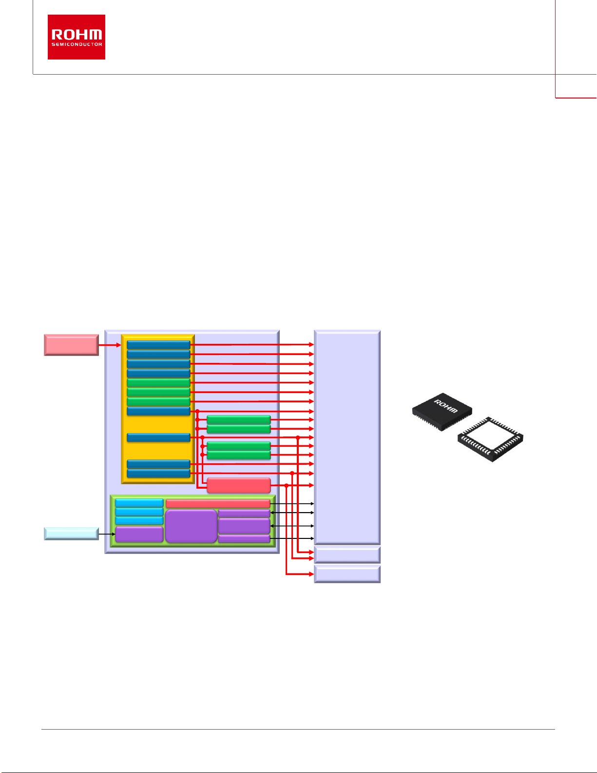
Figure 1.1 The system power map
Figure 1.2 The package image
Power Management IC designed for “NXP
®
i.MX 8M Quad”
BD71837MWV Platform Design Guide
1. Introduction
BD71837MWV is a Power Management Integrated Circuit (PMIC) available in 68-QFN package and dedicated to the application
powered by 5V input. PMIC includes eight Buck convertors, seven LDOs, one internal load switch and crystal oscillator driver for RTC
clock. These functions are designed to support the specific power requirements from NXP i.MX 8M platform to achieve the required
performance for cost-sensitive applications.
The below figure is the outline of the power map between PMIC and i.MX 8M SoC, showing that all voltage rails required by SoC are
satisfied.
“BD71837MWV Platform Design Guide” provides the guideline for designing PCB including recommendatio n for the PCB layer stack
up, the components placement and the PCB routings.
To reduce the risk that comes from PCB layout or parts placement, the guideline is strongly recommended to be applied to the PCB
design.
1/46
Page 2

Application Note
BD71837MWV Platform Design Guide
© 2018 ROHM Co., Ltd.
No. 61AN002E Rev.001
May.2018
1. Introduction ................................................................................................................................................................................ 1
2. Revision History ......................................................................................................................................................................... 4
3. Features ..................................................................................................................................................................................... 5
3.1. Terminologies ...................................................................................................................................................................... 5
3.2. Reference Documents ........................................................................................................................................................ 5
3.3. PMIC futures ....................................................................................................................................................................... 6
4. General Design Considerations ................................................................................................................................................. 7
4.1. Package Dimension of BD71837MWV ............................................................................................................................... 7
4.2. Pin Configuration ................................................................................................................................................................ 8
4.3. General Stack-up Recommendations ................................................................................................................................. 9
4.4. 6-layer Board Stack-up ....................................................................................................................................................... 9
4.5. Via Guidelines ................................................................................................................................................................... 10
4.6. Placement of PTHs underneath the exposed pad.............................................................................................................. 11
4.7. Outline for PCB layout ...................................................................................................................................................... 12
5. Platform Power Delivery Guidelines ......................................................................................................................................... 18
5.1. Platform Power Delivery ................................................................................................................................................... 18
5.2. General Layout Guideline ................................................................................................................................................. 20
5.2.1. Overall Component Placement .................................................................................................................................. 20
5.2.2. Large Current Loop .................................................................................................................................................... 21
5.2.3. Power GND ................................................................................................................................................................ 22
5.2.4. VSYS (Power supply for BD71837MWV analog circuit) ............................................................................................ 22
5.2.5. Other Signal Pattern Precautions .............................................................................................................................. 22
5.2.6. Feedback Sense Lines .............................................................................................................................................. 22
5.2.7. AGND layout .............................................................................................................................................................. 23
5.3. BUCK Convertors ............................................................................................................................................................. 24
5.3.1. BUCK1 (VDD_SoC) ................................................................................................................................................... 24
5.3.1.1. Schematic Example ............................................................................................................................................... 24
5.3.1.2. Schematic checklist ................................................................................................................................................ 24
5.3.1.3. Parts placement for each decoupling capacitor ...................................................................................................... 25
5.3.2. BUCK2 (VDD_ARM) .................................................................................................................................................. 25
5.3.2.1. Schematic Example ............................................................................................................................................... 25
5.3.2.2. Schematic checklist ................................................................................................................................................ 26
5.3.2.3. Layout Example ..................................................................................................................................................... 26
5.3.3. BUCK3 (VDD_GPU) .................................................................................................................................................. 27
5.3.3.1. Schematic Example ............................................................................................................................................... 27
5.3.3.2. Schematic Checklist ............................................................................................................................................... 27
5.3.3.3. Layout Example ..................................................................................................................................................... 28
5.3.4. BUCK4 (VDD_VPU) .................................................................................................................................................. 29
5.3.4.1. Schematic Example ............................................................................................................................................... 29
5.3.4.2. Schematic Checklist ............................................................................................................................................... 29
5.3.4.3. Layout Example ..................................................................................................................................................... 30
5.3.5. BUCK5 (VDD_DRAM) ............................................................................................................................................... 30
2/46
Page 3

Application Note
BD71837MWV Platform Design Guide
© 2018 ROHM Co., Ltd.
No. 61AN002E Rev.001
May.2018
5.3.5.1. Schematic Example ............................................................................................................................................... 30
5.3.5.2. Schematic Checklist ............................................................................................................................................... 31
5.3.5.3. Layout Example ..................................................................................................................................................... 32
5.3.6. BUCK6 (NVCC_3P3) ................................................................................................................................................. 32
5.3.6.1. Schematic Example ............................................................................................................................................... 32
5.3.6.2. Schematic Checklist ............................................................................................................................................... 33
5.3.6.3. Layout Example ..................................................................................................................................................... 33
5.3.7. BUCK7 (NVCC_1V8) ................................................................................................................................................. 34
5.3.7.1. Schematic Example ............................................................................................................................................... 34
5.3.7.2. Schematic Checklist ............................................................................................................................................... 34
5.3.7.3. Layout Example ..................................................................................................................................................... 35
5.3.8. BUCK8 (NVCC_DRAM) ............................................................................................................................................. 36
5.3.8.1. Schematic Example ............................................................................................................................................... 36
5.3.8.2. Schematic Checklist ............................................................................................................................................... 36
5.3.8.3. Layout Example ..................................................................................................................................................... 37
5.4. LDOs ................................................................................................................................................................................. 38
5.4.1. LDO1 (NVCC_SNVS) ................................................................................................................................................ 38
5.4.2. LDO2 (VDD_SNVS) ................................................................................................................................................... 38
5.4.3. LDO3 (VDDA_1P8/VDDA_DRAM) ............................................................................................................................ 38
5.4.4. LDO4 (VDDA_0P9) .................................................................................................................................................... 38
5.4.5. LDO5 (1P8_PHY) ...................................................................................................................................................... 38
5.4.6. LDO6 (0P9_PHY) ...................................................................................................................................................... 38
5.4.7. LDO7 (3P3_PHY) ...................................................................................................................................................... 38
5.4.8. Schematic Examples ................................................................................................................................................. 39
5.4.8.1. Schematic Checklist ............................................................................................................................................... 39
5.5. Load SW ........................................................................................................................................................................... 41
5.5.1. MUXSW (NVCC_SD2)............................................................................................................................................... 41
5.5.1.1. Schematic Examples .............................................................................................................................................. 41
5.5.1.2. Schematic Checklist ............................................................................................................................................... 41
5.6. Crystal Oscillator Driver .................................................................................................................................................... 42
5.6.1. XIN / XOUT / C32K_OUT .......................................................................................................................................... 42
5.6.1.1. Schematic Examples .............................................................................................................................................. 42
5.6.1.2. Schematic Checklist ............................................................................................................................................... 42
5.6.1.3. Layout Example ..................................................................................................................................................... 43
5.7. Interfaces .......................................................................................................................................................................... 44
5.7.1. I2C ................................................................................................ ............................................................................. 44
5.7.2. System Control – Reset, Power, and Control Signals ................................................................................................ 45
5.7.3. MISC .......................................................................................................................................................................... 46
3/46
Page 4

Application Note
BD71837MWV Platform Design Guide
© 2018 ROHM Co., Ltd.
No. 61AN002E Rev.001
May.2018
Revision Number
Description
Revision Date
001
Initial release
May. 1st, 2018
2. Revision History
Table 2.1 Revision History
4/46
Page 5
Application Note
BD71837MWV Platform Design Guide
© 2018 ROHM Co., Ltd.
No. 61AN002E Rev.001
May.2018
Term
Definition
BOM
Bill Of Materials
PMIC
Power Management Integrated Circuit
FET
Field Effect Transistor
I2C
Inter-Integrated Circuit
IRQ
Interrupt ReQuest
LDO
Low Drop-Out Regulator
OCP
Over Current Protection
OVP
Over Voltage Protection
SoC
System-On-a-Chip
Document
BD71837MWV Datasheet Rev.001.pdf
BD71837MWV Reference Schematic Rev.001.pdf
BD71837MWV Reference BOM Rev001.xlsx
BD71837MWV Reference Layout Rev.001.brd
BD71837MWV Schematic Checklist Rev001.xlsx
3. Features
3.1. Terminologies
3.2. Reference Documents
Table 3.1 Acronyms, Conventions and Terminologies
Table 3.2 Reference Documents
5/46
Page 6

Application Note
BD71837MWV Platform Design Guide
© 2018 ROHM Co., Ltd.
No. 61AN002E Rev.001
May.2018
3.3. PMIC futures
BD71837MWV supply the power required by SoC and peripheral devices for NXP i.MX 8M platform.
Once PMIC powered up, it can be controlled by I2C interface to determine the internal register settings.
The followings explain the features incorporated in the IC.
Voltage Rails
■ 8ch low power consumption Buck Convertors with Integrated BUCK FETs
Buck1: 0.7V – 1.3V / 10mV step (DVS), I
Buck2: 0.7V – 1.3V / 10mV step (DVS), I
Buck3: 0.7V – 1.3V / 10mV step (DVS), I
Buck4: 0.7V – 1.3V / 10mV step (DVS), I
Buck5: 0.7V – 1.35V / 8 steps, I
Buck6: 3.0V – 3.3V / 100mV step, I
Buck7: 1.6V – 2.0V / 8 steps, I
Buck8: 0.8V – 1.4V / 10mV step, I
OMAX
OMAX
= 2.5A
OMAX
= 1.5A
OMAX
OMAX
OMAX
OMAX
OMAX
= 3.0A
= 3.0A
= 3.6A
= 4.0A
= 2.1A
= 1.0A
■ 7ch LDO Regulator
LDO1: 3.0V – 3.3V / 1.6V – 1.9V, I
LDO2: 0.9V / 0.8V, I
LDO3: 1.8V – 3.3V, I
LDO4: 0.9V – 1.8V, I
LDO5: 1.8V – 3.3V, I
LDO6: 0.9V – 1.8V, I
LDO7: 1.8V – 3.3V, I
OMAX
OMAX
OMAX
OMAX
OMAX
OMAX
= 10mA
= 300mA
= 250mA
= 300mA
= 300mA
= 150mA
OMAX
= 10mA
■ 1ch Internal General Switch
Mux Switch: 1.8V/3.3V, I
OMAX
= 150mA
Serial Interface
I2C interface provides access to configuration registers.
Crystal Oscillator Driver
32.768kHz Crystal Oscillator Driver is included.
6/46
Page 7
Application Note
BD71837MWV Platform Design Guide
© 2018 ROHM Co., Ltd.
No. 61AN002E Rev.001
May.2018
BD7 1837
ROHM
LOT Number
Part Number Marking
4. General Design Considerations
This chapter provides general PCB design guidelines such as BD71837MWV general parts placement.
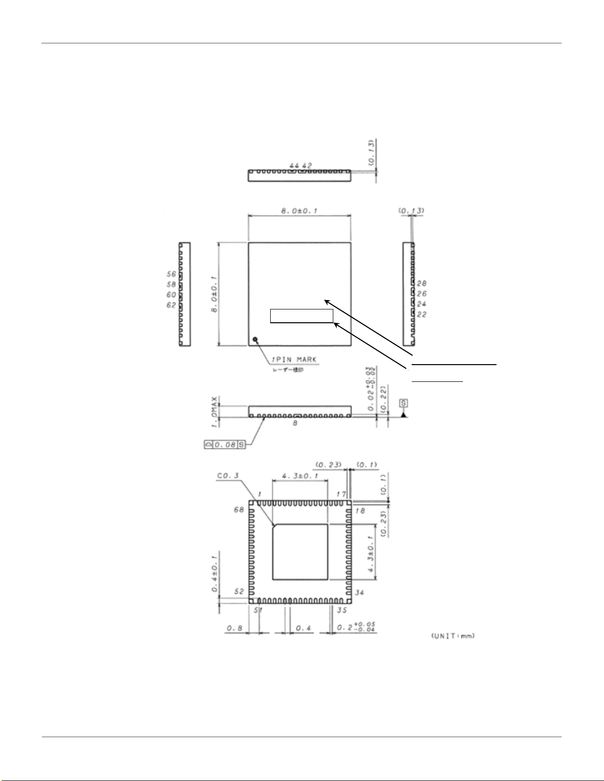
4.1. Package Dimension of BD71837MWV
Figure 4.1 The package dimension of BD71837MWV
7/46
Page 8

Application Note
BD71837MWV Platform Design Guide
© 2018 ROHM Co., Ltd.
No. 61AN002E Rev.001
May.2018
LDO4_FB
LDO4_VOUT
VSYS2
WDOG_B
RTC_RESET_B
BUCK8_FB
BUCK8_VIN
BUCK8_VIN
BUCK8_LX
BUCK8_LX
BUCK7_LX
BUCK7_VIN
BUCK7_FB
IRQ_B
POR_B
C32K_OUT
DVDD
(**)EXP-PAD
(**)EXP-PAD
LDO3_FB
VIN_3P3
LDO3_VOUT
VSYS3
BUCK4_FB
BUCK4_VIN
BUCK4_LX
BUCK3_LX
BUCK3_LX
BUCK3_VIN
BUCK3_FB
AGND
INTLDO1P5
LDO7_VOUT
VSYS1
XIN
XOUT
454443424140515049484746SDA33SCL32PMIC_ON_REQ
31
PMIC_STBY_REQ
3938373635
34
27
BUCK1_LX
26
BUCK1_LX
25
BUCK2_LX
30
BUCK1_FB
29
BUCK1_VIN
28
BUCK1_VIN
21
BUCK2_FB
20
PWRON_B
19
LDO1_VOUT
24
BUCK2_LX
23
BUCK2_VIN
22
BUCK2_VIN
18
LDO2_VOUT
12345678151617111213145591056
BUCK6_VIN
57
BUCK6_VIN
58
BUCK6_LX
68
LDO5_VOUT
(*)EXP-PAD
(PGND)
1Pin Mark
65
VIN_1P8_2
66
MUXSW_VOUT
BUCK6_FB
(**)EXP-PAD
(**)EXP-PAD
67
MUXSW_VOUT
62
BUCK5_VIN
63
BUCK5_VIN
64
BUCK5_FB
59
BUCK6_LX
60
BUCK5_LX
61
BUCK5_LX
52
VIN_1P8_1
53
LDO6_VOUT
54
SD_VSELECT
4.2. Pin Configuration
The pin configuration of BD71837MWV is designed and it will result in the effective routings between PMIC and SoC, memory device
and other components.
Note: (*) EXP-PAD is the power GND for PMIC so it should be soldered to GND plane.
(**) EXP-PAD assigned to 4 corners are also the same potentials with (*) EXP-PAD.
Figure 4.2 BD71837MWV pin configuration
8/46
Page 9
Application Note
BD71837MWV Platform Design Guide
© 2018 ROHM Co., Ltd.
No. 61AN002E Rev.001
May.2018
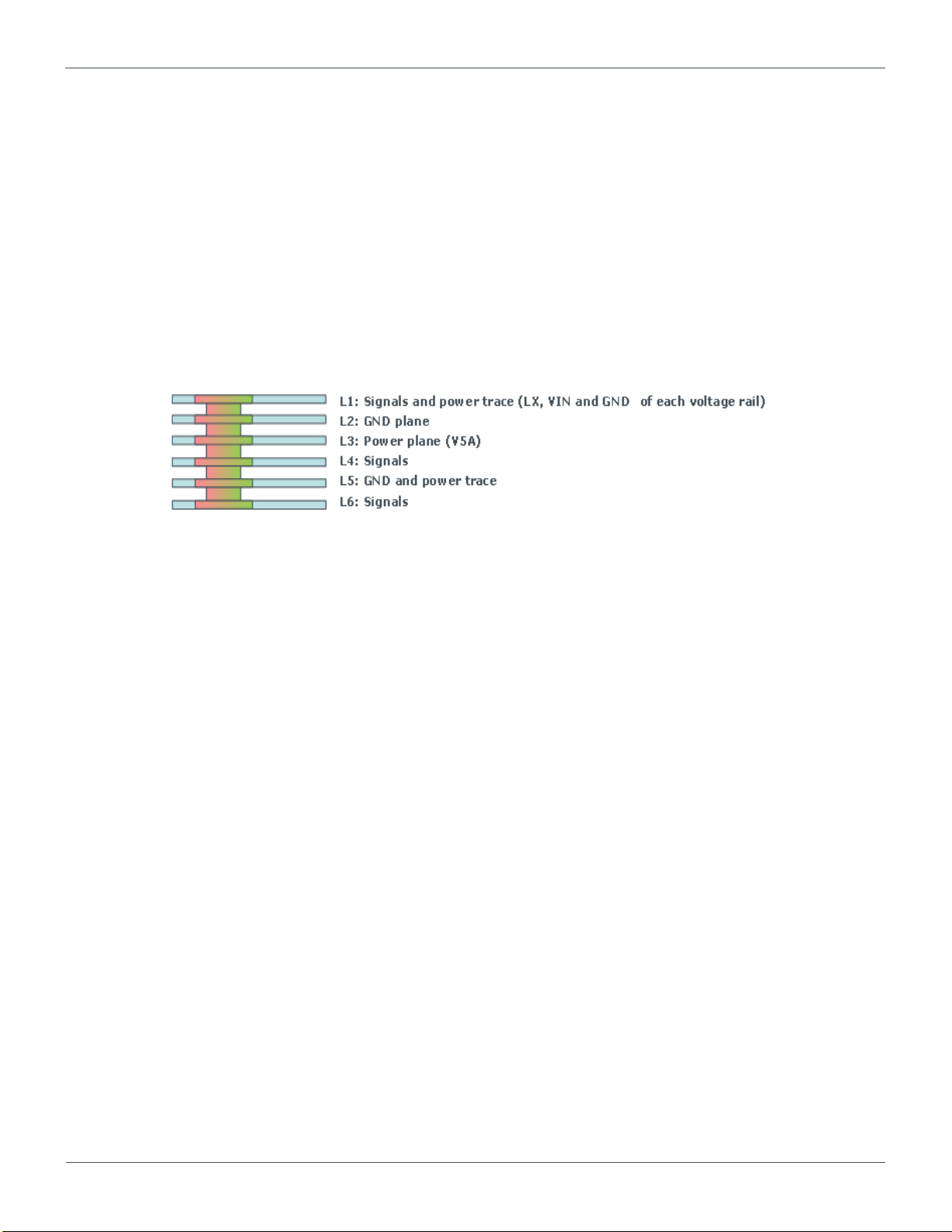
Figure 4.3 6-layers PCB stack-up
4.3. General Stack-up Recommendations
Type-3 and 6 layers PCB technology are used for BD71837MWV ROHM’s EVM.
The following general stack-up is strongly recommended to be applied to all the routings on the PCB.
Surface plane layers are recommended to apply 1.9 Mils thick copper.
Internal plane layers are recommended to apply 1.2 Mils thick copper.
It is recommended I2C signals to have the reference versus solid planes over the length of their routing and not to
cross plane splits. Ground should be the ideal reference.
The extra area in each layers should be filled with as much ground or other power rails as possible.
There should not be any large free areas with no metal for each layer because of the improvement for heat
dissipation. Large metal area also reduces stray resistance and inductance.
4.4. 6-layer Board Stack-up
BD71837MWV ROHM’s EVM uses Type 3 PCB technology and Figure 4.3 shows the 6-layer PCB stack-up.
9/46
Page 10
Application Note
BD71837MWV Platform Design Guide
© 2018 ROHM Co., Ltd.
No. 61AN002E Rev.001
May.2018
Via type
Hole size
Pad size
Anti-Pad size
Plated through-hole (PTH)
12 mils
24 mils
32 mils
Hole size
Pad size
Anti-Pad size
Figure 4.4 The image of PTH vias
4.5. Via Guidelines
This section explains proper via-drill, pad, and anti-pad size.
Note:
Improper drill, pad, and anti-pad size may cause some troubles on the PCB cost, reliability, manufacturability, and electrical
characteristics.
Type-3 PCB technology employs plated through-hole (PTH) vias for breakout routing. The dimension of PTH vias may vary as
necessary. Table 2.1 shows the recommended via dimension used for the breakout areas of BD71837MWV. Figure 4.4 shows the
image of PTH vias.
Table 4.1 Dimension example for PTH
10/46
Page 11
Application Note
BD71837MWV Platform Design Guide
© 2018 ROHM Co., Ltd.
No. 61AN002E Rev.001
May.2018
500μm or more
Current
flow
Exposed pad
Figure 4.5 The clearance between PTH and the exposed pad
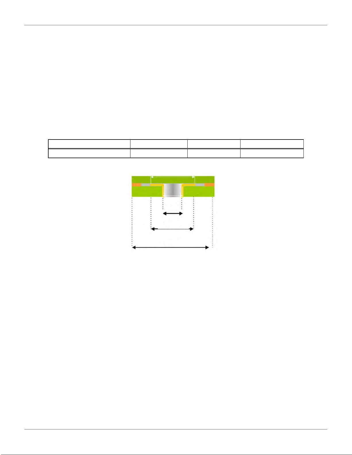
4.6. Placement of PTHs underneath the exposed pad
When the distance between the edge of metal mask of the exposed pad and PTH is close, the solder may get on the resist then the
PTH and exposed pad of BD71837MWV will be shorted. To avoid the soldering issue, it is highly recommended to keep the positons
of PTHs away from the edge of the exposed pad by 500μm or more, and PTHs should be placed not to disrupt the current flows
between each GND of the output capacitors and the exposed pad.
Note
The spaces for the current flows between GNDs of each output capacitor and exposed pad for PMIC PGND should be ensured. So it
is recommended that the numbers of PTHs disturbing the current flows should be secured.
11/46
Page 12
Application Note
BD71837MWV Platform Design Guide
© 2018 ROHM Co., Ltd.
No. 61AN002E Rev.001
May.2018
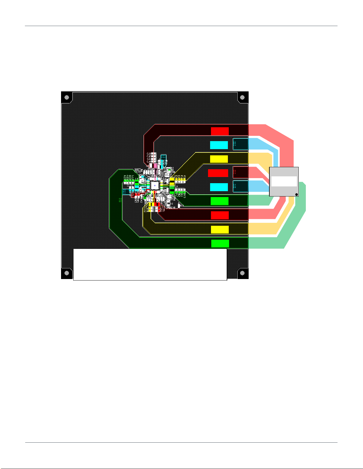
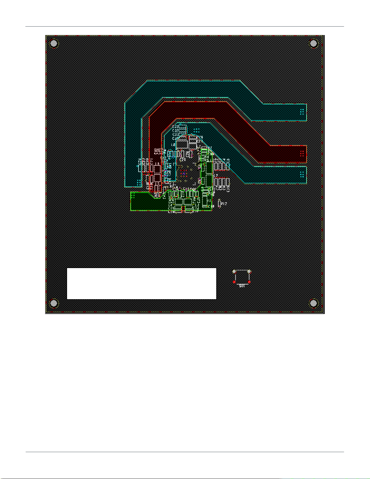
BUCK8
BUCK5
BUCK1
MUXSW
BUCK7
BUCK2
BUCK3
BUCK4
BUCK6
i.MX 8M
Top layer is used as power trace for each VR.
It’s better to secure the power traces with enough width to
relief the effect of the parasitic impedance.
Figure 4.6 BD71837MWV Reference Board Outline (Top Layer)
4.7. Outline for PCB layout
For understanding the outline of ROHM’s reference layout, the layout data for Layer 1(Top Layer) to 6 (Bottom layer) are shown in
Figure 4.6 to Figure 4.11.
The layout is designed, supposing the position of the SoC as Figure 4.6.
(1st pin of SoC is positioned at lower right.)
12/46
Page 13

Application Note
BD71837MWV Platform Design Guide
© 2018 ROHM Co., Ltd.
No. 61AN002E Rev.001
May.2018
GND
Layer 2 is used as power GND.
It’s better to secure the wide plane for large switching currents.
The parasitic impedance between PGND and each capacitor should be as low as possible.
Figure 4.7 BD71837MWV Reference Board Outline (Layer 2)
13/46
Page 14
Application Note
BD71837MWV Platform Design Guide
© 2018 ROHM Co., Ltd.
No. 61AN002E Rev.001
May.2018
VSYS
Layer 3 is used as VSYS power (Input for each VR).
It’s better to secure the wide plane for large input currents
which happens between input source and input capacitors.
Figure 4.8 BD71837MWV Reference Board Outline (Layer 3)
14/46
Page 15
Application Note
BD71837MWV Platform Design Guide
© 2018 ROHM Co., Ltd.
No. 61AN002E Rev.001
May.2018
Layer 4 is used as power traces for each VR.
It’s better to secure the enough width to relief the effect of
the parasitic impedance.
Figure 4.9 BD71837MWV Reference Board Outline (Layer 4)
15/46
Page 16

Application Note
BD71837MWV Platform Design Guide
© 2018 ROHM Co., Ltd.
No. 61AN002E Rev.001
May.2018
LDO4
LDO1
LDO2
LDO7
LDO3
LDO5
LDO6
Layer 5 is used as the power traces for each LDO.
It’s better to secure the enough width to relief the effect of
the parasitic impedance.
Figure 4.10 BD71837MWV Reference Board Outline (Layer 5)
16/46
Page 17

Application Note
BD71837MWV Platform Design Guide
© 2018 ROHM Co., Ltd.
No. 61AN002E Rev.001
May.2018
WDOG_B
SD_VSELECT
RTC_RESET_B
Layer 6 is used for routings of each feedback line and I/Os.
IRQ_B
POR_B
C32K_OUT
Figure 4.11 BD71837MWV Reference Board Outline (Layer 6)
17/46
Page 18

Application Note
BD71837MWV Platform Design Guide
© 2018 ROHM Co., Ltd.
No. 61AN002E Rev.001
May.2018
Voltage Rail
Type
Input Voltage
Default
Output Voltage
[V]
Max
Current
[mA]
Over Current
Protection
Min [mA]
BUCK1
Buck
VSYS
0.7 – 1.3
3600
5000
BUCK2
Buck
VSYS
0.7 – 1.3
4000
5500
BUCK3
Buck
VSYS
0.7 – 1.3
2100
3000
BUCK4
Buck
VSYS
0.7 – 1.3
1000
2500
BUCK5
Buck
VSYS
0.7 – 1.35
2500
3500
BUCK6
Buck
VSYS
3.0 – 3.3
3000
4500
BUCK7
Buck
VSYS
1.6 – 2.0
1500
3000
BUCK8
Buck
VSYS
0.8 – 1.4
3000
4500
LDO1
LDO
VSYS
1.6 – 1.9
10
20
LDO2
LDO
VSYS
0.9 / 0.8
10
20
LDO3
LDO
BUCK6 / VSYS
1.8 – 3.3
300
390
LDO4
LDO
BUCK7 / VSYS
0.9 – 1.8
250
325
LDO5
LDO
BUCK6
1.8 – 3.3
300
390
LDO6
LDO
BUCK7
0.9 – 1.8
300
340
LDO7
LDO
VSYS
1.8 – 3.3
150
195
MUXSW
Load Switch
1.8V / 3.3V
1.8 / 3.3
150
-
5. Platform Power Delivery Guidelines
BD71837MWV is the PMIC that incorporates single BUCK regulators, LDOs, and the internal load switch.
It is essential to follow the guidelines to ensure the stable power delivery to the SoC and the system.
5.1. Platform Power Delivery
Figure 5.1 shows the voltages BD71837MWV provides to the SoC and other devices in the system and the information of the
maximum currents for each VR are summarized in Table 5.1.
Table 5.1 The Maximum Design Powers for BUCK convertors, LDOs, and the Load Switch
18/46
Page 19

Application Note
BD71837MWV Platform Design Guide
© 2018 ROHM Co., Ltd.
No. 61AN002E Rev.001
May.2018
0.9V
0.9V/1.0V
0.9V/1.0V
0.9V/1.0V
1.0V
3.3V
0.9V
3.3V
3.3V
1.8V
1.8V
1.8V
0.9V
0.9V
VSYS(5V)
1.1/1.2/1.35V
PMIC_STBY_REQ
HOST
I/F
32kHz
Xtal
Driver
150mA MUXSW
BD71837MWV
1.8V/3.3V(SD CARD)1.8V
3.3V
I2C I/F
WDOG_B
PMIC_ON_REQ
POR_B
RTC_RESET_B
SD_VSELECT
IRQ_B
XOUT
XIN
C32K_OUT
BUCK6
3.0A, 3.0 to 3.3V
/0.1V step
BUCK7
1.5A, 1.6V to 2.0V
/ 8steps
NVCC_DRAM
VDD_SOC
VDD_ARM
VDD_GPU
VDD_VPU
VDD_DRAM
NVCC_SNVS
3P3_PHY
GPIO_3V3
VDD_SNVS
VDDA_1P8
1P8_PHY
GPIO_1V8
VDDA_0P9
0P9_PHY
iMX8M
VDDA_DRAM
BUCK1 – DVS
3.6A, 0.7V to 1.3V
/10mV step
BUCK2 – DVS
4.0A, 0.7V to 1.3V
/10mV step
BUCK3 – DVS
2.1A, 0.7V to 1.3V
/10mV step
BUCK4 – DVS
1.0A,0.7V to 1.3V
/10mV step
BUCK5
2.5A,0.7V to 1.35V
/ 8steps
BUCK8
3.0A,0.8V to 1.4V
/10mV step
LDO1
10mA,3.0V to 3.3V
/1.6V to 1.9V
LDO2
10mA,
0.9V/0.8V
LDO7
150mA,
1.8V to 3.3V
LDO3
300mA,
1.8V to 3.3V
LDO5
300mA,
1.8V to 3.3V
LDO4
250mA,
0.9V to 1.8V
LDO6
300mA,
0.9V to 1.8V
PWRON_B
Figure 5.1 BD71837MWV Power Delivery Map
19/46
Page 20

Application Note
BD71837MWV Platform Design Guide
© 2018 ROHM Co., Ltd.
No. 61AN002E Rev.001
May.2018
BUCK1
BUCK6
BCUK7
BUCK8
BUCK4
BUCK3
BUCK5
LDO4
LDO1
LDO5
MUXSW
LDO7
LDO3
LDO6
5.2. General Layout Guideline
This section explains the guideline about the layout for voltage regulators. The voltage rails with higher Iomax current especially for
BUCK convertors should be carefully designed not to transmit the unwanted interference caused by switching noises to other signals
with high impedance.
And IR drop caused by large switching currents often influence the violation of the stability for the input level for each buck convertor
so the design for each input should be also taken care. It is highly recommended to follow the all guidelines in this section.
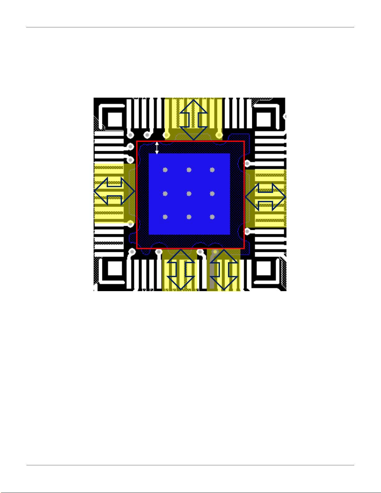
5.2.1. Overall Component Placement
Figure 5.2 shows the overall parts placement. The figure shows the positions of the components needed to be put closely to PMIC. It
is strongly recommended that the components controlling the higher currents like input / output capacitors and inductors are placed in
priority to any other components to guarantee the stabilities of each VR.
Figure 5.2 Overall component placement example
20/46
Page 21

Application Note
BD71837MWV Platform Design Guide
© 2018 ROHM Co., Ltd.
No. 61AN002E Rev.001
May.2018
Cin
L
VIN
Vout
①
②
Cout
①
Tr2
Tr1
LX
GND
Cin
Cout
BUCK2
point
capacitor
Via for GND
Figure 5.4 Example of parts placement and routings for BUCK2 at the top layer
Figure 5.3 BUCK Convertor Large Current Loops
5.2.2. Large Current Loop
There are 2 high-pulsing current flow loops in the BUCK convertor system.
Loop1
When Tr2 turns ON, the loop starts from the input capacitor, to VIN terminal, to LX terminal, to L (inductor), to output capacitors, and
then returns to the input capacitor through GND.
Loop2
When Tr1 turns ON, the loop starts from Tr1, to L (inductor), to output capacitors, and then returns to Tr1 through GND.
To reduce the noise and improve efficiency, please minimize the impedance of the each loop.
Figure 5.3 shows the current loops to be designed carefully.
As Figure 5.4 shows, the patterns which handle the heavy currents should be routed as much shortly and widely as possible to
suppress the effect of the parasitic impedance coming from PCB layout, especially the node with drastic shift in current or voltage
level such as VIN (input voltage) and power ground (GND). Two vias with the diameter of 300μm are used for input and GND for each
input capacitor to make the impedance lower.
Via for input
Feedback
21/46
Page 22

Application Note
BD71837MWV Platform Design Guide
© 2018 ROHM Co., Ltd.
No. 61AN002E Rev.001
May.2018
VSYS
BD71837MWV
PTH
VSYS
(Top layer)
(Inner layer)
Input Cap
Figure 5.5 Layout for BUCK X_VIN and VSYS
5.2.3. Power GND
Power ground for BUCK Converters (exposed pad) is the noisy ground because of the current loops indicated in the previous section.
Thus, the power ground should take an area as large as possible to keep the impedance low and reduce the swing of ground voltage
level.
5.2.4. VSYS (Power supply for BD71837MWV analog circuit)
BUCK X_VIN (X is 1, 2, 3… and 8) of each VR’s input should be connected to VSYS plane directly to minimize the parasitic and
common impedance effects.
The enough numbers of vias for input capacitors should be used and the decoupling capacitors should be placed as close to PMIC as
possible. The reference layout (BD71837MWV reference layout) can be referred to for your reference.
5.2.5. Other Signal Pattern Precautions
Make sure to leave adequate space between noisy lines of voltage rail and serial interface (I2C).
5.2.6. Feedback Sense Lines
Feedback sense lines (e.g., BUCK1_FB, BUCK2_FB etc.) should be routed to monitor the accurate output voltages for each voltage
rail. In order to avoid the effects of IR drop and switching noise, please make sure that the feedback sense lines are independently
routed from the point near output capacitors.
As the method for voltage sensing, “Local sensing” is recommended in all VRs.
In addition, these lines are interfered by noisy lines since these sense lines are high impedance nodes. Please don’t route these
sense lines by overlapping with or in parallel with noisy lines such as LX, SCL and SDA.
Drastic voltage shift in feedback lines result in unexpected voltage violations.
22/46
Page 23

Application Note
BD71837MWV Platform Design Guide
© 2018 ROHM Co., Ltd.
No. 61AN002E Rev.001
May.2018
Figure 5.6 Connection between Power GND and Analog GND
5.2.7. AGND layout
AGND is recommended not to be connected to PGND for PMIC (exposed pad) directly to avoid noise effect. It’s better to short AGND
to a GND at inner GND plane (stable GND) through PTH.
The reference layout as above can be referred to.
23/46
Page 24

Application Note
BD71837MWV Platform Design Guide
© 2018 ROHM Co., Ltd.
No. 61AN002E Rev.001
May.2018
Pin Names
Dir.
Notes (Unit of parts size : mm)
Check
Buck1 (VDD_SoC)
BUCK1_VIN[1:0]
I
Connect to the 5V power supply in the system.
As a decoupling capacitor, use one 10μF.
Select the input capacitor with the capacitance≧3.5μF including the DC bias effect
at VSYS=5.0V.
<The recommended part of capacitor is shown below.>
A.LMK107BBJ106MALT, size:1608, capacitance: 10μF, tolerance:10V
BUCK1_LX[1:0]
O
Connect to BUCK1 via the inductor.
Connect one 0.47μH ±20% inductors to BUCK1_LX0 and 1.
Select the inductor to be used according to board area and cost restrictions.
<The recommended part of inductor is shown below.>
A.HMLE32251E-R47MSR, size: 3225 , Rated DC Current : 7.2A
As output capacitors, use two 22μF capacitors.
Select the output capacitors within the capacitance range defined in the datasheet
of BD71837MWV.
<The recommended part of 22μF capacitor is shown below.>
A.GRM188R60J226MEA0D, size:1608, capacitance: 22μF, tolerance:6.3V
BUCK1_FB
I
Connect to the sense pin of BUCK1_FB to near output capacitors.
5.3. BUCK Convertors
In this section, application circuits for each voltage rail are explained.
For more detail information, the document of “BD71837MWV schematic check list” can be referred to.
5.3.1. BUCK1 (VDD_SoC)
BUCK1 is a high-efficiency buck converter which converts VSYS (2.7V to 5.5V) voltage to a regulated voltage.
This VR can dynamically change its output voltage setting using the I2C interface. BUCK1 output voltage range is from 0.7V to 1.3V
by 10mV step.
5.3.1.1. Schematic Example
5.3.1.2. Schematic checklist
Figure 5.7 BUCK1 Schematic Example
Table 5.2 BUCK1 schematic checklist
Note: Some dummy pads for output capacitors should be prepared like the reference schematic for the fine tuning in the actual board.
24/46
Page 25

Application Note
BD71837MWV Platform Design Guide
© 2018 ROHM Co., Ltd.
No. 61AN002E Rev.001
May.2018
Output Cap
BUCK1_VIN
BUCK1_LX
Input Cap
Feedback
point
Inductor
5.3.1.3. Parts placement for each decoupling capacitor
About the parts placement for each capacitor around BUCK1, the below reference layout can be referred to.
BUCK1_FB should be connected to near output capacitors.
Figure 5.8 BUCK1 Layout Example (Top Layer)
5.3.2. BUCK2 (VDD_ARM)
BUCK2 is a high-efficiency buck converter which converts VSYS (2.7V to 5.5V) voltage to a regulated voltage. This VR can
dynamically change its output voltage setting using the I2C interface. BUCK2 output voltage range is from 0.7V to 1.3V by 10mV
step.
5.3.2.1. Schematic Example
Figure 5.9 BUCK2 Schematic Example
25/46
Page 26

Application Note
BD71837MWV Platform Design Guide
© 2018 ROHM Co., Ltd.
No. 61AN002E Rev.001
May.2018
Pin Names
Dir.
Notes (Unit of parts size : mm)
Check
BUCK2 (VDD_ARM)
BUCK2_VIN[1:0]
I
Connect to the 5V power supply in the system.
As a decoupling capacitor, use one 10μF.
Select the input capacitor with the capacitance≧3.5μF including the DC bias effect
at VSYS=5.0V.
<The recommended part of capacitor is shown below.>
A.LMK107BBJ106MALT, size:1608, capacitance: 10μF, tolerance:10V
BUCK2_LX[1:0]
O
Connect to BUCK2 via the inductor.
Connect one 0.47μH ±20% inductors to BUCK2_LX0 and 1.
Select the inductor to be used according to board area and cost restrictions.
<The recommended part of inductor is shown below.>
A.HMLE32251E-R47MSR, size: 3225 , Rated DC Current : 7.2A
As output capacitors, use two 22μF capacitors.
Select the output capacitors within the capacitance range defined in the datasheet
of BD71837MWV.
<The recommended part of 22μF capacitor is shown below.>
A.GRM188R60J226MEA0D, size:1608, capacitance: 22μF, tolerance:6.3V
BUCK2_FB
I
Connect to the sense pin of BUCK2_FB to near output capacitors.
Output Cap
BUCK2_VIN
BUCK2_LX
Input Cap
Feedback
point
Inductor
5.3.2.2. Schematic checklist
Table 5.3 BUCK2 schematic checklist
Note: Some dummy pads for output capacitors should be prepared like the reference schematic for the fine tuning in the actual board.
5.3.2.3. Layout Example
About the parts placement for each capacitor around BUCK2, the below reference layout can be referred to.
BUCK2_FB should be connected to near output capacitors.
Figure 5.10 BUCK2 Layout Example (Top Layer)
26/46
Page 27

Application Note
BD71837MWV Platform Design Guide
© 2018 ROHM Co., Ltd.
No. 61AN002E Rev.001
May.2018
Pin Names
Dir.
Notes (Unit of parts size : mm)
Check
BUCK3 (VDD_GPU)
BUCK3_VIN
I
Connect to the 5V power supply in the system.
As a decoupling capacitor, use one 4.7μF.
Select the input capacitor with the capacitance≧1.88μF including the DC bias effect
at VSYS=5.0V.
<The recommended part of capacitor is shown below.>
A.LMK107BJ475MA, size:1608, capacitance: 4.7μF, tolerance:10V
BUCK3_LX[1:0]
O
Connect to BUCK3 via the inductor.
Connect one 0.47μH ±20% inductors to BUCK3_LX0 and 1.
Select the inductor to be used according to board area and cost restrictions.
<The recommended part of inductor is shown below.>
A.MAMK2520HR47M, size: 2520 , Rated DC Current : 5.8A
As output capacitors, use one 22μF capacitor.
Select the output capacitors within the capacitance range defined in the datasheet of
BD71837MWV.
<The recommended part of 22μF capacitor is shown below.>
A.GRM188R60J226MEA0D, size:1608, capacitance: 22μF, tolerance:6.3V
BUCK3_FB
I
Connect to the sense pin of BUCK3_FB to near output capacitors.
5.3.3. BUCK3 (VDD_GPU)
BUCK3 is a high-efficiency buck converter which converts VSYS (2.7V to 5.5V) voltage to a regulated voltage. This VR can
dynamically change its output voltage setting using the I2C interface. BUCK3 output voltage range is from 0.7V to 1.3V by 10mV
step.
5.3.3.1. Schematic Example
5.3.3.2. Schematic Checklist
Figure 5.11 BUCK3 Schematic Example
Table 5.4 BUCK3 schematic checklist
Note: Some dummy pads for output capacitors should be prepared like the reference schematic for the fine tuning in the actual board.
27/46
Page 28

Application Note
BD71837MWV Platform Design Guide
© 2018 ROHM Co., Ltd.
No. 61AN002E Rev.001
May.2018
Output Cap
BUCK3_VIN
BUCK3_LX
Input Cap
Feedback
point
Inductor
5.3.3.3. Layout Example
About the parts placement for each capacitor around BUCK3, the below reference layout can be referred to.
BUCK3_FB should be connected to near output capacitors.
Figure 5.12 BUCK3 Layout Example (Top Layer)
28/46
Page 29

Application Note
BD71837MWV Platform Design Guide
© 2018 ROHM Co., Ltd.
No. 61AN002E Rev.001
May.2018
Pin Names
Dir.
Notes (Unit of parts size : mm)
Check
BUCK4 (VDD_VPU)
BUCK4_VIN
I
Connect to the 5V power supply in the system.
As a decoupling capacitor, use one 4.7μF.
Select the input capacitor with the capacitance≧1.88μF including the DC bias
effect at VSYS=5.0V.
<The recommended part of capacitor is shown below.>
A.LMK107BJ475MA, size:1608, capacitance: 4.7μF, tolerance:10V
BUCK4_LX
O
Connect to BUCK3 via the inductor.
Connect one 0.47μH ±20% inductors to BUCK3_LX.
Select the inductor to be used according to board area and cost restrictions.
<The recommended part of inductor is shown below.>
A.MAMK2520HR47M, size: 2520 , Rated DC Current : 5.8A
As output capacitors, use one 22μF capacitor.
Select the output capacitors within the capacitance range defined in the datasheet
of BD71837MWV.
<The recommended part of 22μF capacitor is shown below.>
A.GRM188R60J226MEA0D, size:1608, capacitance: 22μF, tolerance:6.3V
BUCK4_FB
I
Connect to the sense pin of BUCK4_FB to near output capacitors.
5.3.4. BUCK4 (VDD_VPU)
BUCK4 is a high-efficiency buck converter which converts VSYS (2.7V to 5.5V) voltage to a regulated voltage. This VR can
dynamically change its output voltage setting using the I2C interface. BUCK4 output voltage range is from 0.7V to 1.3V by 10mV
step.
5.3.4.1. Schematic Example
5.3.4.2. Schematic Checklist
Figure 5.13 BUCK4 Schematic Example
Table 5.5 BUCK4 schematic checklist
Note: Some dummy pads for output capacitors should be prepared like the reference schematic for the fine tuning in the actual board.
29/46
Page 30

Application Note
BD71837MWV Platform Design Guide
© 2018 ROHM Co., Ltd.
No. 61AN002E Rev.001
May.2018
Output Cap
BUCK4_VIN
BUCK4_LX
Input Cap
Feedback
point
Inductor
5.3.4.3. Layout Example
About the parts placement for each capacitor around BUCK4, the below reference layout can be referred to.
BUCK4_FB should be connected to near output capacitors.
Figure 5.14 BUCK4 Layout Example (Top Layer)
5.3.5. BUCK5 (VDD_DRAM)
BUCK5 is a high-efficiency buck converter which converts VSYS (2.7V to 5.5V) voltage to a regulated voltage. BUCK5 output voltage
is programmable by the register and its range is from 0.7V to 1.35V.
5.3.5.1. Schematic Example
Figure 5.15 BUCK5 Schematic Example
30/46
Page 31

Application Note
BD71837MWV Platform Design Guide
© 2018 ROHM Co., Ltd.
No. 61AN002E Rev.001
May.2018
Pin Names
Dir.
Notes (Unit of parts size : inch)
Check
BUCK5 (VDD_DRAM)
BUCK5_VIN[1:0]
I
Connect to the 5V power supply in the system.
As a decoupling capacitor, use one 10μF.
Select the input capacitor with the capacitance≧3.5μF including the DC bias effect
at VSYS=5.0V.
<The recommended part of capacitor is shown below.>
A.LMK107BBJ106MALT, size:1608, capacitance: 10μF, tolerance:10V
BUCK5_LX[1:0]
O
Connect to BUCK5 via the inductor.
Connect one 0.47μH ±20% inductors to BUCK5_LX[1:0].
Select the inductor to be used according to board area and cost restrictions.
<The recommended part of inductor is shown below.>
A.MAMK2520HR47M, size: 2520 , Rated DC Current : 5.8A
BUCK5_FB
I
As output capacitors, use one 22μF capacitor.
Select the output capacitors within the capacitance range defined in the datasheet
of BD71837MWV.
<The recommended part of 22μF capacitor is shown below.>
A.GRM188R60J226MEA0D, size:1608, capacitance: 22μF, tolerance:6.3V
5.3.5.2. Schematic Checklist
Table 5.6 BUCK5 schematic checklist
Note: Some dummy pads for output capacitors should be prepared like the reference schematic for the fine tuning in the actual board.
31/46
Page 32

Application Note
BD71837MWV Platform Design Guide
© 2018 ROHM Co., Ltd.
No. 61AN002E Rev.001
May.2018
Output Cap
BUCK5_VIN
BUCK5_LX
Input Cap
Feedback
point
Inductor
5.3.5.3. Layout Example
About the parts placement for each capacitor around BUCK5, the below reference layout can be referred to.
BUCK5_FB should be connected to near output capacitors.
Figure 5.16 BUCK5 Layout Example (Top Layer)
5.3.6. BUCK6 (NVCC_3P3)
BUCK6 is a high-efficiency buck converter which converts VSYS (2.7V to 5.5V) voltage to a regulated voltage. BUCK6 output voltage
is programmable by the register and its range is from 3.0V to 3.3V by 100mV step.
5.3.6.1. Schematic Example
Figure 5.17 BUCK6 Schematic Example
32/46
Page 33

Application Note
BD71837MWV Platform Design Guide
© 2018 ROHM Co., Ltd.
No. 61AN002E Rev.001
May.2018
Pin Names
Dir.
Notes (Unit of parts size : inch)
Check
BUCK6 (NVCC_3P3)
BUCK6_VIN[1:0]
I
Connect to the 5V power supply in the system.
As a decoupling capacitor, use one 22μF.
Select the input capacitor with the capacitance≧7.7μF including the DC bias effect
at VSYS=5.0V.
<The recommended part of capacitor is shown below.>
A.LMK107BBJ226MA-T, size:1608, capacitance: 22μF, tolerance:10V
BUCK6_LX[1:0]
O
Connect to BUCK6 via the inductor.
Connect one 1.0μH ±20% inductors to BUCK6_LX[1:0].
Select the inductor to be used according to board area and cost restrictions.
<The recommended part of inductor is shown below.>
A.MAMK2520H1R0M, size: 2520 , Rated DC Current : 3.1A
BUCK6_FB
I
As output capacitors, use two 22μF capacitors.
Select the output capacitors within the capacitance range defined in the datasheet
of BD71837MWV.
<The recommended part of 22μF capacitor is shown below.>
A.GRM188R60J226MEA0D, size:1608, capacitance: 22μF, tolerance:6.3V
Output Cap
BUCK6_VIN
BUCK6_LX
Input Cap
Feedback
point
Inductor
5.3.6.2. Schematic Checklist
Table 5.7 BUCK6 schematic checklist
Note: Some dummy pads for output capacitors should be prepared like the reference schematic for the fine tuning in the actual board.
5.3.6.3. Layout Example
Figure 5.18 BUCK6 Layout Example (Top Layer)
33/46
Page 34

Application Note
BD71837MWV Platform Design Guide
© 2018 ROHM Co., Ltd.
No. 61AN002E Rev.001
May.2018
Pin Names
Dir.
Notes (Unit of parts size : inch)
Check
BUCK7 (NVCC_1V8)
BUCK7_VIN
I
Connect to the 5V power supply in the system.
As a decoupling capacitor, use one 4.7μF.
Select the input capacitor with the capacitance≧1.88μF including the DC bias
effect at VSYS=5.0V.
<The recommended part of capacitor is shown below.>
A.LMK107BJ475MA, size:1608, capacitance: 4.7μF, tolerance:10V
BUCK7_LX
O
Connect to BUCK7 via the inductor.
Connect one 0.47μH ±20% inductors to BUCK7_LX.
Select the inductor to be used according to board area and cost restrictions.
<The recommended part of inductor is shown below.>
A.MAMK2520HR47M, size: 2520 , Rated DC Current : 5.8A
BUCK7_FB
I
As output capacitors, use one 22μF capacitor.
Select the output capacitors within the capacitance range defined in the datasheet
of BD71837MWV.
<The recommended part of 22μF capacitor is shown below.>
A.GRM188R60J226MEA0D, size:1608, capacitance: 22μF, tolerance:6.3V
5.3.7. BUCK7 (NVCC_1V8)
VBUCK7 is a high-efficiency buck converter which converts VSYS (2.7V to 5.5V) voltage to a regulated voltage. BUCK7 output
voltage is programmable by the register and its range is from 1.6V to 2.0V by eight steps.
5.3.7.1. Schematic Example
Figure 5.19 BUCK7 Schematic Example
5.3.7.2. Schematic Checklist
Table 5.8 BUCK7 schematic checklist
Note: Some dummy pads for output capacitors should be prepared like the reference schematic for the fine tuning in the actual board.
34/46
Page 35

Application Note
BD71837MWV Platform Design Guide
© 2018 ROHM Co., Ltd.
No. 61AN002E Rev.001
May.2018
Output Cap
BUCK7_VIN
BUCK7_LX
Input Cap
Feedback
point
Inductor
5.3.7.3. Layout Example
About the parts placement for each capacitor around BUCK7, the below reference layout can be referred to.
BUCK7_FB should be connected to near output capacitors.
Figure 5.20 BUCK7 Layout Example (Top Layer)
35/46
Page 36

Application Note
BD71837MWV Platform Design Guide
© 2018 ROHM Co., Ltd.
No. 61AN002E Rev.001
May.2018
Pin Names
Dir.
Notes (Unit of parts size : inch)
Check
BUCK8 (NVCC_DRAM)
BUCK8_VIN[1:0]
I
Connect to the 5V power supply in the system.
As a decoupling capacitor, use one 10μF.
Select the input capacitor with the capacitance≧3.5μF including the DC bias effect
at VSYS=5.0V.
<The recommended part of capacitor is shown below.>
A.LMK107BBJ106MALT, size:1608, capacitance: 10μF, tolerance:10V
BUCK8_LX[1:0]
O
Connect to BUCK8 via the inductor.
Connect one 0.47μH ±20% inductors to BUCK8_LX0 and 1.
Select the inductor to be used according to board area and cost restrictions.
<The recommended part of inductor is shown below.>
A.HMLE32251E-R47MSR, size: 3225 , Rated DC Current : 7.2A
BUCK8_FB
I
As output capacitors, use two 22μF capacitors.
Select the output capacitors within the capacitance range defined in the datasheet
of BD71837MWV.
<The recommended part of 22μF capacitor is shown below.>
A.GRM188R60J226MEA0D, size:1608, capacitance: 22μF, tolerance:6.3V
5.3.8. BUCK8 (NVCC_DRAM)
BUCK8 is a high-efficiency buck converter which converts VSYS (2.7V to 5.5V) voltage to a regulated voltage. BUCK8 output voltage
is programmable by the register and its range is from 0.8V to 1.4V by 10mV step.
5.3.8.1. Schematic Example
Figure 5.21 BUCK8 Schematic Example
5.3.8.2. Schematic Checklist
Table 5.9 BUCK8 schematic checklist
Note: Some dummy pads for output capacitors should be prepared like the reference schematic for the fine tuning in the actual board.
36/46
Page 37

Application Note
BD71837MWV Platform Design Guide
© 2018 ROHM Co., Ltd.
No. 61AN002E Rev.001
May.2018
Output Cap
BUCK8_VIN
BUCK8_LX
Cap
Feedback
point
Inductor
5.3.8.3. Layout Example
About the parts placement for each capacitor around BUCK8, the below reference layout can be referred to.
BUCK8_FB should be connected to near output capacitors.
Input
Figure 5.22 BUCK8 Layout Example (Top Layer)
37/46
Page 38

Application Note
BD71837MWV Platform Design Guide
© 2018 ROHM Co., Ltd.
No. 61AN002E Rev.001
May.2018
5.4. LDOs
5.4.1. LDO1 (NVCC_SNVS)
VLDO1 converts VSYS (2.7V to 5.5V) voltage to a regulated voltage.
LDO1 output voltage is programmable by the register and its range is from 3.0V to 3.3V or 1.6V to 1.9V by 100mV step.
LDO1 should be used as the input for DVDD and pull up voltages for IRQ_B, RTC_RESET_B, WDOG_B and I2C interface.
5.4.2. LDO2 (VDD_SNVS)
VLDO2 converts VSYS (2.7V to 5.5V) voltage to a regulated voltage.
LDO2 output voltage is programmable and can be selected between 0.8V and 0.9V by the register.
5.4.3. LDO3 (VDDA_1P8/VDDA_DRAM)
VLDO3 converts VSYS (2.7V to 5.5V) voltage to a regulated voltage when BUCK6 is OFF.
After BUCK6 is ON, the input source will be changed from VSYS to BUCK6 automatically.
LDO3 output voltage is programmable and its voltage range is from 1.8V to 3.3V by 100mV step.
5.4.4. LDO4 (VDDA_0P9)
VLDO4 converts VSYS (2.7V to 5.5V) voltage to a regulated voltage when BUCK7 is OFF.
After BUCK7 is ON, the input source will be changed from VSYS to BUCK7 automatically.
LDO4 output voltage is programmable and its voltage range is from 0.9V to 1.8V by 100mV step.
5.4.5. LDO5 (1P8_PHY)
VLDO5 converts BUCK6 voltage to the regulated voltage.
LDO5 output voltage is programmable and its voltage range is from 1.8V to 3.3V by 100mV step.
5.4.6. LDO6 (0P9_PHY)
VLDO6 converts BUCK7 voltage to the regulated voltage.
LDO6 output voltage is programmable and its voltage range is from 0.9V to 1.8V by 100mV step.
5.4.7. LDO7 (3P3_PHY)
VLDO7 converts VSYS (2.7V to 5.5V) voltage to the regulated voltage.
LDO7 output voltage is programmable and its voltage range is from 0.9V to 1.8V by 100mV step.
38/46
Page 39

Application Note
BD71837MWV Platform Design Guide
© 2018 ROHM Co., Ltd.
No. 61AN002E Rev.001
May.2018
Pin Names
Dir.
Notes (Unit of parts size : mm)
Check
LDO1 (NVCC_SNVS) : Vout = 3.0V-3.3V / 1.6V-1.9V , Iomax=10mA
LDO1
O
As the output capacitor, use one 1μF capacitor.
Select the output capacitors within the capacitance range defined in the datasheet
of BD71837MWV.
<The recommended part of capacitor is shown below.>
A.JMK105BJ105MV-F, size:1005, capacitance: 1.0μF, tolerance:6.3V
LDO2 (VDD_SNVS) : Vout = 0.9V / 0.8V , Iomax=10mA
LDO2
O
As the output capacitor, use one 1μF capacitor.
Select the output capacitors within the capacitance range defined in the datasheet
of BD71837MWV.
<The recommended part of capacitor is shown below.>
A.JMK105BJ105MV-F, size:1005, capacitance: 1.0μF, tolerance:6.3V
LDO3 (VDDA_DRAM) : Vout = 1.8V - 3.3V, Iomax=300mA
LDO3
O
As the output capacitor, use one 2.2μF capacitor.
Select the output capacitors within the capacitance range defined in the datasheet
of BD71837MWV.
<The recommended part of capacitor is shown below.>
A.JMK105BJ225MV-F, size:1005, capacitance: 2.2μF, tolerance:6.3V
5.4.8. Schematic Examples
5.4.8.1. Schematic Checklist
Figure 5.23 LDO1 to 7 Schematic Example
Table 5.10 LDO1-7 schematic checklist
39/46
Page 40

Application Note
BD71837MWV Platform Design Guide
© 2018 ROHM Co., Ltd.
No. 61AN002E Rev.001
May.2018
Pin Names
Dir.
Notes (Unit of parts size : mm)
Check
LDO4 (VDDA_0P9) : Vout = 0.9V - 1.8V, Iomax=250mA
LDO4
O
As the output capacitor, use one 2.2μF capacitor.
Select the output capacitors within the capacitance range defined in the datasheet
of BD71837MWV.
<The recommended part of capacitor is shown below.>
A.JMK105BJ225MV-F, size:1005, capacitance: 2.2μF, tolerance:6.3V
LDO5 (1.8V PHY) : Vout = 1.8 - 3.3V, Iomax=300mA
LDO5
O
As the output capacitor, use one 2.2μF capacitor.
Select the output capacitors within the capacitance range defined in the datasheet
of BD71837MWV.
<The recommended part of capacitor is shown below.>
A.JMK105BJ225MV-F, size:1005, capacitance: 2.2μF, tolerance:6.3V
LDO6 (0.9V PHY) : Vout = 0.9V - 1.8V, Iomax=300mA
LDO6
O
As the output capacitor, use one 2.2μF capacitor.
Select the output capacitors within the capacitance range defined in the datasheet
of BD71837MWV.
<The recommended part of capacitor is shown below.>
A.JMK105BJ225MV-F, size:1005, capacitance: 2.2μF, tolerance:6.3V
LDO7 (3.3V PHY) : Vout = 1.8V - 3.3V, Iomax=150mA
LDO7
O
As the output capacitor, use one 2.2μF capacitor.
Select the output capacitors within the capacitance range defined in the datasheet
of BD71837MWV.
<The recommended part of capacitor is shown below.>
A.JMK105BJ225MV-F, size:1005, capacitance: 2.2μF, tolerance:6.3V
Inputs for LDOs
VSYS1
I
As the input capacitor, use one 2.2μF capacitor.
<The recommended part of capacitor is shown below.>
A.GRM155R61A225KE95, size:1005, capacitance: 2.2μF, tolerance:10V
VSYS2
I
As the input capacitor, use one 2.2μF capacitor.
<The recommended part of capacitor is shown below.>
A.GRM155R61A225KE95, size:1005, capacitance: 2.2μF, tolerance:10V
VSYS3
I
As the input capacitor, use one 2.2μF capacitor.
<The recommended part of capacitor is shown below.>
A.GRM155R61A225KE95, size:1005, capacitance: 2.2μF, tolerance:10V
VIN_1P8_1
I
The input for LDO4, 6 and connect to BUCK7.
As the input capacitor, use one 4.7μF capacitor.
<The recommended part of capacitor is shown below.>
A.JMK105BBJ475MV-F, size:1005, capacitance: 4.7μF, tolerance:6.3V
VIN_3P3
I
The input for LDO3, 5, MUXSW and connect to BUCK6.
As the input capacitor, use one 4.7μF capacitor.
<The recommended part of capacitor is shown below.>
A.JMK105BBJ475MV-F, size:1005, capacitance: 4.7μF, tolerance:6.3V
40/46
Page 41

Application Note
BD71837MWV Platform Design Guide
© 2018 ROHM Co., Ltd.
No. 61AN002E Rev.001
May.2018
Pin Names
Dir.
Notes (Unit of parts size : mm)
Check
MUXSW : Vout = 1.8V / 3.3V, Iomax=150mA
VIN_1P8_2
I
The input for MUXSW and connect to BUCK7.
As the input capacitor, use one 4.7μF capacitor.
<The recommended part of capacitor is shown below.>
A.JMK105BBJ475MV-F, size:1005, capacitance: 4.7μF, tolerance:6.3V
MUXSW_VOUT[1:0]
O
As the output capacitor, use one 22μF capacitor.
Select the output capacitors within the capacitance range defined in the datasheet
of BD71837MWV.
<The recommended part of 22μF capacitor is shown below.>
A.GRM188R60J226MEA0D, size:1608, capacitance: 22μF, tolerance:6.3V
5.5. Load SW
5.5.1. MUXSW (NVCC_SD2)
VMUXSW is the internal load switch for SD card power.
MUXSW output voltage supports 1.8V and 3.3V which are determined by the setting of SD_VSELECT.
5.5.1.1. Schematic Examples
Figure 5.24 MUXSW Schematic Example
5.5.1.2. Schematic Checklist
Table 5.11 MUXSW schematic checklist
Note: According to the setting of SD_VSELECT by SoC, the output of MUXSW is determined.
When SD_VSELECT = 0V, "3.3V mode" is selected and VIN_3P3 is used as the input.
When SD_VSELECT = DVDD, "1.8V mode" is selected and VIN_1P8_2 is used as the input.
41/46
Page 42

Application Note
BD71837MWV Platform Design Guide
© 2018 ROHM Co., Ltd.
No. 61AN002E Rev.001
May.2018
Pin Names
Dir.
Notes (Unit of parts size : mm)
Check
Crystal Oscillator Driver
XIN
I
As the load capacitor, use one 18pF capacitor.
<The recommended part of capacitor is shown below.>
A.UMK063CH180JT-F, size:0603, capacitance: 18pF, tolerance:50V
XOUT
O
As the load capacitor, use one 18pF capacitor.
<The recommended part of capacitor is shown below.>
A.UMK063CH180JT-F, size:0603, capacitance: 18pF, tolerance:50V
C32K_OUT
Connect to SoC
5.6. Crystal Oscillator Driver
5.6.1. XIN / XOUT / C32K_OUT
BD71837MWV has the crystal oscillator driver for 32.768 kHz for RTC in SoC internally.
The external load capacitors of C49 and C50 shown in the Figure 5.25 are set to 18pF and this value was determined after fine tuning
the specific parameters for the crystal of ST3215SB32768H5HPWAA (Load capacitance is 12.5pF) together with ROHM’s evaluation
board.
So it is ideal to confirm the valid capacitance value supported by the crystal supplier finely since the peripheral environment around
the crystal including the crystal part number itself should be different from the condition in ROHM’s evaluation.
5.6.1.1. Schematic Examples
Figure 5.25 Crystal Oscillator Driver Schematic Example
5.6.1.2. Schematic Checklist
Table 5.12 Schematic checklist of crystal oscillator driver
Note: As the crystal oscillator for RTC clock circuit, 32.768 kHz and 12.5pF (KYOCERA) is used together with BD71837MWV
evaluation board.
It is recommended to tune the load capacitance finely in the actual set to guarantee the stable oscillation.
<The recommended part of capacitor is shown below.>
A. ST3215SB32768H5HPWAA, size:3215, Load capacitance: 12.5pF
42/46
Page 43

Application Note
BD71837MWV Platform Design Guide
© 2018 ROHM Co., Ltd.
No. 61AN002E Rev.001
May.2018
Crystal
XOUT
XIN
Load Cap
Load Cap
5.6.1.3. Layout Example
Crystal oscillator driver circuit is extremely sensitive to external environment like parasitic capacitance due to the long wirings for XIN
and XOUT. So it is recommended to position the Crystal oscillator part near PMIC to shorten the length of the wirings.
Figure 5.26 XIN / XOUT Layout Example (Top Layer)
43/46
Page 44

Application Note
BD71837MWV Platform Design Guide
© 2018 ROHM Co., Ltd.
No. 61AN002E Rev.001
May.2018
Pin Names
Dir.
Signal
Voltage
Level
System
Pull-up/Pull-down
(RTT)
Termination
if it is not
used
Notes
Check
I2C
DVDD
I
- - -
The input power source for
C32K_OUT and I2C interface.
Capacitor for decoupling, use one
1.0μF ± 20%
(size : 1005, capacitance : 1.0μF,
tolerance : 6.3V)
SCL
I
DVDD
Pulled up to DVDD
with 1kohm
-
Connect to SoC (Note)
If pull up resistor is prepared within
SoC,
the additional pull up resistor is not
needed.
SDA
I/O
DVDD
Pulled up to DVDD
with 1kohm
-
Connect to SoC (Note)
If pull up resistor is prepared within
SoC,
the additional pull up resistor is not
needed.
5.7. Interfaces
I2C interface is selected for the communication between PMIC and SoC.
5.7.1. I2C
Table 5.13 Schematic checklist of I2C
Note: Recommended to use LDO1 (NVCC_SNVS) as power source for DVDD.
If DVDD is not used as the pull up voltage for SCL and SDA, it's recommended to use NVCC_I2C in SoC as the pull up voltage.
44/46
Page 45

Application Note
BD71837MWV Platform Design Guide
© 2018 ROHM Co., Ltd.
No. 61AN002E Rev.001
May.2018
Pin Names
Dir.
Expected
Signal
Voltage
Level
Expected System
Pull-up/Pull-down
(RTT)
Termination
if it is not
used
Notes
Check
System Control - Reset, Power, and Control Signals
PWRON_B
I
VSYS
Pulled up to VSYS
with 100kohm
Pulled up to
VSYS
with 100kohm
Connect to Power Button
POR_B
O
BUCK6
Refer to
Notes
Pulled up to
BUCK6
with 10kohm
NC
Connect to SoC (Note1)
If pull up resistor is prepared within SoC,
the additional pull up resistor is not
needed.
IRQ_B
O
DVDD
Refer to
Notes
Pulled up to DVDD
with 10kohm
NC
Connect to SoC (Note2)
If pull up resistor is prepared within SoC,
the additional pull up resistor is not
needed.
RTC_RESET_B
O
DVDD
Refer to
Notes
Pulled up to DVDD
with 10kohm
NC
Connect to SoC (Note3)
If pull up resistor is prepared within SoC,
the additional pull up resistor is not
needed.
PMIC_STBY_REQ
I
DVDD
Refer to
Notes
-
-
Connect to SoC (Note4)
PMIC_ON_REQ
I
DVDD
Refer to
Notes
-
-
Connect to SoC (Note4)
WDOG_B
I
DVDD
Refer to
Notes
Pulled up to DVDD
with 10kohm
Pulled up to
DVDD
with 10kohm
Connect to SoC (Note2)
If pull up resistor is prepared within SoC,
the additional pull up resistor is not
needed.
SD_VSELECT
I
DVDD
Refer to
Notes
-
GND
Connect to SoC (Note5)
5.7.2. System Control – Reset, Power, and Control Signals
Table 5.14 Schematic checklist of System Control – Reset, Power, and Control Signals
Note1: The source for pull up should be BUCK6 to avoid a leakage current. POR_B keeps L level until PMIC_ON_REQ is issued by
SoC and POR_B is de- asserted during the power sequence.
Note2: If the power source for NVCC_GPIO1 in SoC is different from the voltage of DVDD in PMIC, the pull up voltage is set to
NVCC_GPIO1.
Note3: If DVDD is different from the voltage of NVCC_SNVS in SoC, the pull up voltage is set to NVCC_SNVS.
Note4: This signal comes from SoC so the signal voltage level depends on the power source for NVCC_SNVS.
Note5: The voltage level depends on the power source for NVCC_GPIO1 which is the power source for GPIO in SoC.
45/46
Page 46

Application Note
BD71837MWV Platform Design Guide
© 2018 ROHM Co., Ltd.
No. 61AN002E Rev.001
May.2018
Pin Names
Dir.
Signal
Voltage Level
Notes
Check
MISC
AGND
-
GND
Connect to PGND at inner GND plane
EXP-PADs
(PGND0~4)
-
GND
Connect to the inner GND plane with lower impedance
5.7.3. MISC
Table 5.15 Schematic checklist of MISC
Note: The package has one pad at bottom and four corner pads to fix the position of the part.
These pads are shorted internally and it is recommended to solder these pads to the board.
46/46
Page 47

Notes
The information contained herein is subject to change without notice.
1)
Before you use our Products, please contact our sales representative
2)
tions :
Although ROHM is continuously working to improve product reliability and quality, semicon-
3)
ductors can break down and malfunction due to various factors.
Therefore, in order to prevent personal injury or fire arising from failure, please take safety
measures such as complying with the derating characteristics, implementing redundant and
fire prevention designs, and utilizing backups and fail-safe procedures. ROHM shall have no
responsibility for any damages arising out of the use of our Poducts beyond the rating specified by
ROHM.
Examples of application circuits, circuit constants and any other information contained herein are
4)
provided only to illustrate the standard usage and operations of the Products. The peripheral
conditions must be taken into account when designing circuits for mass production.
The technical information specified herein is intended only to show the typical functions of and
5)
examples of application circuits for the Products. ROHM does not grant you, explicitly or implicitly,
any license to use or exercise intellectual property or other rights held by ROHM or any other
parties. ROHM shall have no responsibility whatsoever for any dispute arising out of the use of
such technical information.
The Products specified in this document are not designed to be radiation tolerant.
6)
For use of our Products in applications requiring a high degree of reliability (as exemplified
7)
below), please contact and consult with a ROHM representative : transportation equipment (i.e.
cars, ships, trains), primary communication equipment, traffic lights, fire/crime prevention, safety
equipment, medical systems, servers, solar cells, and power transmission systems.
Do not use our Products in applications requiring extremely high reliability, such as aerospace
8)
equipment, nuclear power control systems, and submarine repeaters.
ROHM shall have no responsibility for any damages or injury arising from non-compliance with
9)
the recommended usage conditions and specifications contained herein.
ROHM has used reasonable care to ensurH the accuracy of the information contained in this
10)
document. However, ROHM does not warrants that such information is error-free, and ROHM
shall have no responsibility for any damages arising from any inaccuracy or misprint of such
information.
Please use the Products in accordance with any applicable environmental laws and regulations,
11)
such as the RoHS Directive. For more details, including RoHS compatibility, please contact a
ROHM sales office. ROHM shall have no responsibility for any damages or losses resulting
non-compliance with any applicable laws or regulations.
When providing our Products and technologies contained in this document to other countries,
12)
you must abide by the procedures and provisions stipulated in all applicable export laws and
regulations, including without limitation the US Export Administration Regulations and the Foreign
Exchange and Foreign Trade Act.
This document, in part or in whole, may not be reprinted or reproduced without prior consent of
13)
ROHM.
and verify the latest specifica-
Notice
ZZZURKPFRP
652+0&R/WG$OOULJKWVUHVHUYHG
Thank you for your accessing to ROHM product informations.
More detail product informations and catalogs are available, please contact us.
ROHM Customer Support System
http://www.rohm.com/contact/
5
%
 Loading...