


Power Management IC Series for Automotive Body Control
Motor Driver
BD6941FM
●Description
BD6941FM is the reversible motor driver for output 1.25A (1Motor), and can control a DC motor in four modes (Forward,
Reverse, Standby, Brake) corresponding to two control logic inputs.
●Features
1) 1ch DMOS H bridge output
2) Four output states ( Forward,Reverse,Standby,Brake ) by two control logic
3) Built-in surge-absorbing diodes
4) Low standby current
5) Output overcurrent protection with timer.
6) Over voltage detection switch off
7) TSD detects junction temperature and circuitry switches off the outputs at high temperature.
8) Built-in protection monitor pin (PO)
●Applications
Onboard devices(Vehicle equipment etc)
●Absolute Maximum Ratings(Ta= 25 ℃)
PARAMETER SYMBOL LIMIT UNIT
SUPPLY VOLTAGE Vcc 50 V
INPUT VOLTAGE V
OUTPUT CURRENT IO 1.25 (*1) A
POWER DISSIPATION Pd 2.8 (*2) W
OPERATING TEMPERATURE Topr -40~105 ℃
INP
, V
-0.3~20 V
INN
No.09039EAT02
STORAGE TEMPERATURE Tstg -55~150 ℃
JUNCTION TEMPERATURE Tjmax 150 ℃
*1 Not to exceed Pd and ASO.
*2 Mounted on a glass epoxy PCB (70mm×70mm×1.6mm).
To use at temperature above Ta=25℃ reduce 22.4mW/℃.
●Operating Range
PARAMETER SYMBOL LIMIT UNIT
SUPPLY VOLTAGE Vcc 8.0~16.0 V
www.rohm.com
© 2009 ROHM Co., Ltd. All rights reserved.
1/8
2009.06 - Rev.A

BD6941FM
●Electrical Characteristics(Unless otherwise specified, Vcc=8V~16V, Ta=-40℃~105℃)
PARAMETER SYMBOL
MIN. TYP. MAX
LIMIT
UNIT CONDITIONS
Circuit current 1 Icc1 - 0 10 μA Standby mode
Circuit current 2 Icc2 - 3 8 mA Forward or reverse mode
Circuit current 3 Icc3 - 3 8 mA Brake mode
Input Voltage “H” level VIH 3.0 - - V
Input Voltage “L” level VIL - - 1.0 V
“H” level input current IIH - 50 100 μA VIN=5.0V, flowing in current
“L” level input current IIL - 0 10 μA VIN=0V, flowing out current
Output on voltage 1 V
Output on voltage 2 V
Output leakage current “H” ILH - 0 10 μA V
Output leakage current “L” ILL - 0 10 μA V
Upper free-wheeling
diode forward voltage
Lower free-wheeling
diode forward voltage
Protection monitor voltage V
Protection monitor
leakage current
Over current protection switch
on current
Over Voltage Lockout
lockout switch on voltage
- 0.84 1.5 V Vcc=12V, I
ON1
- - 1.7 V
ON2
V
0.3 1.0 1.5 V IF=0.6A
FH
V
0.3 1.0 1.5 V IF=0.6A
FL
- - 0.6 V IPO=3mA
LPO
I
- 0 10 μA VPO=Vcc
LPO
I
1.5 - 3.5 A
OCP
V
25 30 35 V
OVP
out
Vcc=8~16V, I
total drop
=0V
OUT
=Vcc
OUT
=0.5A, total drop
out
Technical Note
=0.5A,
●Heat Reduction Curve
Pd(W)
3.0
2.8
2.0
1.0
50 75 100 125 150 Ta(℃)0
105
Mounted on a glass epoxy PCB (70mm×70mm×1.6mm)
To use at temperature above Ta=25℃ reduce 22.4mW/℃.
www.rohm.com
© 2009 ROHM Co., Ltd. All rights reserved.
2/8
2009.06 - Rev.A
BD6941FM
Technical Note
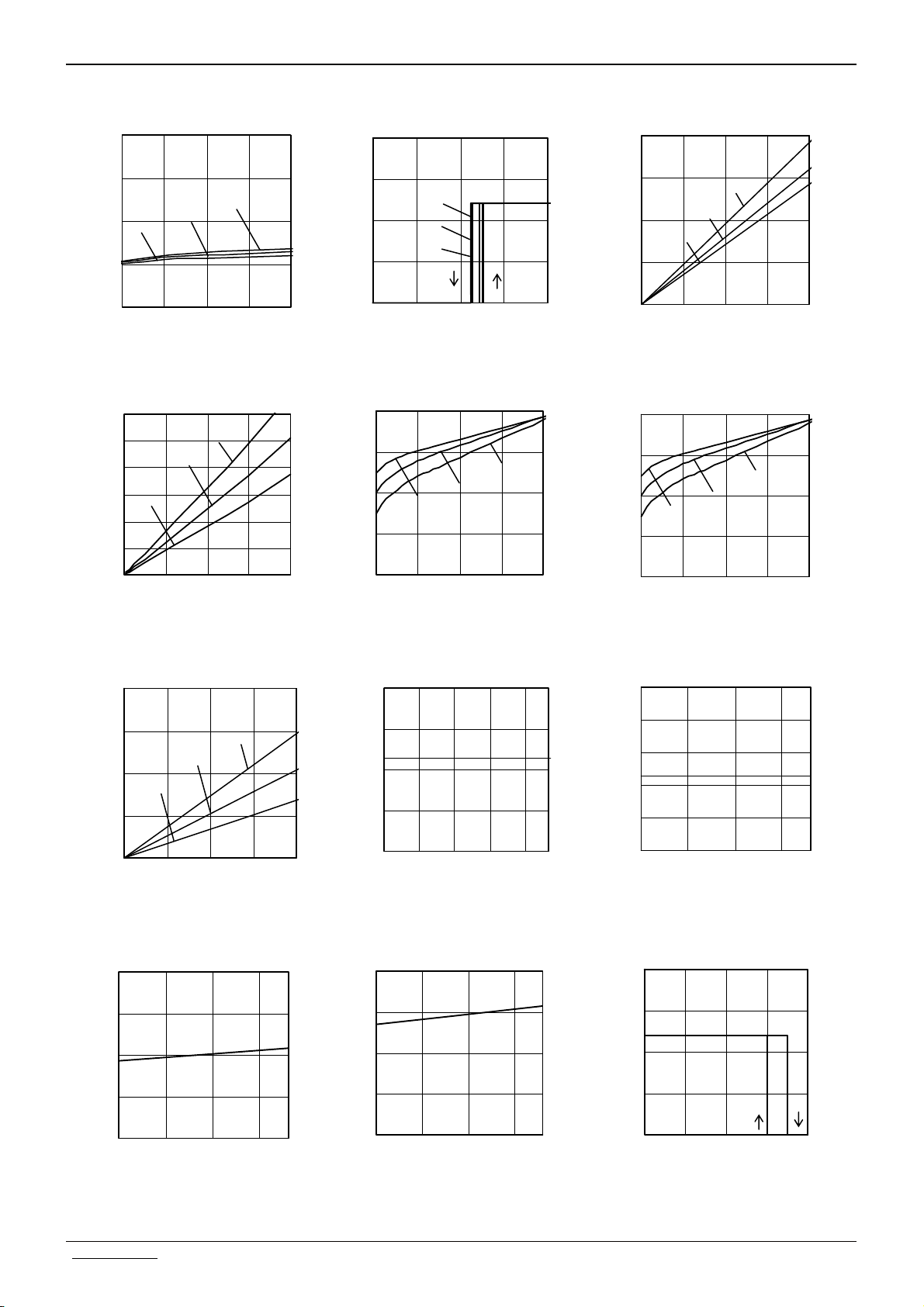
●Reference Data
8
20
200
6
Ta= 1 05
A]
m
4
Icc[
Ta=
2
Ta= 2 5℃
-40℃
℃
[V]
OUT
V
15
Ta= 1 05
℃
10
Ta= 2 5℃
Ta= -40℃
5
150
A]
μ
100
[
IN
I
Ta= -40℃
50
Ta= 2 5
Ta= 1 05
℃
0
810121416
Vcc[V]
0
01234
VIN[V]
0
0 4 8 12 16
VIN[V]
Fig.1 Circuit current Fig.2 Input voltage vs. Output voltage Fig.3 Input H current
(Forward・Reverse・Brake)
3
2.5
2
]
V
[
1.5
Ta= -40℃
ON
V
1
0.5
0
0 0.4 0.8 1.2 1.6
Ta= 2 5℃
Ta= 1 05 ℃
[A]
I
OUT
1.2
0.9
]
V
[
0.6
FH
V
0.3
0.0
Ta= -40℃
0.0 0.4 0.8 1.2 1.6
Ta= 2 5℃
[A]
I
OUT
Ta= 1 05 ℃
1.2
0.9
Ta= 2 5℃
I
OUT
Ta= 1 05 ℃
[A]
]
V
[
0.6
FL
V
Ta= -40℃
0.3
0.0
0.0 0.4 0.8 1.2 1.6
Fig.4 Output on voltage(Vcc=12V) Fig.5 Upper free-wheeling Fig.6 Upper free-wheeling
diode forward voltage H diode forward voltage L
0.16
4
0.12
[V]
0.08
PO
Ta= -40℃
V
0.04
Ta= 1 05 ℃
Ta= 2 5℃
3
2
Iocp[A]
1
[V]
OV
V
35
33
31
29
27
℃
0
01234
IPO[mA]
0
-40 -10 20 50 80
Ta[℃]
25
-40 0 40 80
Ta[℃]
Fig.7 Protection monitor voltage Fig.8 Over current protection Fig.9 Over Voltage Lockout
switch on current lockout switch on voltage
20
400
20
15
10
[μs]
ON
T
5
0
-40 0 40 80
Fig.10 Over current protection Fig.11 Over current protection Fig.12 TSD temperature
Ta[℃]
300
[μs]
200
OFF
T
100
0
-40 0 40 80
Ta[℃]
15
[V]
10
OUT
V
5
0
0 50 100 150 200
Ta[℃]
monitor on time monitor off time
www.rohm.com
© 2009 ROHM Co., Ltd. All rights reserved.
3/8
2009.06 - Rev.A

BD6941FM
Technical Note
●Block Diagram ●Terminal Function Table
N.C.
N.C.
N.C.
N.C.
N.C.
N.C.
SGND
MN
MN
Vcc
Vcc
N.C.
N.C.
N.C.
N.C.
N.C.
SGND
PO
1
2
3
4
5
6
7
8
9
10
11
TSD
12
13
14
15
PROTECTION
MONITOR
16
17
18
OVER
VO LTAG E
PROTECTION
PROTECT ION
CONTROL
LOGIC
M
OVER
CURRENT
PIN No. Terminal Name Function
N.C.
36
N.C.
35
N.C.
34
N.C.
33
N.C.
32
PGND
31
PGND
30
MP
29
28
MP
N.C.
27
N.C.
.
26
N.C.
25
N.C.
24
N.C.
23
N.C.
22
SGND
21
INN
20
INP
19
1-6 N.C. N.C.
7 SGND Signal GND Pin
8 MN Motor Output Pin
9 MN Motor Output Pin
FIN FIN FIN
10 Vcc Power Supply Pin
11 Vcc Power Supply Pin
12-16 N.C. N.C.
17 SGND Signal GND Pin
18 PO
Protection Monitor
Pin(Open drain)
19 INP Logic Input Pin
20 INN Logic Input Pin
21 SGND Signal GND Pin
22-27 N.C. N.C.
FIN FIN FIN
28 MP
29 MP
Motor Output Pin
Motor Output Pin
30 PGND Power GND Pin
31 PGND Power GND Pin
32-36 N.C. N.C.
●Package
BD6941FM
1 PIN mark
Lot No.
HSOP-M36(Unit : mm)
www.rohm.com
© 2009 ROHM Co., Ltd. All rights reserved.
4/8
2009.06 - Rev.A

BD6941FM
A
●Signal Table
Input/Output Truth Table
Technical Note
Output Condition
IN OUT
MODE
INP INN MP MN
H H L L BRAKE
H L H L FORWARD
L H L H REVERSE
L L Open Open STANDBY
IN OUT
PO
INP INN MODE LOAD
NORMAL H
H H BRAKE
SHORT L *2
FORWARD/
NORMAL H
H/L L/H
REVERSE
SHORT L *2
L L STANDBY - H
*2 refer to timing chart
●PO Output Timing Chart
OCP
I
Output current
0
MP/MN
PO
normal over current detection
T
OFF
T
ON
normal
T
≒ 10μsec
ON
T
≒ 290μsec
OFF
ctive
Open
www.rohm.com
© 2009 ROHM Co., Ltd. All rights reserved.
5/8
2009.06 - Rev.A

BD6941FM
●I/O Circuit Diagram
1) INP, INN 2) PO
Technical Note
INP
INN
3) MP, MN
Vcc
100K
SGND
Vcc
MP, MN
Vcc
PO
SGND
PGND
Operating Notes
●
1) Absolute maximum ratings
Use of the IC in excess of absolute maximum ratings such as the applied voltage or operating temperature range may result
in IC damage. Assumptions should not be made regarding the state of the IC (short mode or open mode) when such damage
is suffered. A physical safety measuresuch as a fuse should be implemented when use of the IC in a special mode where the
absolute maximum ratings may be exceeded is anticipated.
2) GND potential
Ensure a minimum GND pin potential in all operating conditions.
3) Thermal design
Use a thermal design that allows for a sufficient margin in light of the power dissipation (Pd) in actual operating conditions.
4) Pin short and mistake mounting
Use caution when orienting and positioning the IC for mounting on printed circuit boards. Improper mounting may result in
damage to the IC.Shorts between output pins and the power supply and GND pins caused by the presence of a foreign
object may result in damage to the IC. Ensure a minimum GND pin potential in all operating conditions.
5) Actions in strong magnetic field
Keep in mind that the IC may malfunction in strong magnetic fields.
6) Testing on application boards
When testing the IC on an application board, connecting a capacitor to a pin with low impedance subjects the IC to stress.
Always discharge capacitors after each process or step. Always turn the IC's power supply off before connecting it to or
removing it from a jig or fixture during the inspection process. Ground the IC during assembly steps as an antistatic measure,
and use similar caution when transporting or storing the IC.
www.rohm.com
© 2009 ROHM Co., Ltd. All rights reserved.
6/8
2009.06 - Rev.A

BD6941FM
Technical Note
7) IC terminal input voltage
This monolithic IC contains P+ isolation and P substrate layers between adjacent elements in order to keep them isolated.
P/N junctions are formed at the intersection of these P layers with the N layers of other elements to create a variety of
parasitic elements. For example, when the resistors and transistors are connected to the pins as shown in the following
figure,
The P/N junction functions as a parasitic diode when GND > Pin A for the resistor or GND > Pin B for the transistor(NPN).
Similarly, when GND > Pin B for the transistor (NPN), the parasitic diode described above combines with the N layer of
other adjacent elements to operate as a parasitic NPN transistor.
The formation of parasitic elements as a result of the relationships of the potentials of different pins is an inevitable result of
the IC's architecture. The operation of parasitic elements can cause interference with circuit operation as well as IC
malfunction and damage. For these reasons, it is necessary to use caution so that the IC is not used in a way that will trigger
the operation of parasitic elements, such as by the application of voltages lower than the GND (P substrate) voltage to input
pins.
(Pin A)
N
P
P+
Resistor
N
P
GND
P+
N
Parasitic elements
(Pin B)
C
P+
N
N
Parasitic elements
or Transistors
B
E
N
P
N
P substrate
GND
(Pin B)
(Pin A)
C
B
GND
Parasitic elements or
Parasitic elements
8) Input terminals
Do not apply the voltage to input pin when the Vcc is not applied. And when the Vcc is applied, the voltage of input pin
must not exceed Vcc. It is feared that output get malfunction, as input voltage is sweeped slowly near the H, L threshold
voltage. Please pay attention to input slew rate.
9) Back electro motive force (BEMF)
There is a possibility that the BEMF is changed by use of the operating condition, environment and the individual
characteristics of motor. Please make sure there is no problem of operating the IC although the BEMF is occurred.
10) The note of pattern design at printed circuit
This IC flows large current between power supply for motor division and GND. So, it is feared that get undesirable result
malfunction, oscillation and so on, as input lines is affected by large output current. Please consider pattern design at
printed circuit doesn’t have common impedance on output large current lines-input lines. Please consider to keep low
impedance of power supply for fear of oscillation from power supply high impedance, also.
11) Rash current
This IC doesn’t have current limit circuit for rash current. Therefore physical security countermeasure, like current limit
resistor is to be given.
12) Thermal shutdown circuit
This IC incorporates a built-in TSD circuit for the protection from thermal destruction. The IC should be used within the
specified power dissipation range. However, in the event that the IC continues to be operated in excess of its power
dissipation limits , the attendant rise in the junction temperature (Tj) will trigger the TSD circuit to turn off all output power
elements. The circuit automatically resets once the junction temperature (Tj) drops. Operation of the TSD circuit presumes
that the IC's absolute maximum ratings have been exceeded. Application designs should never make use of the TSD circuit.
13) Over voltage lock out function
This IC has the function of turning off the output when detecting the over voltage. More than 30V(typ.) triggers this
function. But in the standby mode, this function does not work. Although this IC has over voltage lockout function, the
voltage that exceeds absolute maximum ratings might destroy the IC. Please do not exceed the absolute maximum
ratings.
www.rohm.com
© 2009 ROHM Co., Ltd. All rights reserved.
7/8
2009.06 - Rev.A

BD6941FM
Technical Note
14)Over current protection
This IC has the function of turning off the output when detecting the over current. More than 2.25A(typ.) triggers this
function. When detecting the over current for 10μsec(typ.), this function turns off the output(output terminals become
Hi-impedance) for 290μsec(typ.). After the period of turning off time (290μsec) , the output current recovers. But if the
over current is still detected, this function will work again.This function is for protecting IC because of the output short etc.
but the continuing detection of over current might cause the extreme heat and damage the IC. It is recommended to
change the IC’s state to standby mode by the application. And please pay attention to the power dissipation.
●Ordering part number
B D 6 9 4 1 F M - E 2
Part No. Part No.
HSOP-M36
18.5± 0.1
(MAX 18.75 include BURR)
2.77±0.1
27
28
+6
4
–4
1936
9.9± 0.2
7.5± 0.1
0.85
1
9
1PIN MARK
18
10
0.27
+0.055
–0.045
0.5± 0.15
1.2± 0.2
Package
FM : HSOP-M36
<Tape and Reel information>
Embossed carrier tape (with dry pack)Tape
Quantity
Direction
of feed
1500pcs
E2
The direction is the 1pin of product is at the upper left when you hold
()
reel on the left hand and you pull out the tape on the right hand
Packaging and forming specification
E2: Embossed tape and reel
2.4MAX
2.2± 0.05
0.1± 0.05
0.8
–0.04
0.08
+0.05
0.37
0.08 S
M
(Unit : mm)
Reel
1pin
Order quantity needs to be multiple of the minimum quantity.
∗
Direction of feed
www.rohm.com
© 2009 ROHM Co., Ltd. All rights reserved.
8/8
2009.06 - Rev.A

Notes
No copying or reproduction of this document, in part or in whole, is permitted without the
consent of ROHM Co.,Ltd.
The content specied herein is subject to change for improvement without notice.
The content specied herein is for the purpose of introducing ROHM's products (hereinafter
"Products"). If you wish to use any such Product, please be sure to refer to the specications,
which can be obtained from ROHM upon request.
Examples of application circuits, circuit constants and any other information contained herein
illustrate the standard usage and operations of the Products. The peripheral conditions must
be taken into account when designing circuits for mass production.
Great care was taken in ensuring the accuracy of the information specied in this document.
However, should you incur any damage arising from any inaccuracy or misprint of such
information, ROHM shall bear no responsibility for such damage.
The technical information specied herein is intended only to show the typical functions of and
examples of application circuits for the Products. ROHM does not grant you, explicitly or
implicitly, any license to use or exercise intellectual property or other rights held by ROHM and
other par ties. ROHM shall bear no responsibility whatsoever for any dispute arising from the
use of such technical information.
Notice
The Products specied in this document are intended to be used with general-use electronic
equipment or devices (such as audio visual equipment, ofce-automation equipment, communication devices, electronic appliances and amusement devices).
The Products specied in this document are not designed to be radiation tolerant.
While ROHM always makes efforts to enhance the quality and reliability of its Products, a
Product may fail or malfunction for a variety of reasons.
Please be sure to implement in your equipment using the Products safety measures to guard
against the possibility of physical injury, re or any other damage caused in the event of the
failure of any Product, such as derating, redundancy, re control and fail-safe designs. ROHM
shall bear no responsibility whatsoever for your use of any Product outside of the prescribed
scope or not in accordance with the instruction manual.
The Products are not designed or manufactured to be used with any equipment, device or
system which requires an extremely high level of reliability the failure or malfunction of which
may result in a direct threat to human life or create a risk of human injury (such as a medical
instrument, transpor tation equipment, aerospace machinery, nuclear-reactor controlle r,
fuel-controller or other safety device). ROHM shall bear no responsibility in any way for use of
any of the Products for the above special purposes. If a Product is intended to be used for any
such special purpose, please contact a ROHM sales representative before purchasing.
If you intend to export or ship overseas any Product or technology specied herein that may
be controlled under the Foreign Exchange and the Foreign Trade Law, you will be required to
obtain a license or permit under the Law.
www.rohm.com
© 2009 ROHM Co., Ltd. All rights reserved.
Thank you for your accessing to ROHM product informations.
More detail product informations and catalogs are available, please contact us.
ROHM Customer Support System
http://www.rohm.com/contact/
R0039
A
 Loading...